

Page 1
General Description
The MAX9500/MAX9501 are fully integrated solutions
for filtering and buffering HDTV signals. The MAX9500
operates from a single +5V supply, while the MAX9501
operates from dual ±5V supplies. The MAX9500/
MAX9501 triple-channel video reconstruction filters are
both gain and delay matched and are ideal for use in
set-top boxes, DVD players, and other equipment that
generate analog HDTV outputs.
The MAX9500/MAX9501 interface between the currentoutput, digital-to-analog converters (DAC) of an
Advanced Television Standard Committee (ATSC),
Motion Picture Experts Group (MPEG) decoder and the
external connections of a television, set-top box, or
DVD player.
The MAX9500/MAX9501 feature a DC-coupled input with
very low input capacitance and high resistance. The
highly selective lowpass filters remove spectral replicas
at the output of the DAC. The output amplifier has +6dB
of gain to drive 75Ω back-terminated loads to unity gain.
The DC-coupled input eliminates problems such as sync
crush, droop, and field tilt. The output load can be DC- or
AC-coupled, depending on the application.
All three channels in the MAX9500/MAX9501 have the
same frequency response with matched group delay
and gain. The MAX9500/MAX9501 filter response meets
the requirements of the EIA-770.3/SMPTE274M filter
template achieving > 40dB attenuation at 44.25MHz.
The MAX9500/MAX9501 can also be used as an antialiasing filter for HDTV component inputs.
The MAX9500/MAX9501 are available in 16-pin SO and
compact 16-pin QSOP packages, and are fully specified
over the –40°C to +85°C extended temperature range.
Applications
Cable and Satellite Set-Top Box Receivers
A/V Receivers
Home Theater Systems
HDTV Sets
DVD Players
Video Projectors
Digital Displays
Features
♦ 30MHz Bandwidth at ±1.5dB
♦ Extremely Sharp Rolloff, Lowpass Filters
-50dB at 44.25MHz
♦ DC-Coupled Inputs; AC- or DC-Coupled Outputs
♦ ±5V Dual Supply (MAX9501)
♦ 5V Single Supply (MAX9500)
♦ Matched Group Delay and Gain
♦ Drive Single/Double Back-Terminated Loads
(150Ω/75Ω) Directly to Ground
♦ Sink and Source Output Current
♦ High Input Impedance to Interface to Low Output-
Current DAC
♦ 16-Pin SO and QSOP Packages
MAX9500/MAX9501
Triple-Channel HDTV Filters
________________________________________________________________ Maxim Integrated Products 1
Ordering Information
19-3779; Rev 1; 11/05
For pricing, delivery, and ordering information, please contact Maxim/Dallas Direct! at
1-888-629-4642, or visit Maxim’s website at www.maxim-ic.com.
PART
TEMP RANGE
PIN-
SUPPLY
VOLTAGE
(V)
MAX9500ESE+*
16 SO +5
MAX9500EEE+
16 QSOP +5
MAX9501ESE+*
16 SO ±5
MAX9501EEE+*
16 QSOP ±5
Pin Configurations appear at end of data sheet.
+Denotes lead-free package.
*Future product—contact factory for availability.
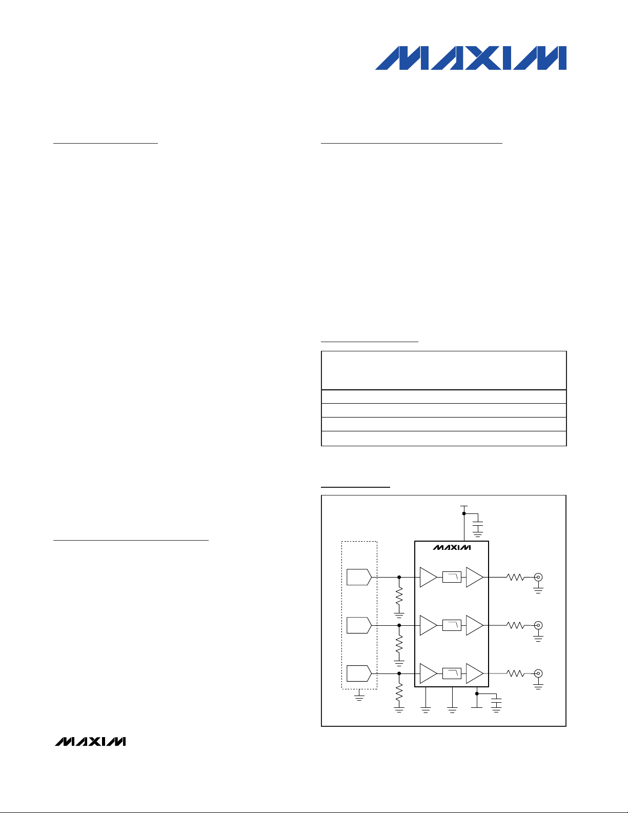
MAX9500
MAX9501
10-BIT
DAC
150Ω
75Ω
LPF
10-BIT
DAC
150Ω
75Ω
LPF
10-BIT
DAC
150Ω
75Ω
LPF
MPEG
DECODER
+6dB
+6dB
+6dB
YOUT
PbOUT
PrOUT
YIN
PbIN
PrIN
GND SUBG
(MAX9500)
0.1µF
V
CC
0.1µF
V
EE
(MAX9501)
Typical Operating Circuit
PACKAGE
-40°C to +85°C
-40°C to +85°C
-40°C to +85°C
-40°C to +85°C
Page 2
MAX9500/9501/MAX9501
Triple-Channel HDTV Filters
2 _______________________________________________________________________________________
ABSOLUTE MAXIMUM RATINGS
ELECTRICAL CHARACTERISTICS—MAX9500 (Single Supply)
(VCC= 5V, RL= ∞, TA= T
MIN
to T
MAX
, unless otherwise noted. Typical values are at TA= +25°C.) (Note 1)
Stresses beyond those listed under “Absolute Maximum Ratings” may cause permanent damage to the device. These are stress ratings only, and functional
operation of the device at these or any other conditions beyond those indicated in the operational sections of the specifications is not implied. Exposure to
absolute maximum rating conditions for extended periods may affect device reliability.
Positive Supply Voltage (VCCto GND) ....................-0.3V to +6V
Negative Supply Voltage (MAX9501)
(V
EE
to GND) ........................................................+0.3V to -6V
All Input Pins...............................................-0.3V to (V
CC
+ 0.3V)
All Output Pins (MAX9500).........................-0.3V to (V
CC
+ 0.3V)
All Output Pins (MAX9501) ............................(V
EE
- 0.3V) to +3V
Output Short-Circuit Duration
(OUT to V
CC
or GND) (MAX9500) ......................................10s
Output Short-Circuit Duration
(OUT to GND or V
EE
) (MAX9501)........................................10s
Continuous Input Current (YIN, PbIN, PrIN) .....................±20mA
Continuous Power Dissipation (T
A
= +70°C)
16-Pin SO (derate 13mW/°C above +70°C)...............1039mW
16-Pin QSOP (derate 12.8mW/°C above +70°C).......1025mW
Operating Temperature Range ...........................-40°C to +85°C
Junction Temperature......................................................+150°C
Storage Temperature Range .............................-65°C to +150°C
Lead Temperature (soldering, 10s) .................................+300°C
PARAMETER
CONDITIONS
UNITS
DC CHARACTERISTICS
Supply Voltage Range V
CC
Guaranteed by PSRR 4.5 5.0 5.5 V
Quiescent Supply Current
(Per Channel)
I
CC
34 46 mA
Input Voltage Range V
IN
Guaranteed by voltage gain 0 1.4 V
+6
RL = 150Ω to 2V
+6
+6
Voltage Gain A
V
VIN = 0 to 1.4V
R
L
= 75Ω to 2V
+6
dB
Gain Matching ∆A
V
Any two channels
0
dB
Input Bias Current I
B
VIN = 0V 4 10 µA
Input Resistance R
IN
VIN = 0 to 1.4V
kΩ
Output Offset Voltage V
OS
VIN = 0V
0.8
V
Power-Supply Rejection Ratio PSRR VCC = 4.5V to 5.5V, VIN = 1.4V 30 60 dB
AC CHARACTERISTICS (RL = 150Ω to GND, unless otherwise noted)
Passband Flatness A
PB
f = 0.1MHz to 30MHz, VIN = 1V
P-P
,
T
A
= +25°C
dB
f = 44.25MHz, VIN = 1V
P-P
, TA = +25°C 40 51 dB
Attenuation A
SB
f = 74.25MHz, VIN = 1V
P-P
38 dB
Settling Time t
S
VIN = 1V
P-P
, V
OUT
< 1%
ns
Slew Rate SR VIN = 1V
P-P
V/µs
Bar Response BR
Bar time is one-half the active line of a 1080i
format signal; the beginning 2.5% and the
ending 2.5% of the bar time is ignored
0.4 K%
SYMBOL
MIN TYP MAX
RL = 150Ω to GND +5.5
+5.5
RL = 75Ω to GND +5.5
+5.5
-0.5
250 800
0.65
±3.0 ±1.5
150
100
+6.4
+6.4
+6.4
+6.4
+0.5
1.00
Page 3
MAX9500/MAX9501
Triple-Channel HDTV Filters
_______________________________________________________________________________________ 3
ELECTRICAL CHARACTERISTICS—MAX9500 (Single Supply) (continued)
(VCC= 5V, RL= ∞, TA= T
MIN
to T
MAX
, unless otherwise noted. Typical values are at TA= +25°C.) (Note 1)
PARAMETER
CONDITIONS
UNITS
Nonlinearity NL 5-step staircase 0.4 %
Channel Delay t
D
Difference in time between the 50% point of
the output signals, Y to Pb and Y to Pr
< 1 ns
Group Delay GD
100kHz ≤ f ≤ 20MHz, V
YOUT
= V
PbOUT
=
V
PrOUT
= 2V
P-P
26 ns
Group-Delay Variation ∆GD
100kHz ≤ f ≤ 20MHz, V
YOUT
= V
PbOUT
=
V
PrOUT
= 2V
P-P
ns
Channel-to-Channel Group-Delay
Matching
V
YOUT
= V
PbOUT
= V
PrOUT
= 2V
P-P
, Y to Pb
and Y to Pr, 1MHz ≤ f ≤ 20MHz
0.2 ns
Peak Signal-to-RMS Noise SNR 100kHz ≤ f ≤ 20MHz, VIN = 1V
P-P
60 dB
Power-Supply Rejection Ratio
f = 100kHz, V
RIPPLE
= 200mV
P-P
60 dB
Output Impedance Z
O
f = 30MHz 8 Ω
Input Capacitance C
IN
1pF
Capacitive-Load Drive C
L
No sustained oscillations 25 pF
ELECTRICAL CHARACTERISTICS—MAX9501 (Dual Supply)
(VCC= 5V, VEE= -5V, RL= ∞, TA= T
MIN
to T
MAX
, unless otherwise noted. Typical values are at TA= +25°C.) (Note 1)
PARAMETER
SYMBOL
CONDITIONS
MIN
TYP
MAX
UNITS
DC CHARACTERISTICS
Positive Supply Voltage Range V
CC
Guaranteed by PSRR 4.5 5.0 5.5 V
Negative Supply Voltage Range V
EE
Guaranteed by PSRR
V
V
CC
Quiescent Supply Current
(Per Channel)
I
CC
35 48 mA
V
EE
Supply Current
(Per Channel)
I
EE
69mA
Input Voltage Range V
IN
Guaranteed by voltage gain 0 1.4 V
+6
Voltage Gain A
V
VIN = 0 to 1.4V
+6
dB
Gain Matching ∆A
V
Any two channels
0
dB
Input Bias Current I
B
VIN = 0V 4 10 µA
Input Resistance R
IN
VIN = 0 to 1.4V
kΩ
Output Offset Voltage V
OS
VIN = 0V
0
V
Power-Supply Rejection Ratio PSRR
V
CC
= 4.5V to 5.5V, VIN = 1.4V,
V
EE
= -4.5V to -5.5V
40 60 dB
SYMBOL
∆GD
CH-CH
PSRR
AC
MIN TYP MAX
< 10
-5.5 -5.0 -4.5
RL = 150Ω to GND +5.5
RL = 75Ω to GND +5.5
-0.5
250 800
-0.2
+6.4
+6.4
+0.5
+0.2
Page 4
MAX9500/MAX9501
Triple-Channel HDTV Filters
4 _______________________________________________________________________________________
ELECTRICAL CHARACTERISTICS—MAX9501 (Dual Supply) (continued)
(VCC= 5V, VEE= -5V, RL= ∞, TA= T
MIN
to T
MAX
, unless otherwise noted. Typical values are at TA= +25°C.) (Note 1)
PARAMETER
SYMBOL
CONDITIONS
MIN
TYP
MAX
UNITS
AC CHARACTERISTICS (RL = 150Ω to GND, unless otherwise noted)
Passband Flatness A
PB
f = 0.1MHz to 30MHz, VIN = 1V
P-P
,
T
A
= +25°C
dB
f = 44.25MHz, VIN = 1V
P-P
, TA = +25°C 38 45 dB
Attenuation A
SB
f = 74.25MHz, VIN = 1V
P-P
38 dB
Settling Time t
S
VIN = 1V
P-P
, V
OUT
< 1%
ns
Slew Rate SR VIN = 1V
P-P
V/µs
Bar Response BR
Bar time is one-half the active line of a 1080i
format signal; the beginning 2.5% and the
ending 2.5% of the bar time is ignored
0.4 K%
Nonlinearity NL 5-step staircase 0.4 %
Channel Delay t
D
Difference in time between the 50% point of
the output signals, Y to Pb and Y to Pr
< 1 ns
Group Delay GD
100kHz ≤ f ≤ 20MHz, V
YOUT
= V
PbOUT
=
V
PrOUT
= 2V
P-P
25 ns
Group-Delay Variation ∆GD
100kHz ≤ f ≤ 20MHz, V
YOUT
= V
PbOUT
=
V
PrOUT
= 2V
P-P
ns
Channel-to-Channel Group-Delay
Matching
V
YOUT
= V
PbOUT
= V
PrOUT
= 2V
P-P
, Y to Pb
and Y to Pr, 1MHz ≤ f ≤ 20MHz
0.6 ns
Peak Signal-to-RMS Noise SNR 100kHz ≤ f ≤ 20MHz, VIN = 1V
P-P
60 dB
Power-Supply Rejection Ratio
f = 100kHz, V
RIPPLE
= 200mV
P-P
60 dB
Output Impedance Z
O
f = 30MHz 8 Ω
Input Capacitance C
IN
1pF
Capacitive-Load Drive C
L
No sustained oscillations 25 pF
Note 1: All specifications are 100% tested at TA= +25°C; temperature limits are guaranteed by design.
±4.0 ±1.5
150
100
< 10
∆GD
CH-CH
PSRR
AC
Page 5

MAX9500/MAX9501
Triple-Channel HDTV Filters
_______________________________________________________________________________________ 5
MAX9500
K
2T
MEASUREMENT
MAX500/01 toc04
t/2T
NORMALIZED AMPLITUDE
3210-1-2-3
0
0.1
-0.1
-4 4
VIN = 0.7V
2T = 33ns
1%
0.5%
0.5%
1%
MAX9500
VIDEO CROSSTALK
MAX9500/01 toc05
FREQUENCY (MHz)
RESPONSE (dB)
101
-109
-98
-87
-76
-65
-54
-43
-32
-21
-10
-120
0.1 100
ANY CHANNEL TO Y
ANY CHANNEL TO Pb OR Pr
VIN = 1V
P-P
MAX9501
FREQUENCY RESPONSE
MAX9500/01 toc06
FREQUENCY (MHz)
RESPONSE (dB)
101
-50
-40
-30
-20
-10
0
10
-60
0.1 100
VIN = 1V
P-P
ALL CHANNELS
MAX9501
PASSBAND FLATNESS
MAX9500/01 toc07
FREQUENCY (MHz)
RESPONSE (dB)
101
-1.6
-1.2
-0.8
-0.4
0
0.4
0.8
1.2
1.6
2.0
-2.0
0.1 100
VIN = 1V
P-P
ALL CHANNELS
MAX9501
GROUP DELAY
MAX9500/01 toc08
FREQUENCY (MHz)
DELAY (ns)
101
10
20
30
40
50
60
70
80
90
100
0
0.1 100
ALL CHANNELS
Typical Operating Characteristics
(VCC= 5V, RL= 150Ω to GND, TA= +25°C, unless otherwise noted.)
MAX9500
FREQUENCY RESPONSE
MAX9500/01 toc01
FREQUENCY (MHz)
RESPONSE (dB)
101
-50
-40
-30
-20
-10
0
10
-60
0.1 100
VIN = 1V
P-P
ALL CHANNELS
MAX9500
PASSBAND FLATNESS
MAX9500/01 toc02
FREQUENCY (MHz)
RESPONSE (dB)
101
-1.6
-1.2
-0.8
-0.4
0
0.4
0.8
1.2
1.6
2.0
-2.0
0.1 100
VIN = 1V
P-P
ALL CHANNELS
MAX9500
GROUP DELAY
MAX9500/01 toc03
FREQUENCY (MHz)
DELAY (ns)
101
10
20
30
40
50
60
70
80
90
100
0
0.1 100
ALL CHANNELS
Page 6

MAX9500/MAX9501
Triple-Channel HDTV Filters
6 _______________________________________________________________________________________
MAX9501
K
2T
MEASUREMENT
MAX500/01 toc09
t/2T
NORMALIZED AMPLITUDE
3210-1-2-3
0
0.1
-0.1
-4 4
VIN = 0.7V
2T = 33ns
1%
1%
0.5%
0.5%
0.5%
1%
MAX9501
VIDEO CROSSTALK
MAX9500/01 toc10
FREQUENCY (MHz)
RESPONSE (dB)
101
-109
-98
-87
-76
-65
-54
-43
-32
-21
-10
-120
0.1 100
ANY CHANNEL TO Y
ANY CHANNEL TO Pb OR Pr
VIN = 1V
P-P
MAX9501
V
EE
POWER-SUPPLY REJECTION RATIO
MAX9500/01 toc11
FREQUENCY (Hz)
RESPONSE (dB)
-80
-60
-40
-20
0
-100
10M1M100k10k
1k
100 100M
MAX9501
V
EE
SUPPLY CURRENT vs. TEMPERATURE
MAX9500/01 toc12
TEMPERATURE (°C)
SUPPLY CURRENT (mA)
603510-15
14.5
15.0
15.5
16.0
16.5
17.0
17.5
18.0
18.5
19.0
14.0
-40 85
MAX9500/MAX9501
V
CC
POWER-SUPPLY REJECTION RATIO
MAX9500/01 toc13
FREQUENCY (Hz)
RESPONSE (dB)
10M1M100k10k
1k
-80
-60
-40
-20
0
-100
100 100M
MAX9500/MAX9501
SIGNAL-TO-NOISE RATIO vs. FREQUENCY
MAX9500/01 toc14
FREQUENCY (MHz)
RESPONSE (dB)
-68
-66
-64
-62
-60
-58
-56
-54
-52
-50
-70
1
100.1 100
VIN = 1V
P-P
Typical Operating Characteristics (continued)
(VCC= 5V, RL= 150Ω to GND, TA= +25°C, unless otherwise noted.)
MAX9500/MAX9501
V
CC
SUPPLY CURRENT vs. TEMPERATURE
MAX9500/01 toc15
TEMPERATURE (°C)
SUPPLY CURRENT (mA)
6035-15 10
90
100
110
120
140
130
150
160
80
-40 85
MAX9500/MAX9501
OUTPUT IMPEDANCE vs. FREQUENCY
MAX9500/01 toc16
FREQUENCY (MHz)
IMPEDANCE (Ω)
101
5
10
15
20
25
30
35
40
0
0.1 100
Page 7

MAX9500/MAX9501
Triple-Channel HDTV Filters
_______________________________________________________________________________________ 7
Detailed Description
The MAX9500/MAX9501 are fully integrated solutions
for filtering and buffering HDTV signals. The MAX9500
operates from a single +5V supply, while the MAX9501
operates from dual ±5V supplies. The MAX9500/
MAX9501 interface between the current-output DACs of
an ATSC, MPEG decoder, and the external connections
of a television, set-top box, or DVD player. The
MAX9500/MAX9501 feature a DC-coupled input buffer
with very low input capacitance, highly selective lowpass filters to remove out-of-band noise, and a gain of
+6dB in the output amplifier to drive 75Ω back-termi-
nated loads to unity gain. The DC-coupled input buffer
eliminates sync crush, droop, and field tilt. The output
load can be DC- or AC-coupled.
Filter
The MAX9500/MAX9501 reconstruction filters feature a
6th-order elliptical response, providing a 1.5dB flat
passband response up to 30MHz. The filter meets the
selectivity requirements of the EIA-770.3/SMPTE 274M
filtering template, achieving > 40dB attenuation at
44.25MHz. The MAX9500/MAX9501 can also be used
as anti-aliasing filters for HDTV component inputs.
Output Buffer
The MAX9500/MAX9501 output buffers provide +6dB of
gain and can drive 2V
P-P
into a single or double back-terminated load (150Ω or 75Ω, respectively) directly to
ground. The output can be AC-coupled or DC-coupled.
Applications Information
Input Considerations
The MAX9500/MAX9501 inputs are normally DC-coupled. No AC-coupling capacitors are required because
the input voltage range includes ground and extends
up to 1.4V, allowing the MAX9500/MAX9501 to be
directly connected to the output of a single-supply, current-output DAC without any external bias network.
The MAX9500/MAX9501 inputs can be AC-coupled.
Use a fixed bias or video clamp to set the DC bias to
ensure that the negative peak of the video signal is as
near to 0V as possible. A video clamp is preferred
because it limits the total swing of the signal and holds
the blanking level constant.
Output Considerations
The MAX9500/MAX9501 outputs are normally DC-coupled, so no AC-coupling capacitors are required. For 0V
input, the MAX9500 output voltage is 0.8V and the
MAX9501 output voltage is 0V, typical. Connect the
MAX9500/MAX9501 directly to a video cable with a 75Ω
series back-termination resistor to match the impedance
of the cable. Properly terminate the other end of the
cable with a 75Ω load. The MAX9500/MAX9501 outputs
can sink and source current allowing the device to be
AC-coupled. However, AC-coupling the outputs will
degrade the tilt.
Power-Supply Bypassing and Layout
Considerations
The MAX9500 operates from a single +5V supply while
the MAX9501 operates from dual ±5V supplies. Bypass
VCCand VEE(MAX9501) to GND with a 0.1µF capacitor
as close to the device as possible, and an additional
1µF capacitor in parallel if any significant low-frequency
disturbances are present in the vicinity of the
MAX9500/MAX9501. Use an extensive ground plane to
ensure optimum performance.
The input and output termination resistors should be
placed as close to the device as possible to avoid performance degradation in the frequency response.
The PC board traces at the output should have 75Ω
characteristic impedance when matching into a 75Ω
characteristic impedance cable. Keep the board trace
at the inputs and outputs of the MAX9500/MAX9501 as
short as possible to minimize the parasitic stray capacitance and noise pickup.
Pin Description
PIN
MAX9500
NAME
FUNCTION
1, 7, 8,
9, 16
—
Substrate Ground. Connect
to ground.
22YIN Y Channel Input
3, 5 3, 5
Ground
44
Pb Channel Input
66
Pr Channel Input
10 10
Pr Channel Output
11, 13, 15
Positive Supply
12 12
Pb Channel Output
14 14
Y Channel Output
—
9, 16
V
EE
Negative Supply
MAX9501
SUBG
GND
PbIN
PrIN
PrOUT
11, 13, 15 V
1, 7, 8,
CC
PbOUT
YOUT
Page 8

16
15
14
13
12
11
10
9
1
2
3
4
5
6
7
8
SUBG
SUBG
V
CC
YOUT
V
CC
PbOUT
V
CC
PrOUT
SUBG
TOP VIEW
SO/QSOP
YIN
GND
PrIN
PbIN
GND
SUBG
SUBG
MAX9500
MAX9500/MAX9501
Triple-Channel HDTV Filters
8 _______________________________________________________________________________________
Chip Information
PROCESS: Bipolar
16
15
14
13
12
11
10
9
1
2
3
4
5
6
7
8
V
EE
V
EE
V
CC
YOUT
V
CC
PbOUT
V
CC
PrOUT
V
EE
SO/QSOP
YIN
GND
PrIN
PbIN
GND
V
EE
V
EE
MAX9501
Pin Configurations
Page 9

MAX9500/MAX9501
Triple-Channel HDTV Filters
_______________________________________________________________________________________ 9
Package Information
(The package drawing(s) in this data sheet may not reflect the most current specifications. For the latest package outline information,
go to www.maxim-ic.com/packages
.)
SOICN .EPS
PACKAGE OUTLINE, .150" SOIC
1
1
21-0041
B
REV.DOCUMENT CONTROL NO.APPROVAL
PROPRIETARY INFORMATION
TITLE:
TOP VIEW
FRONT VIEW
MAX
0.010
0.069
0.019
0.157
0.010
INCHES
0.150
0.007
E
C
DIM
0.014
0.004
B
A1
MIN
0.053A
0.19
3.80 4.00
0.25
MILLIMETERS
0.10
0.35
1.35
MIN
0.49
0.25
MAX
1.75
0.050
0.016L
0.40 1.27
0.3940.386D
D
MINDIM
D
INCHES
MAX
9.80 10.00
MILLIMETERS
MIN
MAX
16
AC
0.337 0.344 AB8.758.55 14
0.189 0.197 AA5.004.80 8
N MS012
N
SIDE VIEW
H 0.2440.228 5.80 6.20
e 0.050 BSC 1.27 BSC
C
HE
e
B
A1
A
D
0∞-8∞
L
1
VARIATIONS:
Page 10

MAX9500/MAX9501
Triple-Channel HDTV Filters
Maxim cannot assume responsibility for use of any circuitry other than circuitry entirely embodied in a Maxim product. No circuit patent licenses are
implied. Maxim reserves the right to change the circuitry and specifications without notice at any time.
10 ____________________Maxim Integrated Products, 120 San Gabriel Drive, Sunnyvale, CA 94086 408-737-7600
© 2005 Maxim Integrated Products Printed USA is a registered trademark of Maxim Integrated Products, Inc.
Quijano
Package Information (continued)
(The package drawing(s) in this data sheet may not reflect the most current specifications. For the latest package outline information,
go to www.maxim-ic.com/packages
.)
QSOP.EPS
E
1
1
21-0055
PACKAGE OUTLINE, QSOP .150", .025" LEAD PITCH
 Loading...