

Page 1
General Description
The MAX9491 multipurpose clock generator is ideal for
communication applications. It offers a factory-programmable PLL output that can be set to almost any frequency,
ranging from 4MHz to 200MHz. The MAX9491 uses a
one-time-programmable (OTP) ROM to program the PLL
output. The MAX9491 also features an integrated voltage-controlled crystal oscillator (VCXO) that is tuned by a
DC voltage. The VCXO output is used as the PLL input.
The VCXO has a wide ±200ppm (typ) tuning range. The
OTP on the MAX9491 is factory preset, based upon the
customer request. Contact the factory for samples with
preferred frequencies.
The device operates from a 3.3V supply and is specified over the -40°C to +85°C extended temperature
range. The MAX9491 is available in 14-pin TSSOP and
20-pin TQFN (5mm x 5mm) packages.
Applications
Telecommunications
Data Networking Systems
Home Entertainment Centers
SOHO
Features
♦ 5MHz to 35MHz for Crystal-Clock Reference
♦ 5MHz to 50MHz for a Driver Clock Reference
♦ One Fractional-N PLL with Buffered Output
♦ 4MHz to 200MHz Output Frequency Range
♦ Low RMS Jitter PLL (< 13ps) at 197 MHz
♦ Integrated VCXO with ±200ppm Tuning Range
♦ Available in 14-Pin TSSOP and 20-Pin TQFN
Packages
♦ +3.3V Supply
♦ -40°C to +85°C Temperature Range
MAX9491
Factory-Programmable, Single PLL
Clock Generator
________________________________________________________________ Maxim Integrated Products 1
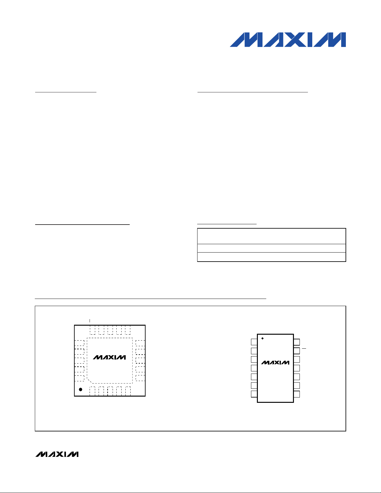
Pin Configurations
19-3942; Rev 0; 1/06
For pricing, delivery, and ordering information, please contact Maxim/Dallas Direct! at
1-888-629-4642, or visit Maxim’s website at www.maxim-ic.com.
PART
PINPACKAGE
PKG
CODE
MAX9491ETP
T2055-5
14 TSSOP U14-2
Ordering Information
*Future product—contact factory for availability.
**EP = Exposed pad.
TEMP RANGE
-40°C to +85°C 20 TQFN-EP**
MAX9491EUD* -40°C to +85°C
DD
I.C.
V
DDA
V
AGND
DD
V
GND
GND
11
5
CLK_OUT
TOP VIEW
X1
I.C.
I.C.
TUNE
GND
1
2
3
4
DD
MAX9491
5
6
7
TSSOP
GND
10
I.C.
9
I.C.
8
7
I.C.
6
I.C.
CLK_OUT
14
X2
13
PD
12
V
DD
11
GNDV
10
I.C.
9
GND
8
I.C.
TOP VIEW
V
DD
X2
X1
I.C.
PD
15 14 13 12
16
17
18
19
20I.C.
MAX9491
1234
TUNE
TQFN (5mm x 5mm)
Page 2
MAX9491
Factory Programmable Single PLL
Clock Generator
2 _______________________________________________________________________________________
ABSOLUTE MAXIMUM RATINGS
DC ELECTRICAL CHARACTERISTICS
(VDD= V
DDA
= +3.0V to +3.6V and TA= -40°C to +85°C. Typical values at VDD= V
DDA
= 3.3V, TA= +25°C, unless otherwise noted.)
(Note 1)
Stresses beyond those listed under “Absolute Maximum Ratings” may cause permanent damage to the device. These are stress ratings only, and functional
operation of the device at these or any other conditions beyond those indicated in the operational sections of the specifications is not implied. Exposure to
absolute maximum rating conditions for extended periods may affect device reliability.
VDDto GND...........................................................-0.3V to +4.0V
V
DDA
to AGND ......................................................-0.3V to +4.0V
All Other Pins to GND ..................................-0.3V to V
DD
+ 0.3V
Short-Circuit Duration
(all LVCMOS outputs)..............................................Continuous
ESD Protection (Human Body Model)..................................±2kV
Continuous Power Dissipation (T
A
= +70°C)
20-Lead TQFN (derate 21.3mW/°C above +70°C) ....2758mW
14-Pin TSSOP (derate 9.1mW/°C above +70°C) ......796.8mW
Storage Temperature Range .............................-65°C to +150°C
Maximum Junction Temperature .....................................+150°C
Operating Temperature Range ...........................-40°C to +85°C
Lead Temperature (soldering, 10s) .................................+300°C
LVCMOS INPUTS (PD, X1 as a reference INPUT CLK)
Input High Level V
Input Low Level V
High-Level Input Current I
Low-Level Input Current I
CLOCK OUTPUT (CLK_OUT)
Output High Level V
Output Low Level V
POWER SUPPLIES
Digital Power-Supply Voltage V
Analog Power-Supply Voltage V
Total Current for Digital and
Analog Supplies
Power-Down Current IDC2 PD = low 60 µA
PARAMETER SYMBOL CONDITIONS MIN TYP MAX UNITS
IH
IL
IH
OH
DD
DDA
I
DC
VIN = V
DD
VIN = 0 -20 µA
IL
IOH = -4mA
IOL = 4mA 0.4 V
OL
f
= 45MHz, no load
OUT
= 13MHz
f
IN
2.0 V
0 0.8 V
V
-
DD
0.6
3.0 3.6 V
3.0 3.6 V
10 mA
DD
20 µA
V
V
Page 3
MAX9491
Factory Programmable Single PLL
Clock Generator
_______________________________________________________________________________________ 3
AC ELECTRICAL CHARACTERISTICS
(VDD= V
DDA
= +3.0V to +3.6V, CL= 10pF and TA= -40°C to +85°C. Typical values are at VDD= V
DDA
= 3.3V, TA= +25°C, unless
otherwise noted.) (Note 2)
Note 1: All parameters are tested at TA= +25°C. Specifications over temperature are guaranteed by design and characterization.
Note 2: Guaranteed by design and characterization; limits are set at ±6 sigma.
OUTPUT CLOCK (CLK_OUT)
Minimum Frequency Range f
Maximum Frequency Range
Clock Rise Time t
Clock Fall Time t
Duty Cycle f
Soft Power-On Time t
Hard Power-On Time t
VCXO CLOCK
Crystal Frequency f
Crystal Accuracy ±30 ppm
Tuning Voltage Range V
VCXO Tuning Range V
TUNE Input Impedance Z
Output CLK Accuracy V
PARAMETER SYMBOL CONDITIONS MIN TYP MAX UNITS
= 5MHz to 50MHz 4
f
OUT
R
F
PO2
PO1
XTL
TUNE
TUNE
IN
CL < 5pF 133 200
20% to 80% of VDD, f
= 13MHz
f
IN
80% to 20% of VDD, f
= 13MHz
f
IN
= 45MHz, fIN = 13MHz 44 50 56 %
OUT
f
= 45MHz, fIN = 13MHz 14
OUT
f
= 80MHz, fIN = 13MHz 22Output Period Jitter J
OUT
P
f
= 197MHz, fIN = 13MHz 13
OUT
PD from low to high, f
f
= 13MHz, see Figure 2
IN
See Figure 2 15 ms
= 0 to 3V, C1 = C2 = 4pF ±150 ±200 ppm
TUNE
= 1.5V, C1 = C2 = 4pF ±50 ppm
TUNE
OUT
OUT
OUT
= 80MHz,
= 80MHz,
= 45MHz,
1.5 ns
1.3 ns
1ms
27 MHz
03V
95 kΩ
MHz
ps
RMS
Page 4
MAX9491
Factory Programmable Single PLL
Clock Generator
4 _______________________________________________________________________________________
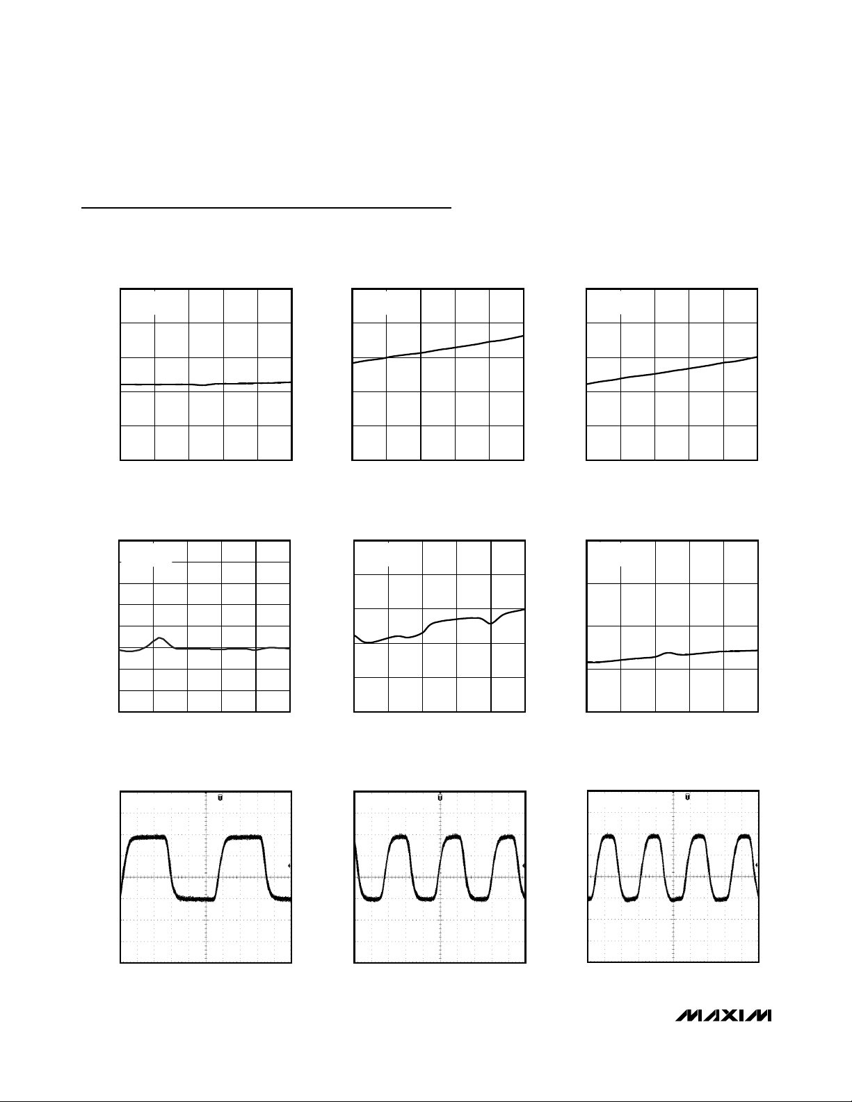
Typical Operating Characteristics
(VDD= V
DDA
= +3.3V, TA= +25°C, fIN= 13MHz clock, CL= 10pF, 27MHz, unless otherwise noted.)
SUPPLY CURRENT vs. TEMPERATURE
13
fIN = 13MHz
= 45MHz
f
OUT
12
11
10
SUPPLY CURRENT (mA)
9
8
-40 10-15 35 60 85
TEMPERATURE (°C)
JITTER vs. TEMPERATURE
40
fIN = 13MHz
= 45MHz
f
OUT
35
30
25
20
JITTER (ps)
15
10
5
0
-40 10-15 35 60 85
TEMPERATURE (°C)
MAX9491 toc01
MAX9491 toc04
RISE TIME vs. TEMPERATURE
2.2
fIN = 13MHz
= 45MHz
f
OUT
1.8
1.4
1.0
RISE TIME (ns)
0.6
0.2
-40 10-15 35 60 85
TEMPERATURE (°C)
JITTER vs. TEMPERATURE
40
fIN = 13MHz
= 80MHz
f
OUT
32
24
JITTER (ps)
16
8
0
-40 10-15 35 60 85
TEMPERATURE (°C)
MAX9491 toc02
MAX9491 toc05
FALL TIME vs. TEMPERATURE
2.2
fIN = 13MHz
= 45MHz
f
OUT
1.8
1.4
1.0
FALL TIME (ns)
0.6
0.2
-40 10-15 35 60 85
TEMPERATURE (°C)
JITTER vs. TEMPERATURE
40
fIN = 27MHz
= 197MHz
f
OUT
30
20
JITTER (ps)
10
0
-40 10-15 35 60 85
TEMPERATURE (°C)
MAX9491 toc03
MAX9491 toc06
TYPICAL CLK_OUT WAVEFORM AT 45MHz
VDD = V
= 3.0V
DDA
4ns/div
MAX9491 toc07
CLK1
1V/div
TYPICAL CLK_OUT WAVEFORM AT 80MHz
VDD = V
= 3.0V
DDA
4ns/div
MAX9491 toc08
CLK1
1V/div
TYPICAL CLK_OUT WAVEFORM AT 197MHz
VDD = V
= 3.0V
DDA
4ns/div
MAX9491 toc09
CLK1
1V/div
Page 5

MAX9491
Factory Programmable Single PLL
Clock Generator
_______________________________________________________________________________________ 5
Typical Operating Characteristics (continued)
(VDD= V
DDA
= +3.3V, TA= +25°C, fIN= 13MHz clock, CL= 10pF, 27MHz, unless otherwise noted.)
VCXO ACCURACY vs. VCXO TUNING RANGE
300
fIN = 27MHz
= 45MHz
f
OUT
200
100
0
-100
VCXO ACCURACY (PP/M)
-200
-300
0 1.0 1.50.5 2.0 2.5 3.0
VCXO TUNING RANGE (V)
6pF
5pF
45MHz OUTPUT
10dB/REF = 0dBm
RBW = 3kHz
VBW = 3kHz
ATN = 20dB
CENTER = 45MHz
SPAN = 2MHz
4pF
MAX9491 toc10
MAX9491 toc12
DUTY CYCLE vs. OUTPUT FREQUENCY
100
fIN = 13MHz
80
60
40
DUTY CYCLE (%)
20
0
45 5550 60 65 70 75 80
FREQUENCY (MHz)
80MHz OUTPUT
10dB/REF = 0dBm
RBW = 3kHz
VBW = 3kHz
ATN = 20dB
CENTER = 80MHz
SPAN = 2MHz
MAX9491 toc11
MAX9491 toc13
Page 6

MAX9491
Factory Programmable Single PLL
Clock Generator
6 _______________________________________________________________________________________
Detailed Description
The MAX9491 features a programmable fractional-N
PLL, so frequencies between 4MHz to 200MHz can be
generated. The device provides a buffered PLL clock
output. The crystal input frequency can be between
5MHz and 35MHz, and the clock input between 5MHz
and 50MHz. The internal VCXO has a fine-tuning range
of ±200ppm.
Power-Down
Driving PD low places the MAX9491 in power-down
mode. PD then sets CLK_OUT to high impedance and
shuts down the PLL. CLK_OUT has an 80kΩ (typ) internal pulldown resistor.
Voltage-Controlled Crystal Oscillator
(VCXO)
The MAX9491’s internal VCXO produces a reference
clock for the PLL used to generate the CLK_OUT. The
oscillator uses a crystal as the base frequency reference and has a voltage-controlled tuning input for micro
adjustment in a ±200ppm range. The tuning voltage,
V
TUNE
, can vary from 0 to 3V as shown in Figure 1. The
crystal should be AT-cut and oscillate on its fundamental mode with ±30ppm. The crystal shunt capacitor
Pin Description
Typical Operating Circuit/Block Diagram
+3.3V
0.1µF
V
DDA
X1
OR REFERENCE
INPUT
PIN
TQFN TSSOP
1 5 TUNE
2—V
3 — AGND Analog Ground
4, 10, 11 6, 9, 11 GND Ground
5 7 CLK_OUT Output Clock. Internally pulled down.
6–9, 14, 19, 20 2, 3, 8, 10 I.C. Internally Connected. Leave unconnected for normal operation.
12, 13, 16 4, 12 V
15 13 PD
17 14 X2 Crystal Connection 2. Leave unconnected if using a reference clock.
18 1 X1 Crystal Connection 1 or Reference Clock Input
EP — EP Exposed Paddle (TQFN Only). Connect EP to GND or leave unconnected.
NAME FUNCTION
DDA
DD
C1
C2
X2
TUNE
AGND
GND
VCXO Tune Voltage Input. If using a reference clock input or VCXO is not used,
connect TUNE to V
Analog Power Supply. Bypass to GND with a 0.1µF capacitor.
Power Supply. Bypass to GND with a 0.1µF capacitor.
Active-Low Power-Down Input. Pull high for normal operation. Drive PD low to place
MAX9491 in power-down mode. Internally pulled down.
VCXO
DD
MAX9491
PLL
CLK_OUT
OTP
.
+3.3V
V
DD
V
DD
V
DD
PD
0.1µF x 3
Page 7

MAX9491
Factory Programmable Single PLL
Clock Generator
_______________________________________________________________________________________ 7
should be less than 10pF, including board parasitic
capacitance. To achieve up to ±200ppm pullability, make
sure the crystal-loading capacitance is less than 14pF.
The VCXO is a free-running oscillator. It starts oscillating
with an internal POR signal and can be disabled by PD.
When VCXO is not used, connect TUNE to V
DD
.
Applications Information
Using an Input Clock as the Reference
When an input clock is used as the reference, connect
the input clock to X1, leave X2 unconnected, and connect
TUNE to VDD.
Crystal Selection
When using a crystal with the MAX9491’s internal oscillator, connect the crystal to X1 and X2. Choose an ATcut crystal that oscillates on its fundamental mode with
±30ppm and loading capacitance less than 14pF. To
achieve a wide VCXO tuning range, select a crystal
with motional capacitance greater than 7fF and connect 6pF or less shunt capacitors at both X1 and X2 to
ground. When the VCXO is used as an oscillator, select
both shunt capacitors to approximately 13pF. The optimal shunt capacitors for achieving minimum frequency
offset can be determined experimentally.
Figure 1. VCXO Tuning Range for a 27MHz Crystal
Figure 2. PLL Settling Time
27.0405
+150ppm
(MHz)
VCXO OUTPUT FREQUENCY
26.99595
27.00
-150ppm
0
3V V
TUNE
V
DD
2.2V
CLK_IN
PD
CLK_OUT
t
t
PO1
t
PO2
Page 8

MAX9491
Factory Programmable Single PLL
Clock Generator
8 _______________________________________________________________________________________
Board Layout Considerations and
Bypassing
The MAX9491’s high-frequency oscillator requires
proper layout to ensure stability. For best performance,
place components as close as possible to the device.
Digital or AC transient signals on GND can create noise
at the clock output. Return GND to the highest quality
ground available. Bypass each V
DD
and V
DDA
with a
0.1µF capacitor, placed as close as possible to the
device. Careful PC board ground layout minimizes
crosstalk between the output and digital inputs.
Chip Information
PROCESS: CMOS
Page 9

MAX9491
Factory Programmable Single PLL
Clock Generator
_______________________________________________________________________________________ 9
Package Information
(The package drawing(s) in this data sheet may not reflect the most current specifications. For the latest package outline information,
go to www.maxim-ic.com/packages
.)
TSSOP4.40mm.EPS
PACKAGE OUTLINE, TSSOP 4.40mm BODY
21-0066
1
G
1
Page 10

MAX9491
Factory Programmable Single PLL
Clock Generator
10 ______________________________________________________________________________________
Package Information (continued)
(The package drawing(s) in this data sheet may not reflect the most current specifications. For the latest package outline information,
go to www.maxim-ic.com/packages
.)
MARKING
PIN # 1
I.D.
C
D
AAAAA
D2
C
L
D/2
E/2
E
e
L
L1
0.10 C
A
0.08 C
A3
A1
(NE-1) X e
DETAIL A
k
L
D2/2
e
(ND-1) X e
L
e e
b
0.10 M C A B
L
E2/2
C
E2
L
DETAIL B
PIN # 1 I.D.
0.35x45°
CC
L
e/2
QFN THIN.EPS
L
PACKAGE OUTLINE,
16, 20, 28, 32, 40L THIN QFN, 5x5x0.8mm
-DRAWING NOT TO SCALE-
21-0140
1
I
2
Page 11

MAX9491
Factory Programmable Single PLL
Clock Generator
Maxim cannot assume responsibility for use of any circuitry other than circuitry entirely embodied in a Maxim product. No circuit patent licenses are
implied. Maxim reserves the right to change the circuitry and specifications without notice at any time.
Maxim Integrated Products, 120 San Gabriel Drive, Sunnyvale, CA 94086 408-737-7600 ____________________ 11
© 2006 Maxim Integrated Products Printed USA is a registered trademark of Maxim Integrated Products, Inc.
Package Information (continued)
(The package drawing(s) in this data sheet may not reflect the most current specifications. For the latest package outline information,
go to www.maxim-ic.com/packages
.)
Springer
20L 5x5
NOM.
0.75
0.02
0.30
5.00
5.00
0.65 BSC.
0.55
20
5
5
WHHC
MAX.
0.80
0.05
0.35
5.10
5.10
0.65
--
MIN.
0.70
0.20
4.90
4.90
0.25
0.45
28L 5x5
NOM.
0.75
0
0.02
0.20 REF.
0.25
5.00
5.00
0.50 BSC.
0.55
---
28
7
7
WHHD-1
MAX.
MIN.
0.80
0.70
0.05
0.30
0.20 0.25 0.30
5.10
4.90
5.10
4.90
--
0.25
0.65
0.30
32L 5x5
NOM.
0.75
0
0.02
0.20 REF.
5.00
5.00
0.50 BSC.
0.40
---
WHHD-2
32
8
8
MAX.
MIN.
0.70
0.80
0.05
0.15
5.10
4.90
5.10
4.90 5.00
--
0.25 0.35 0.45
0.50
0.30
40L 5x5
NOM.
0.75 0.80
0.20 REF.
5.00 5.10
0.40 BSC.
0.40 0.50
40
10
10
-----
EXPOSED PAD VARIATIONS
MAX.
0.050 0.02
0.250.20
5.10
PKG.
CODES
T1655-2
T2055-4
D2
NOM.MIN.
T2855-3 3.15 3.25 3.35 3.15 3.25 3.35
T2855-4 2.60 2.70 2.80 2.60 2.70 2.80
0.600.40 0.50
T2855-5 2.60 2.70 2.80 2.60 2.70 2.80
T2855-6
3.15 3.25 3.35 3.15 3.25 3.35
T2855-7 2.60 2.70
3.15
T2855N-1
3.25 3.15 3.25 3.35
3.00 3.10T3255-3 3 3.203.00 3.10
T3255-5 YES3.003.103.00
3.30T4055-1 3.20 3.40 3.20 3.30 3.40
PACKAGE OUTLINE,
16, 20, 28, 32, 40L THIN QFN, 5x5x0.8mm
DOWN
E2
NOM. MAX.
MIN.
MAX.
3.203.00T1655-3 3.10 3.00 3.10 3.20 NO
3.103.00 3.203.103.00 3.20
3.353.15T2055-5 3.25 3.15 3.25 3.35
2.80
2.60 2.70 2.80
3.353.15T2855-8 3.25 3.15 3.25 3.35
3.35
3.20
3.203.00 3.10T3255-4 3 3.203.00 3.10
3.20
3.203.10T3255N-1 3.00
SEE COMMON DIMENSIONS TABLE
**
21-0140
L
exceptions
BONDS
±0.15
ALLOWED
YES3.203.103.003.103.00 3.20
**
**
NO3.203.103.003.10T1655N-1 3.00 3.20
**
YES3.103.00 3.203.103.00 3.20T2055-3
**
NO
**
YES
0.40
YES
**
YES
**
NO
**
NO
**
YES
**
0.40
YES
NO
**
YES
**
NO
**
3.203.10
**
3.203.103.00
NO
**
YES
**
I
2
2
COMMON DIMENSIONS
PKG.
SYMBOL
JEDEC
NOTES:
10. WARPAGE SHALL NOT EXCEED 0.10 mm.
11. MARKING IS FOR PACKAGE ORIENTATION REFERENCE ONLY.
12. NUMBER OF LEADS SHOWN ARE FOR REFERENCE ONLY.
13. LEAD CENTERLINES TO BE AT TRUE POSITION AS DEFINED BY BASIC DIMENSION "e", ±0.05.
-DRAWING NOT TO SCALE-
16L 5x5
MIN. MAX.NOM.
A
0.70 0.800.75
A1
A3
0.20 REF.
b
0.25
D
4.90
E
4.90
e
0.80 BSC.
0.250--
k
L
0.30 0.500.40
L1
---
N
ND
NE
WHHB
1. DIMENSIONING & TOLERANCING CONFORM TO ASME Y14.5M-1994.
2. ALL DIMENSIONS ARE IN MILLIMETERS. ANGLES ARE IN DEGREES.
3. N IS THE TOTAL NUMBER OF TERMINALS.
4. THE TERMINAL #1 IDENTIFIER AND TERMINAL NUMBERING CONVENTION SHALL
CONFORM TO JESD 95-1 SPP-012. DETAILS OF TERMINAL #1 IDENTIFIER ARE
OPTIONAL, BUT MUST BE LOCATED WITHIN THE ZONE INDICATED. THE TERMINAL #1
IDENTIFIER MAY BE EITHER A MOLD OR MARKED FEATURE.
5. DIMENSION b APPLIES TO METALLIZED TERMINAL AND IS MEASURED BETWEEN
0.25 mm AND 0.30 mm FROM TERMINAL TIP.
6. ND AND NE REFER TO THE NUMBER OF TERMINALS ON EACH D AND E SIDE RESPECTIVELY.
7. DEPOPULATION IS POSSIBLE IN A SYMMETRICAL FASHION.
8. COPLANARITY APPLIES TO THE EXPOSED HEAT SINK SLUG AS WELL AS THE TERMINALS.
9. DRAWING CONFORMS TO JEDEC MO220, EXCEPT EXPOSED PAD DIMENSION FOR
T2855-3 AND T2855-6.
0.02
5.00
16
MIN.
0.70
0.05
0
0.20 REF.
0.25
0.350.30
4.90
5.10
4.90
5.105.00
0.25
0.45
---
4
4
 Loading...