

Page 1
General Description
The MAX9489 clock generator provides multiple clock
outputs, ideal for network routers. The MAX9489 provides 15 buffered clock outputs, each independently
programmable to any of 10 individual frequencies:
133MHz, 125MHz, 100MHz, 83MHz, 80MHz, 66MHz,
62.5MHz, 50MHz, 33MHz, or 25MHz. All of the outputs
are single-ended LVCMOS. The MAX9489 is controlled
through its I2C™ interface.
At power-up, the frequency of output CLK1 is set by the
tri-level input SEL to 100MHz, 125MHz, or 133MHz,
while all other outputs are logic low. All outputs are then
programmable to any available frequency through the
I2C interface. Additionally, all output frequencies are
adjustable up or down, by a margin of 5% or 10%,
through the I
2
C interface.
The MAX9489 requires a 25MHz reference that can be
either a crystal or an external clock signal. The
MAX9489 requires a +3.0V to +3.6V power supply and
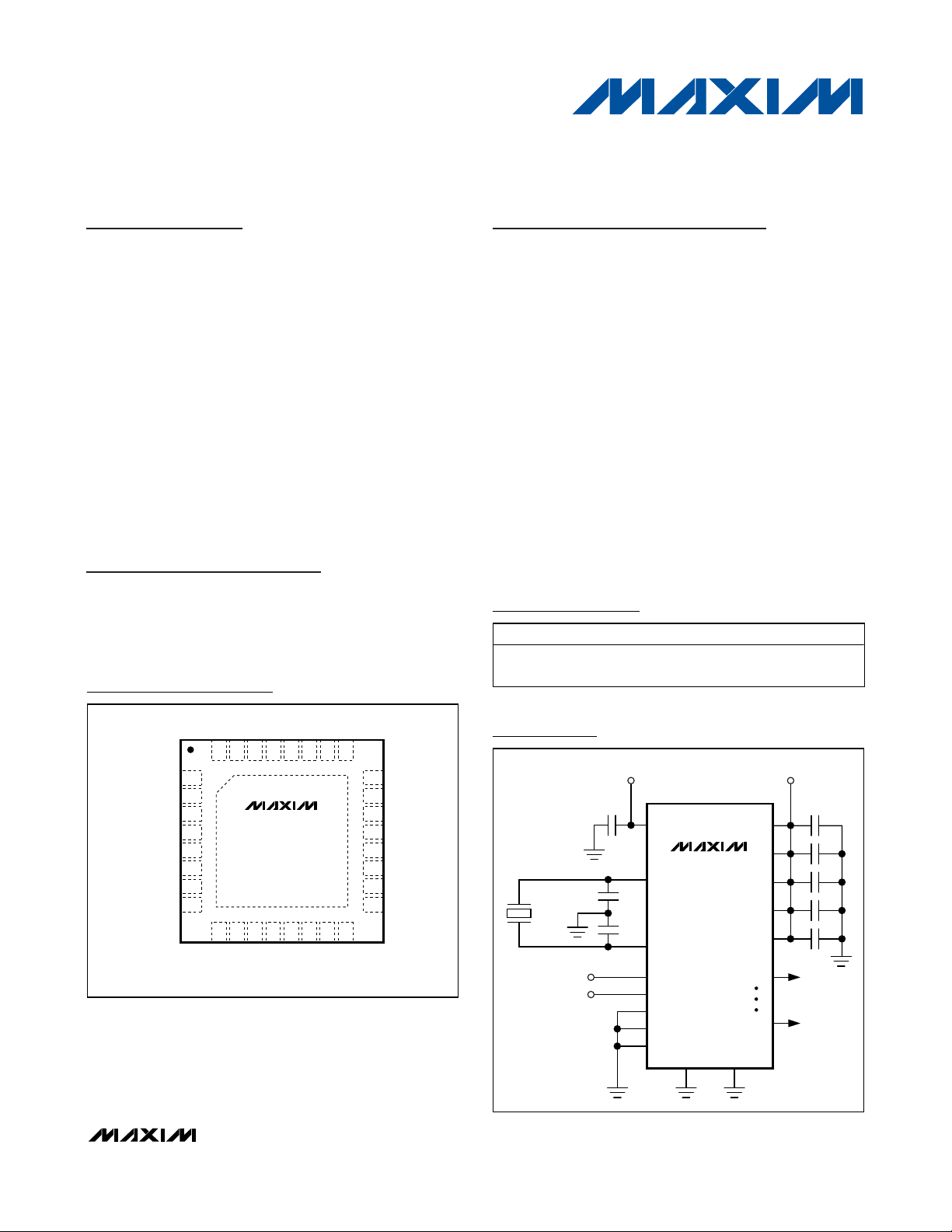
is available in a 32-pin thin QFN package with an
exposed pad for heat removal.
Applications
Network Routers
Telecom/Networking Equipment
Storage Area Networks/Network Attached
Storage
Features
♦ 15 LVCMOS Outputs with 10 Independently
Programmable Frequencies: 133MHz, 125MHz,
100MHz, 83MHz, 80MHz, 66MHz, 62.5MHz, 50MHz,
33MHz, and 25MHz
♦ 25MHz Crystal or Clock Input Reference
♦ Programmable Through I
2
C Interface
♦ Programmable Output Frequency Margin of ±5%
or ±10%
♦ Pin-Selectable Power-Up Frequency for CLK1
Output: 100MHz, 125MHz, or 133MHz
♦ Low Output Period Jitter: < 48ps
RMS
♦ Output-to-Output Skew < 200ps
♦ Available in 32-Lead, 5mm x 5mm x 0.8mm,
Thin QFN Package
♦ Operates from +3.0V to +3.6V Power Supply
♦ Power Dissipation 450mW (typ)
♦ Extended Temperature Range: -40°C to +85°C
MAX9489
Multiple-Output Network Clock Generator
________________________________________________________________ Maxim Integrated Products 1
Ordering Information
19-3385; Rev 0; 8/04
For pricing, delivery, and ordering information, please contact Maxim/Dallas Direct! at
1-888-629-4642, or visit Maxim’s website at www.maxim-ic.com.
Pin Configuration
MAX9489
25MHz
10pF
10pF
X1
AV
DD
X2
SDA
0.1µF
SCL
SA0
SA1
SEL
AGND
GND
CLK15
CLK1
V
DD
V
DD
V
DD
V
DD
V
DD
+3.3V +3.3V
SERIAL
INTERFACE
CLOCK
OUTPUTS
0.1µF x 5
Typical Operating Circuit
I2C is a trademark of Philips Corp.
Purchase of I
2
C components of Maxim Integrated Products, Inc.,
or one of its sublicensed Associated Companies, conveys a
license under the Philips I
2
C Patent Rights to use these compo-
nents in an I
2
C system, provided that the system conforms to the
I
2
C Standard Specification as defined by Philips.
*EP = Exposed pad.
TOP VIEW
DD
V
32
SA131SA030GND29V
28
DD
CLK1527CLK1426CLK13
25
PART TEMP RANGE PIN-PACKAGE
MAX9489ETJ -40°C to +85°C
32 Thin QFN-EP*
5mm x 5mm x 0.8mm
24
GND 1
SCL
2
SDA
3
SEL
4
AV
5
DD
X1
6
X2
AGND
7
8
MAX9489
EXPOSED PAD (GND)
12
DD
V
CLK413CLK514CLK6
15
16
11
CLK19CLK210CLK3
THIN QFN-EP
V
DD
CLK12
23
CLK11
22
CLK10
21
V
20
DD
CLK9
19
CLK8
18
CLK7
17
DD
V
Page 2
MAX9489
Multiple-Output Network Clock Generator
2 _______________________________________________________________________________________
ABSOLUTE MAXIMUM RATINGS
DC ELECTRICAL CHARACTERISTICS
(VDD= AVDD= +3.0V to +3.6V, TA= -40°C to +85°C, unless otherwise noted. Typical values are at VDD= AVDD= +3.3V, TA= +25°C.)
(Note 1)
Stresses beyond those listed under “Absolute Maximum Ratings” may cause permanent damage to the device. These are stress ratings only, and functional
operation of the device at these or any other conditions beyond those indicated in the operational sections of the specifications is not implied. Exposure to
absolute maximum rating conditions for extended periods may affect device reliability.
VDDto GND ..............................................…….….-0.3V to +4.0V
AGND to GND .............................................……...-0.3V to +0.3V
All Other Pins to GND.................................-0.3V to (V
DD
+ 0.3V)
Short-Circuit Duration for all CLK_ Outputs ...............Continuous
Continuous Power Dissipation (T
A
= +70°C)
32-Pin Thin QFN (derate 21.3mW/°C above +70°C) ....1702mW
Storage Temperature Range .............................-65°C to +150°C
Maximum Junction Temperature .....................................+150°C
Operating Temperature Range ...........................-40°C to +85°C
ESD Rating (Human Body Model) .......................................±2kV
Lead Temperature (soldering, 10s) .................................+300°C
PARAMETER SYMBOL CONDITIONS MIN TYP MAX UNITS
CLOCK INPUT (X1)
Input High Level V
Input Low Level V
Input Current I
CLOCK OUTPUTS (CLK_)
Output High Level V
Output Low Level V
Output Short-Circuit Current I
Output Capacitance C
TRI-LEVEL INPUTS (SEL, SA0, SA1)
Input High Level V
Input Low Level V
Input Open Level V
Input Current I
SERIAL INTERFACE (SCL, SDA) (Note 3)
Input High Level V
Input Low Level V
Input leakage Current IIH, I
Low-Level Output V
Input Capacitance Ci (Note 2) 10 pF
IL1
IL2
IH1
IL1
, I
IH1 VX
OH
OL
OS
O
IH2
IL2
IO2
, I
IH2
IH
IL
IL
OL
_ = 0 to V
IOH = -100µA
IOH = -4mA 2.4
IOH = -8mA 2.1
IOL = 100µA 0.2
IOL = 4mA 0.4
IOL = 8mA 0.75
CLK_ = VDD or GND 45 mA
(Note 2) 5 pF
V
= 0 or V
IL2
I
= 4mA 0 0.4 V
SINK
2.0 V
0.8 V
DD
-5 +5 µA
V
-
DD
0.2
2.5 V
0.8 V
1.35 1.90 V
IH2
= V
DD
-10 +10 µA
0.7 x
V
DD
0
V
0.3 x
V
-1 +1 µA
DD
DD
V
V
V
V
Page 3
MAX9489
Multiple-Output Network Clock Generator
_______________________________________________________________________________________ 3
DC ELECTRICAL CHARACTERISTICS (continued)
(VDD= AVDD= +3.0V to +3.6V, TA= -40°C to +85°C, unless otherwise noted. Typical values are at VDD= AVDD= +3.3V, TA= +25°C.)
(Note 1)
AC ELECTRICAL CHARACTERISTICS
(VDD= AVDD= +3.0V to +3.6V, CL= 10pF, unless otherwise noted. Typical values are at VDD= AVDD= +3.3V, TA= +25°C, with all
CLK_ outputs at 133MHz.) (Note 2)
POWER SUPPLIES
Digital Power-Supply Voltage V
Analog Power-Supply Voltage AV
Total Supply Current C L = 10p f ( w i th al l C LK_ outp uts at 133M H z) 134 160 mA
Total Power-Down Current I
PARAMETER SYMBOL CONDITIONS MIN TYP MAX UNITS
DD
PD
DD
All clock registers = 0x00 38 47 mA
3.0 3.6 V
3.0 3.6 V
PARAMETER SYMBOL CONDITIONS MIN TYP MAX UNITS
OUTPUTS (CLK_)
Crystal Frequency Tolerance ∆f
Output-to-Output Skew t
Rise Time t
Fall Time t
Duty Cycle 40 60 %
Output Period Jitter J
Power-Up Time t
PLL Lockup Time t
Margin Accuracy Select ±5% or ±10% margin -1 +1 %
A
SKO
R1
F1
P
PO
Lock
Any two CLK_ outputs 200 ps
20% VDD to 80% V
80% VDD to 20% V
RMS 53 ps
VDD > 2.8V to PLL lock 2 ms
PLL dividing ratio set to PLL lock 20 µs
DD
DD
-50 +50 ppm
1.8 2.5 ns
1.8 2.5 ns
Page 4
MAX9489
Multiple-Output Network Clock Generator
4 _______________________________________________________________________________________
Note 1: All DC parameters tested at TA= +25°C. Specifications over temperature are guaranteed by design.
Note 2: Guaranteed by design.
Note 3: No high output level is specified but only the output resistance to the bus. For I
2
C, the high-level voltage is provided by
pullup resistors on the bus.
Note 4: A master device must provide a hold time of at least 300ns for the SDA signal (referred to V
IL
of the SCL signal) to bridge
the undefined region of SCL’s falling edge.
Note 5: C
b
= total capacitance of one bus line in pF. tRand tFmeasured between 0.3(VDD) and 0.7(VDD).
Note 6: Input filters on the SDA and SCL inputs suppress noise spikes less than 50ns.
SERIAL INTERFACE TIMING
(VDD= AVDD= +3.3V, TA= -40°C to +85°C.) (Note 1, Figure 2)
PARAMETER SYMBOL CONDITIONS MIN TYP MAX UNITS
Serial Clock f
Bus Free Time Between STOP
and START Conditions
Hold Time, Repeated START
Condition
Repeated START Condition
Setup Time
STOP Condition Setup Time t
Data Hold Time Master t
Data Hold Time Slave t
Data Setup Time t
SCL Clock Low Period t
SCL Clock High Period t
Rise Time of SDA and SCL,
Receiving
Fall Time of SDA and SCL,
Receiving
Fall Time of SDA, Transmitting t
Pulse Width of Spike Suppressed t
Capacitive Load for Each Bus
Line
SCL
t
BUF
t
HD,STA
t
SU,STA
SU,STO
HD,DAT
HD,DAT
SU,DAT
LOW
HIGH
t
R
t
F
F,TX
SP
C
b
1.3 µs
0.6 µs
0.6 µs
0.6 µs
(Note 4) 15 900 ns
(Note 4) 15 900 ns
100 ns
1.3 µs
0.7 µs
(Notes 2, 5)
(Notes 2, 5)
(Notes 2, 5)
(Notes 2, 6) 0 50 ns
(Note 2) 400 pF
20 +
0.1C
20 +
0.1C
20 +
0.1C
b
b
b
400 kHz
300 ns
300 ns
250 ns
Page 5

MAX9489
Multiple-Output Network Clock Generator
_______________________________________________________________________________________ 5
Typical Operating Characteristics
(VDD= 3.3V, TA= +25°C, unless otherwise noted.)
SUPPLY CURRENT
vs. TEMPERATURE
MAX9489 toc01
TEMPERATURE (°C)
SUPPLY CURRENT (mA)
603510-15
110
120
130
140
150
160
100
-40 85
RISE AND FALL TIMES
vs. TEMPERATURE
MAX9489 toc02
TEMPERATURE (°C)
TRANSITION TIME (ns)
603510-15
1.2
1.4
1.7
1.9
2.3
2.1
1.0
-40 85
t
FALL
t
RISE
JITTER vs. TEMPERATURE
MAX9489 toc03
TEMPERATURE (°C)
RMS PERIOD JITTER (ps)
603510-15
10
20
30
40
50
60
70
0
-40 85
133MHz
25MHz
JITTER vs. FREQUENCY
MAX9489 toc04
FREQUENCY (MHz)
RMS PERIOD JITTER (ps)
11597796143
15
30
45
60
75
0
25 133
TYPICAL CLOCK WAVEFORMS
MAX9489 toc05
10ns/div
A
B
A: 100MHz, 100mV/div
B: 25MHz, 100mV/div
Page 6
MAX9489
Multiple-Output Network Clock Generator
6 _______________________________________________________________________________________
Pin Description
PIN NAME FUNCTION
1, 29 GND Digital Ground
2 SCL Serial Clock Input. Serial interface clock.
3 SDA Serial Data I/O. Data I/O of serial interface.
4 SEL
5AVDDPower-Supply Input for Analog Circuits
6X1
7X2
8 AGND Analog GND
9 CLK1 Clock 1 Output
10 CLK2 Clock 2 Output
11 CLK3 Clock 3 Output
12, 16, 20,
24, 28, 32
13 CLK4 Clock 4 Output
14 CLK5 Clock 5 Output
15 CLK6 Clock 6 Output
17 CLK7 Clock 7 Output
18 CLK8 Clock 8 Output
19 CLK9 Clock 9 Output
21 CLK10 Clock 10 Output
22 CLK11 Clock 11 Output
23 CLK12 Clock 12 Output
25 CLK13 Clock 13 Output
26 CLK14 Clock 14 Output
27 CLK15 Clock 15 Output
30 SA0
31 SA1
EP — Exposed pad. Connect to GND.
V
DD
Frequency Select for CLK1. Selects the frequency for CLK1 at power-up. SEL is a tri-level input. Force
SEL high for CLK1 = 100MHz. Leave SEL open for CLK1 = 125MHz. Force SEL low for CLK1 = 133MHz.
Crystal Connection or Clock Input. If using a 25MHz crystal, connect it to X1 and X2. If using a reference
clock, connect the clock signal to X1, and leave X2 floating. See the Typical Operating Circuit.
Power-Supply Input for Digital Circuits
Address-Select Inputs for Serial Interface. SA0 and SA1 select the serial interface address, as shown in
Table 1. SA0 and SA1 are tri-level inputs, making nine possible address combinations.
Page 7

MAX9489
Multiple-Output Network Clock Generator
_______________________________________________________________________________________ 7
Detailed Description
The MAX9489 clock generator produces 15 clock signals, CLK1 through CLK15. Each output is programmable through control registers to any of 10 individual
frequencies: 133MHz, 125MHz, 100MHz, 83MHz,
80MHz, 66MHz, 62.5MHz, 50MHz, 33MHz, or 25MHz.
Additionally, the frequency of all outputs can be
changed ±5% or ±10% through the frequency-margin
control register. At power-up, the frequency of CLK1 is
pin programmable to 100MHz, 125MHz, or 133MHz,
and all other CLK outputs are logic low. The required
25MHz input reference frequency can be either a crystal or an external clock signal. Figure 1 shows the
MAX9489 functional block diagram.
The MAX9489 is programmed through its I2C serial
interface. The I
2
C address is selected with two, tri-level
inputs, allowing up to nine MAX9489 devices to share
the same I2C bus. Power-supply and logic interface
signals are +3.0V to +3.6V. The operating state of the
MAX9489 is set by writing to the control registers, and
read by reading the control registers.
Reference Frequency Input
A reference frequency is required for the MAX9489.
The reference can be a 25MHz crystal or an external
clock signal. If using a 25MHz crystal, connect it across
X1 and X2, and connect 10pF capacitors from X1 and
X2 to GND (see the Typical Operating Circuit). If using
an external clock, connect the signal to X1 and leave
X2 floating.
Serial Interface
The MAX9489 is programmed through its I2C serial
interface. This interface has a clock, SCL, and a bidirectional data line, SDA. In an I2C system, a master,
typically a microcontroller, initiates all data transfers to
and from slave devices, and generates the clock to
synchronize the data transfers.
The MAX9489 operates as a slave device. The timing of
the SDA and SCL signals is detailed in Figure 2, the
Serial Interface Timing diagram. SDA operates as both
an input and an open-drain output. A pullup resistor,
typically 4.7kΩ, is required on SDA. SCL operates only
as an input. A pullup resistor, typically 4.7kΩ, is
required on SCL if there are multiple masters on the 2wire bus, or if the master in a single-master system has
an open-drain SCL output.
Bit Transfer
One data bit is transferred during each SCL clock
cycle. SDA must remain stable during the high period
of SCL, because changes in SDA while SCL is high are
START and STOP control signals. Both SDA and SCL
idle high.
START and STOP Conditions
A master signals the beginning of a transmission with a
START condition by transitioning SDA from high to low
while SCL is high (Figure 2). When communication is
complete, a master issues a STOP condition by transitioning SDA from low to high while SCL is high. The bus
is then free for another transmission.
Acknowledge Bits
After each 8 bits transferred, the receiving device generates an acknowledge signal by pulling SDA low for
the entire duration of the 9th clock pulse. If the receiving device does not pull SDA low, a not-acknowledge is
indicated (Figure 3).
Device Address
The MAX9489 has a 7-bit device address, pin configured by the two tri-level address inputs SA1 and SA0.
To select the device address, connect SA1 and SA0 to
V
DD
, GND, or leave open, as indicated in Table 1. The
MAX9489 has nine possible addresses, allowing up to
nine MAX9489 devices to share the same interface bus.
Figure 1. MAX9489 Functional Diagram
SEL
SCL
SDA
SA0
SA1
X1
25MHz
X2
OSC
AV
DD
I2C
400MHz
PLL1
400MHz
PLL2
3, 4, 5, 6, 12
2, 3, 4, 5, 10
MAX9489
DIVIDE BY
DIVIDE BY
V
DD
MUX
MUX
MUX
MUX
CLK1
CLK2
CLK14
CLK15
AGND GND
Page 8

MAX9489
Multiple-Output Network Clock Generator
8 _______________________________________________________________________________________
Writing to the MAX9489
Writing to the MAX9489 begins with a START condition
(Figures 3 and 4). Following the START condition, each
pulse on SCL transfers 1 bit of data. The first 7 bits
comprise the device address (see the Device Address
section). The 8th bit is low to indicate a write operation.
An acknowledge bit is then generated by the
MAX9489, signaling that it recognizes its address. The
next 8 bits form the register address byte (Table 2) and
determine which control register will receive the following data byte. The MAX9489 then generates another
acknowledge bit. The data byte is then written into the
addressed register of the MAX9489. An acknowledge
bit by the MAX9489 followed by a required STOP condition by the master complete the communication. To
write to the device again, repeat the entire write procedure; I2C burst write mode is not supported by the
MAX9489.
Reading the MAX9489 Setup
Reading from the MAX9489 registers begins with a
START condition and a device address with the write
bit set low, then the register address that is to be read,
followed by a repeated START condition and a device
address with the write bit set high, and finally the data
are shifted out (Figure 4). Following a START condition,
the first 7 bits comprise the device address. The 8th bit
is low to indicate a write operation (to write in the
following register address). An acknowledge bit is
then generated by the MAX9489, signaling that it recognizes its address. The next 8 bits form the register
address, indicating the location of the data to be read,
followed by another acknowledge, again generated by
the MAX9489. The master then produces a repeated
START condition and readdresses the device, this time
with the R/W bit high to indicate a read operation
(Figure 4). The MAX9489 generates an acknowledge
bit, signaling that it recognizes its address. The data
byte is then clocked out of the MAX9489. A final notacknowledge bit, generated by the master (not
required), and a STOP condition, also generated by the
master, complete the communication. To read from the
device again, the entire read procedure is repeated;
I2C burst read mode is not supported by the MAX9489.
Device Control Registers
The MAX9489 has 17 control registers. The register
addresses and functions are shown in Table 2. The first
16 registers are used to set the 15 outputs, with register
0x00 controlling all outputs simultaneously and the rest
mapped to individual outputs. Register 0x10 accesses
the frequency-margin control. All other addresses are
reserved and are not to be used.
Figure 2. Serial Interface Timing
Table 1. Device I2C Address Selection
SDA
t
SU, STA
t
HD, STA
t
SU, STO
SCL
t
LOW
t
SU, DAT
t
HD, DAT
t
BUF
t
HD, STA
START CONDITION
t
HIGH
t
R
t
F
PIN
SA1 SA0
Open V
Open GND 110 0100
Open Open 110 1000
GND V
GND GND 110 1001
GND Open 110 1100
V
DD
V
DD
V
DD
DD
DD
V
DD
GND 111 0010
Open 111 0001
DEVICE
ADDRESS
110 0010
111 0000
111 0100
REPEATED START CONDITION
START CONDITIONSTOP CONDITION
Page 9

MAX9489
Multiple-Output Network Clock Generator
_______________________________________________________________________________________ 9
Setting the Clock Frequencies
Each CLK_ output has an associated control register.
The contents of the registers determine the frequency
of their associated outputs. Table 3 provides the frequency mapping for the registers.
Example: To program CLK3 to 80MHz, first address the
device with R/W low, then send register address byte
0x03 followed by data byte 0x05 (Figure 5).
Frequency Margin Control
Frequency margin is controlled through control register
0x10. Table 4 provides the mapping for the available
margins. A selected margin applies to all outputs.
Example: To increase all clock outputs by 5%, address
the device, then send register address byte 0x10 followed by data byte 0x01.
Power Supply
The MAX9489 uses a 3.0V to 3.6V power supply connected to VDD, and 3.0V to 3.6V connected to AVDD.
Bypass each VDDat the device with a 0.1µF capacitor.
Also bypass AVDDat the device with a 0.1µF capacitor.
Additionally, use a bulk bypass capacitor of 10µF
where power enters the circuit board.
Board Layout Considerations
As with all high-frequency devices, board layout is
critical to proper operation. Place the crystal as close
as possible to X1 and X2, and minimize parasitic
capacitance around the crystal leads. Ensure that the
exposed pad makes good contact with GND.
Chip Information
TRANSISTOR COUNT: 15,219
PROCESS: CMOS
Figure 3. I2C Address and Acknowledge
Figure 4. I2C Interface Data Structure
SDA
SCL
START
MASTER-WRITE DATA STRUCTURE
START DEVICE ADDRESS REGISTER ADDRESS DATA IN STOPR/W
S 1 1 A4 A3 A2 A1 0 ACK RA7 RA6 RA5 RA4 RA3 RA2 RA1 RA0 ACK D7 D6 D5 D4 D3 D2 D1 D0 ACK P
MASTER-READ DATA STRUCTURE
START DEVICE ADDRESS REGISTER ADDRESSR/W
S 1 1 A4 A3 A2 A1 0 ACK RA7 RA6 RA5 RA4 RA3 RA2 RA1 RA0 ACK
S = START CONDITION
A_ = DEVICE ADDRESS
ACK = ACKNOWLEDGE
ACK = NOT ACKNOWLEDGE
1
MSB
RA_ = REGISTER ADDRESS
D_ = DATA
P = STOP CONDITION
RS = REPEATED START
1 A4 A3 A2 A1 A0 ACK
NOT ACKNOWLEDGE
R/W
LSB
DEVICE ADDRESS DATA OUT STOPR/W
RS 1 1 A4 A3 A2 A1 A0 1 ACK D7 D6 D5 D4 D3 D2 D1 D0 P
DATA DIRECTION
= MASTER TO SLAVE
= SLAVE TO MASTER
ACKNOWLEDGE
ACK
Page 10

MAX9489
Multiple-Output Network Clock Generator
10 ______________________________________________________________________________________
Table 2. Register Address Mapping
Table 3. Output Frequency Control
Table 4. Output Frequency Margin Control
*Power-up default for CLK2 through CLK15.
Figure 5. Example—Setting CLK3 to 80MHz
REGISTER ADDRESS BYTE REGISTER FUNCTION
0x00 Broadcast to all CLK registers
0x01 CLK1
0x02 CLK2
0x03 CLK3
0x04 CLK4
0x05 CLK5
0x06 CLK6
0x07 CLK7
0x08 CLK8
0x09 CLK9
0x0A CLK10
0x0B CLK11
0x0C CLK12
0x0D CLK13
0x0E CLK14
0x0F CLK15
0x10 Frequency margin control
0x11 – 0xFF Reserved, do not use
CLK_ REGISTER DATA
BYTE
0x00 Logic low*
0x01 133.3
0x02 125
0x03 100
0x04 83.3
0x05 80
0x06 66.6
0x07 62.5
0x08 50
0x09 33
0x0A 25
OUTPUT FREQUENCY
(MHz)
MARGIN REGISTER DATA
BYTE
0x00 0%
0x01 5%
0x02 10%
0x07 -5%
0x06 -10%
OUTPUT FREQUENCY
(MHz)
START DEVICE ADDRESS REGISTER ADDRESS DATA IN STOPR/W
S11A4A3A2A10ACK00000011ACK00000101ACKP
S = START CONDITION
A_ = DEVICE ADDRESS
ACK = ACKNOWLEDGE
P = STOP CONDITION
DATA DIRECTION
= MASTER TO SLAVE
= SLAVE TO MASTER
Page 11
MAX9489
Multiple-Output Network Clock Generator
Maxim cannot assume responsibility for use of any circuitry other than circuitry entirely embodied in a Maxim product. No circuit patent licenses are
implied. Maxim reserves the right to change the circuitry and specifications without notice at any time.
Maxim Integrated Products, 120 San Gabriel Drive, Sunnyvale, CA 94086 408-737-7600 ____________________ 11
© 2004 Maxim Integrated Products Printed USA is a registered trademark of Maxim Integrated Products.
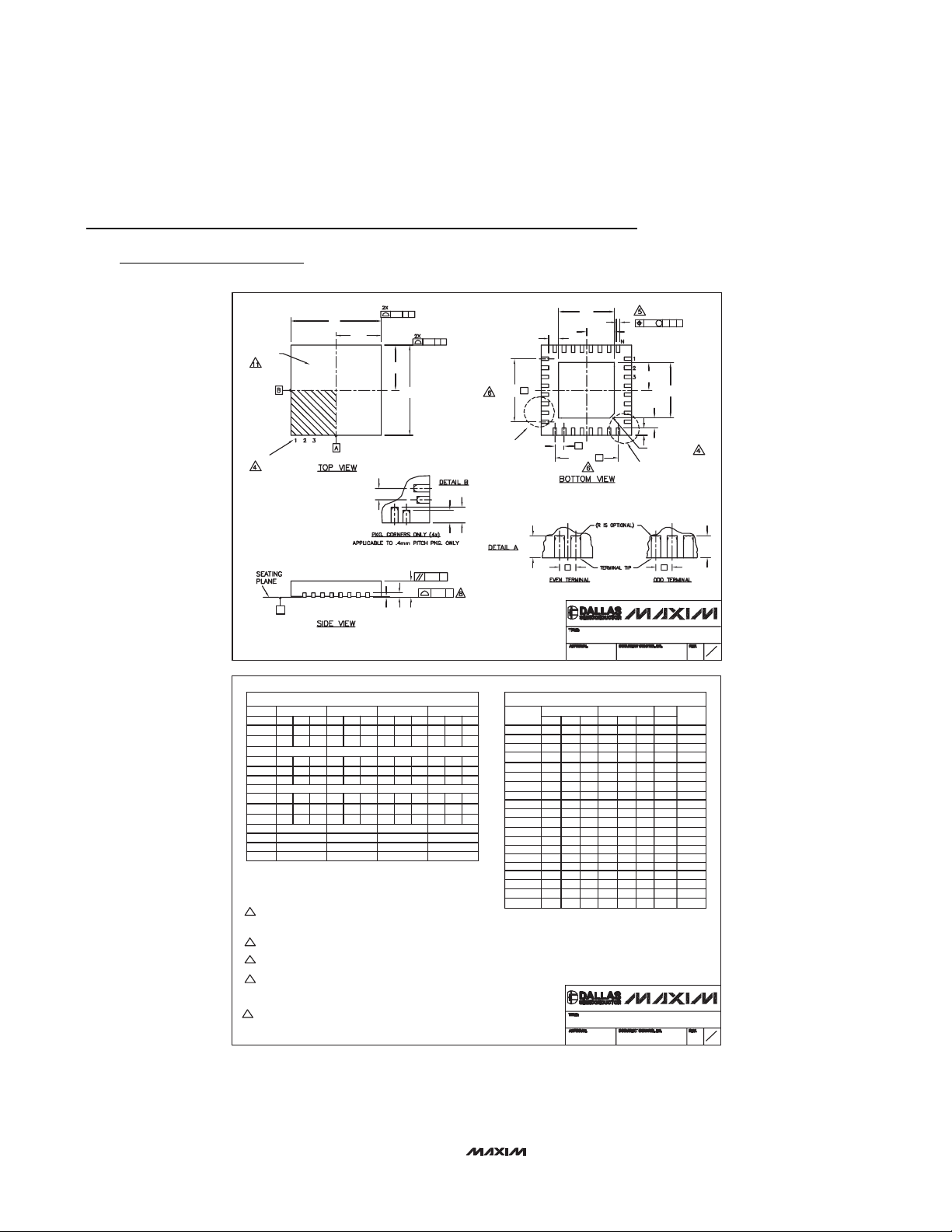
Package Information
(The package drawing(s) in this data sheet may not reflect the most current specifications. For the latest package outline information,
go to www.maxim-ic.com/packages
.)
C
XXXXX
D
0.15 C A
D/2
e
0.15
C B
E/2
E
L1
0.10 C
A
0.08 C
A3
A1
(NE-1) X e
DETAIL A
L
D2
C
L
D2/2
k
e
(ND-1) X e
L
e e
PACKAGE OUTLINE,
16, 20, 28, 32L THIN QFN, 5x5x0.8mm
b
E2/2
L
DETAIL B
21-0140
0.10 M C A B
C
E2
L
k
PIN # 1 I.D.
0.35x45∞
CC
L
F
LL
1
2
QFN THIN.EPS
MARKING
PIN # 1
I.D.
-DRAWING NOT TO SCALE-
PKG.
SYMBOL
A
A1
A3
b
D
E
e
k
L
L1
N
ND
NE
JEDEC
NOTES:
1. DIMENSIONING & TOLERANCING CONFORM TO ASME Y14.5M-1994.
2. ALL DIMENSIONS ARE IN MILLIMETERS. ANGLES ARE IN DEGREES.
3. N IS THE TOTAL NUMBER OF TERMINALS.
4. THE TERMINAL #1 IDENTIFIER AND TERMINAL NUMBERING CONVENTION SHALL
CONFORM TO JESD 95-1 SPP-012. DETAILS OF TERMINAL #1 IDENTIFIER ARE
OPTIONAL, BUT MUST BE LOCATED WITHIN THE ZONE INDICATED. THE TERMINAL #1
IDENTIFIER MAY BE EITHER A MOLD OR MARKED FEATURE.
5. DIMENSION b APPLIES TO METALLIZED TERMINAL AND IS MEASURED BETWEEN 0.25 mm AND 0.30 mm
FROM TERMINAL TIP.
6. ND AND NE REFER TO THE NUMBER OF TERMINALS ON EACH D AND E SIDE RESPECTIVELY.
7. DEPOPULATION IS POSSIBLE IN A SYMMETRICAL FASHION.
8. COPLANARITY APPLIES TO THE EXPOSED HEAT SINK SLUG AS WELL AS THE TERMINALS.
9. DRAWING CONFORMS TO JEDEC MO220, EXCEPT EXPOSED PAD DIMENSION FOR T2855-1,
T2855-3 AND T2855-6.
10. WARPAGE SHALL NOT EXCEED 0.10 mm.
11. MARKING IS FOR PACKAGE ORIENTATION REFERENCE ONLY.
12. NUMBER OF LEADS SHOWN ARE FOR REFERENCE ONLY.
-DRAWING NOT TO SCALE-
COMMON DIMENSIONS
16L 5x5
MIN. MAX.NOM.
0.70 0.800.75
0.05
0.02
0.20 REF.
0.350.30
0.25
5.10
5.00
4.90
5.105.00
4.90
0.80 BSC.
0.250--
0.30 0.500.40
---
16
4
4
WHHB
0.70
0.25
4.90
4.90
0.25
0.45
MIN.
0
---
20L 5x5
NOM.
0.75
0.02
0.20 REF.
0.30
5.00
5.00
0.65 BSC.
0.55
20
5
5
WHHC
MAX.
0.80
0.05
0.35
5.10
5.10
0.65
NOM.
0.75
0.02
0.25
5.00
5.00
0.55
28
7
7
MAX.
0.80
0.05
0.30
5.10
5.10
--
0.65
32L 5x5
NOM.
MIN.
0.75
0.70
0.02
0
0.20 REF.
0.20 0.25 0.30
5.00
4.90
5.00
4.90
0.50 BSC.
0.25
0.40
0.30
---
32
8
8
WHHD-2
MAX.
0.80
0.05
5.10
5.10
0.50
--
28L 5x5
MIN.
0.70
0
0.20 REF.
0.20
4.90
4.90
0.50 BSC.
--
0.25
0.45
---
WHHD-1
EXPOSED PAD VARIATIONS
PKG.
CODES
T1655-1
T2855-1 3.25 3.353.15 3.25
T2855-2 2.60 2.602.80 2.70 2.80
T2855-3 3.15 3.25 3.35 3.15 3.25 3.35
T2855-4 2.60 2.70 2.80 2.60 2.70 2.80
T2855-5 2.60 2.70 2.80 2.60 2.70 2.80
T2855-6 3.15 3.25 3.35 3.15 3.25 3.35
T2855-7 2.60 2.70
T3255-2
D2
MAX.
NOM.MIN.
MIN.E2NOM. MAX.
3.203.00 3.10 3.00 3.10 3.20
3.203.00T1655-2 3.10 3.00 3.10 3.20 YES
3.20
3.00T2055-2 3.10
3.103.00 3.203.103.00 3.20T2055-4
3.353.15T2055-5 3.25 3.15 3.25 3.35
3.353.15
2.70
2.80
2.60 2.70 2.80
3.35
3.15T2855-8 3.25 3.15 3.25 3.35
3.35
3.15T2855N-1 3.25 3.15 3.25 3.35
3.20
3.00
3.00 3.10 3.20
3.10
3.203.00 3.10T3255-3 3.203.00 3.10
3.203.00 3.10T3255-4 3.203.00 3.10
3.203.10T3255N-1 3.00
SEE COMMON DIMENSIONS TABLE
**
PACKAGE OUTLINE,
16, 20, 28, 32L THIN QFN, 5x5x0.8mm
21-0140
DOWN
L
BONDS
±0.15
ALLOWED
NO
**
**
NO3.203.103.003.10T1655N-1 3.00 3.20
**
3.203.00 3.10
3.203.103.00
NO
**
YES3.103.00 3.203.103.00 3.20T2055-3
**
NO
**
Y
0.40
NO
**
NO
**
YES
**
YES
**
NO
**
NO
**
YES
**
Y
0.40
N
**
NO
**
YES
**
NO
**
NO
**
2
F
2
 Loading...