

Page 1
General Description
The MAX9486 low-cost, high-performance clock synthesizer with an 8kHz input reference clock provides six
buffered LVTTL clock outputs at 35.328MHz. The clock
synthesizer can be used to generate the clocks for T1,
E1, T3, E3, and xDSL.
The MAX9486 has two phase-lock loops (PLLs). The
first PLL uses a voltage-controlled crystal oscillator
(VCXO). The second PLL is a frequency multiplier. With
the two PLLs, the MAX9486 generates the output frequency at 35.328MHz. In addition, this device generates a jitter-suppressed 8kHz output that provides a
better source for the reference clock relay.
The MAX9486 is available in a 24-pin TSSOP package
and operates over the extended operating temperature
range of -40°C to +85°C and a single +3V to +3.6V
power-supply range.
Applications
Telecom Equipment Using T1, E1, T3, E3, and
ISDN Protocols
xDSL Equipment in CO with Interface to the
Telecom Protocols
Features
♦ 8kHz Input Reference CLK
♦ High-Jitter Rejection on the Reference CLK
♦ Synthesizer Locks to the 8kHz Reference with a
±200ppm Range
♦ Output Frequency: 35.328MHz
♦ Six Buffered LVTTL Low-Jitter Outputs
♦ One 8kHz Reference CLK Relay Output
♦ +3.3V Supply Operation
♦ 24-Pin TSSOP Package
MAX9486
8kHz Reference Clock Synthesizer
with Multiple Outputs at 35.328MHz
________________________________________________________________ Maxim Integrated Products 1
Ordering Information
19-3345; Rev 0; 8/04
For pricing, delivery, and ordering information, please contact Maxim/Dallas Direct! at
1-888-629-4642, or visit Maxim’s website at www.maxim-ic.com.
EVALUATION KIT
AVAILABLE
PART TEMP RANGE PIN-PACKAGE
MAX9486EUG -40°C to +85°C 24 TSSOP
24
23
22
21
20
19
18
17
1
2
3
4
5
6
7
8
CLK1
GND
CLK2
V
DD
V
DDP
REIN
REO
TOP VIEW
CLK3
V
DD
GND
CLK4X2
V
DD
X1
GNDP
16
15
14
13
9
10
11
12
V
DD
CLK5
GND
CLK6SETI
LP1
LP2
GND
TSSOP
MAX9486
SHDN
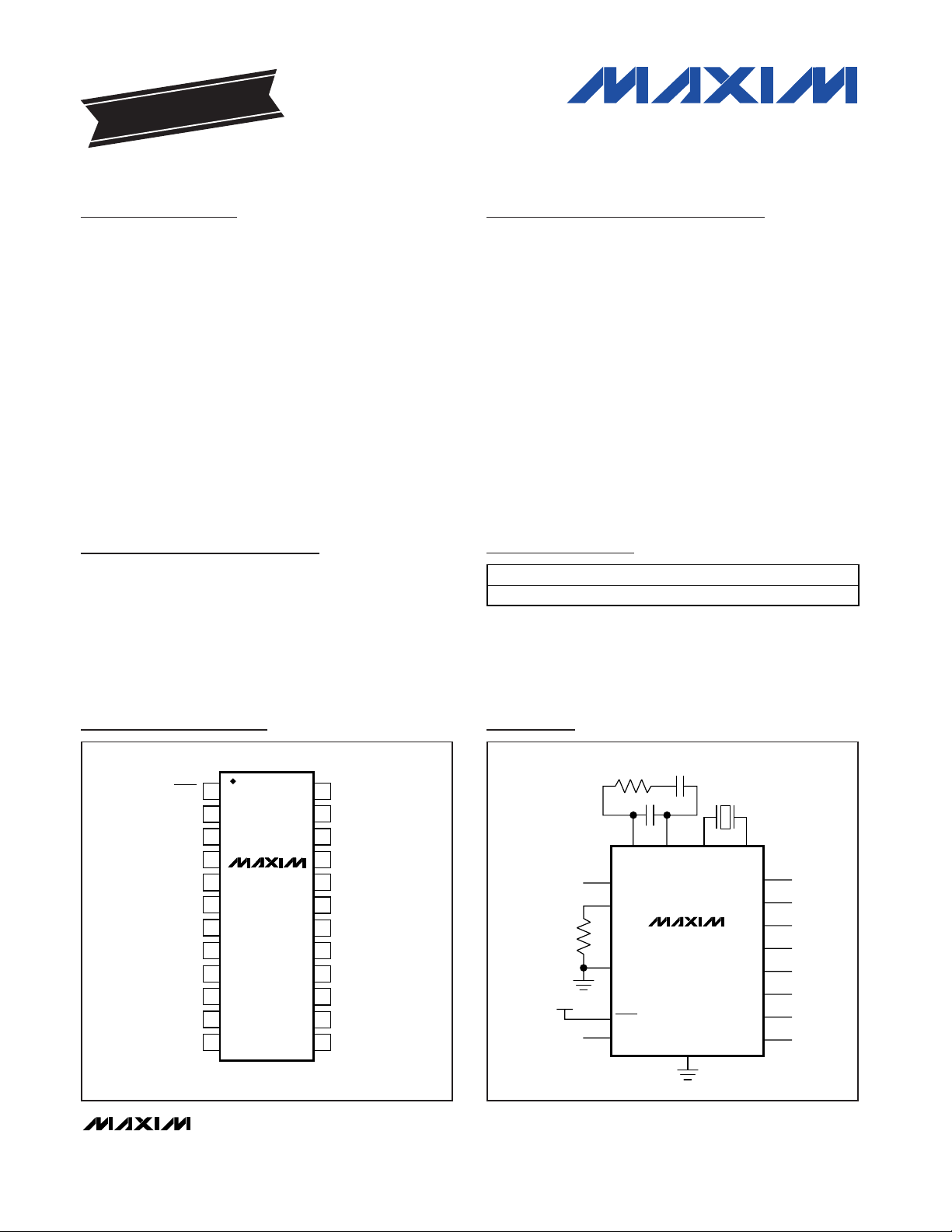
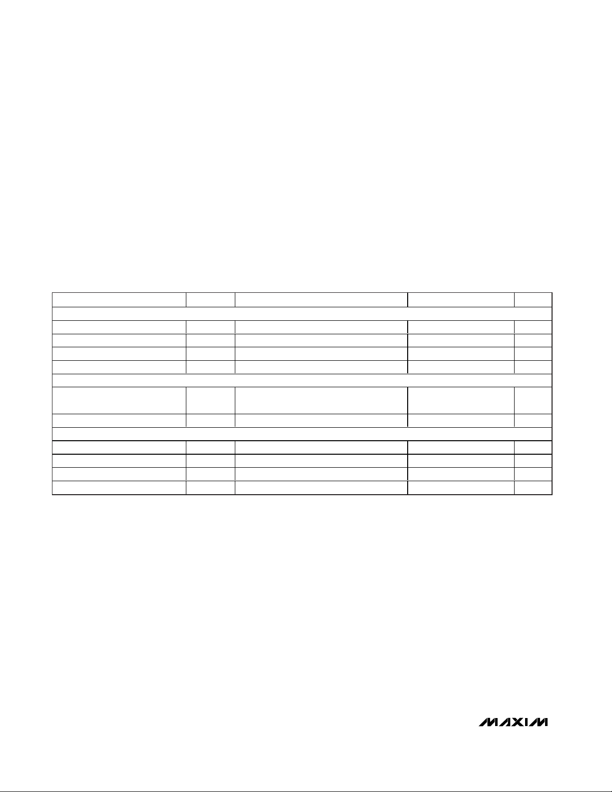
Pin Configuration
MAX9486
CLK2
X1
CLK1
V
DDP
GNDP
X2
REO
CLK6
CLK5
CLK4
CLK3
GND
V
DD
LP1 LP2
REIN
R
SET
R
1
C
1
C
2
SETI
V
DD
SHDN
Typical Application Circuit
Page 2
MAX9486
8kHz Reference Clock Synthesizer
with Multiple Outputs at 35.328MHz
2 _______________________________________________________________________________________
ABSOLUTE MAXIMUM RATINGS
DC ELECTRICAL CHARACTERISTICS
(VDD= V
DDP
= +3.0V to +3.6V, TA= -40°C to +85°C, unless otherwise noted. Typical values are at VDD= V
DDP
= +3.3V, TA=
+25°C.) (Note 1)
Stresses beyond those listed under “Absolute Maximum Ratings” may cause permanent damage to the device. These are stress ratings only, and functional
operation of the device at these or any other conditions beyond those indicated in the operational sections of the specifications is not implied. Exposure to
absolute maximum rating conditions for extended periods may affect device reliability.
VDDto GND...........................................................-0.3V to +4.0V
V
DDP
to GNDP.......................................................-0.3V to +4.0V
SHDN, REO, REIN, X1, X2, CLK_ to GND ...-0.3V to (VDD+ 0.3V)
LP1, SETI to GNDP.....................................-0.3V to (V
DD
+ 0.3V)
LP2 Internally Connected to GNDP
Short-Circuit Duration of Outputs ...............................Continuous
Continuous Power Dissipation (T
A
= +70°C)
24-Pin TSSOP (derate 12.2mW/°C above +70°C) .......976mW
Operating Temperature Range ...........................-40°C to +85°C
Maximum Junction Temperature .....................................+150°C
Storage Temperature Range .............................-60°C to +150°C
ESD Rating (Human Body Model) .......................................±2kV
Lead Temperature (soldering, 10s) .................................+300°C
PARAMETER
CONDITIONS
UNITS
DIGITAL INPUTS (REIN,
SHDN
)
Input High Logic Level V
IH
2.0 V
Input Low Logic Level V
IL
0.8 V
Input-Current High Level I
IH
VIN = V
DD
20 µA
Input-Current Low Level I
IL
VIN = 0 -20 µA
DIGITAL OUTPUT CLOCKS (CLK1–CLK6, REO)
Output High Logic Level V
OH
IOH = -4mA
V
Output Low Logic Level V
OL
IOL = 4mA 0.4 V
POWER SUPPLY (VDD, V
DDP
)
Power-Supply Range V
DD
3.0 3.6 V
PLL Power-Supply Range V
DDP
3.0 3.6 V
Power-Supply Current
(Note 2) 13 25 mA
Shutdown Supply Current I
SHDN
830µA
SYMBOL
MIN TYP MAX
VDD -
0.6V
IDD + I
DDP
Page 3
MAX9486
8kHz Reference Clock Synthesizer
with Multiple Outputs at 35.328MHz
_______________________________________________________________________________________ 3
Note 1: Specifications are 100% tested at TA= +25°C. Specifications over temperature are guaranteed by design and characterization.
Note 2: No load on clock outputs.
Note 3: Guaranteed by design.
Note 4: Crystal loading capacitance is 14pF.
AC ELECTRICAL CHARACTERISTICS
(VDD= V
DDP
= +3.0V to +3.6V, CL= 20pF, TA= -40°C to +85°C, unless otherwise noted. Typical values are at VDD= V
DDP
= +3.3V,
T
A
= +25°C.) (Note 3)
PARAMETER
CONDITIONS
UNITS
DIGITAL OUTPUT CLOCKS (CLK1–CLK6)
Frequency Range f
OUT
MHz
Clock Rise Time T
R1
20% to 80% V
DD
1.8 ns
Clock Fall Time T
F1
80% to 20% V
DD
1.8 ns
Duty Cycle 40 50 60 %
Period Jitter J
PP1
Peak-to-peak
ps
Output Skew t
S
Peak-to-peak
ps
REFERENCE CLOCK OUTPUT (REO)
Frequency f
REF
8 kHz
Clock Rise Time T
R2
1.8 ns
Clock Fall Time T
F2
1.8 ns
Duty Cycle 40 50 60 %
VCXO
Crystal Frequency f
XTL
MHz
Crystal Accuracy
Including frequency accuracy and
temperature range
ppm
VCXO Pulling Range (Note 4)
ppm
Input Reference CLK Pulse Width
t
W
Measured at high or low states 10 ns
SYMBOL
MIN TYP MAX
35.328
120
185
17.664
±25
-200 +200
Page 4

MAX9486
8kHz Reference Clock Synthesizer
with Multiple Outputs at 35.328MHz
4 _______________________________________________________________________________________
Typical Operating Characteristics
(VDD= V
DDP
= +3.3V, TA= +25°C, unless otherwise noted.)
OUTPUT WAVEFORM
MAX9486 toc01
10ns/div
OUTPUT CLOCK JITTER (
P-P
)
vs. TEMPERATURE
MAX9486 toc02
TEMPERATURE (°C)
OUTPUT CLOCK JITTER (ps)
603510-15
80
90
100
110
120
130
140
-40 85
OUTPUT CLOCK JITTER (
P-P
)
vs. SUPPLY VOLTAGE
MAX9486 toc03
SUPPLY VOLTAGE (V)
OUTPUT CLOCK JITTER (ps)
3.53.43.33.23.1
100
105
110
115
120
125
130
135
140
3.0 3.6
OUTPUT FREQUENCY VARIATION
vs. INPUT REFERENCE FREQUENCY
MAX9486 toc04
INPUT REFERENCE FREQUENCY (kHz)
OUTPUT FREQUENCY VARIATION (ppm)
8.0028.0018.0007.9997.998
0
50
-50
100
-100
150
-150
200
-200
250
-250
CENTERED AT
35.328MHz
SUPPLY CURRENT (IDD + I
DDP
)
vs. SUPPLY VOLTAGE
MAX9486 toc05
SUPPLY VOLTAGE (V)
SUPPLY CURRENT (mA)
3.53.43.33.23.1
10
12
14
16
8
3.0 3.6
TA = -40°C
TA = +25°C
TA = +85°C
SHUTDOWN SUPPLY CURRENT
vs. SUPPLY VOLTAGE
MAX9486 toc06
SUPPLY VOLTAGE (V)
SUPPLY CURRENT (µA)
3.53.43.33.23.1
8
9
10
11
12
7
6
3.0 3.6
TA = +85°C
TA = -40°C
TA = +25°C
Page 5

MAX9486
8kHz Reference Clock Synthesizer
with Multiple Outputs at 35.328MHz
_______________________________________________________________________________________ 5
PIN
FUNCTION
1 SHDN Active-Low Shutdown Input
2 REO Reference Clock Output. REO is an 8kHz reference clock output with jitter suppression.
3 REIN Reference Input
4V
DDP
Phase-Lock Loop (PLL) Power Supply. Bypass V
DDP
with 0.1µF and 0.001µF capacitors to GNDP.
5 GNDP PLL Ground
6X1Crystal Input 1. Connect X1 to a fundamental mode crystal for the VCXO.
7, 16, 19,
21
V
DD
Digital Power Supply. Bypass VDD with 0.1µF and 0.001µF capacitors to GND.
8X2Crystal Input 2. Connect X2 to a fundamental mode crystal for the VCXO.
9, 14, 18,
23
GND Ground
10 LP2
External Filter 2. Connect the loop filter capacitors and a resistor between LP1 and LP2 (see the Typical
Application Circuit). LP2 is internally connected to GNDP.
11 LP1
External Filter 1. Connect the loop filter capacitors and a resistor between LP1 and LP2 (see the Typical
Application Circuit).
12 SETI
Charge-Pump Current-Setting Input. Connect a resistor from SETI to GNDP to set PLL charge-pump current
(see the Detailed Description section).
13 CLK6 Clock Output 6 at 35.328MHz
15 CLK5 Clock Output 5 at 35.328MHz
17 CLK4 Clock Output 4 at 35.328MHz
20 CLK3 Clock Output 3 at 35.328MHz
22 CLK2 Clock Output 2 at 35.328MHz
24 CLK1 Clock Output 1 at 35.328MHz
Pin Description
NAME
Page 6

MAX9486
Detailed Description
The MAX9486 is a high-performance clock synthesizer
with an 8kHz input reference clock. This device generates six identical buffered LVTTL clock outputs at
35.328MHz. The MAX9486 features two PLLs. The first
PLL (PLL1) uses an internal VCXO, locked to the 8kHz
reference CLK, to generate a 17.664MHz CLK output
for the second PLL (PLL2). PLL2 multiplies the VCXO
frequency by a factor of 2 to produce the 35.328MHz
outputs. In addition, this device features a low-jitter
8kHz output that provides a better source for the reference clock relay (see the Functional Diagram).
Power-Up
At power-up, all the outputs are disabled and pulled
low (to GND) for at least 256ms. After 256ms, the crystal oscillator starts oscillation. The input reference clock
for PLL1 is 8kHz and its output frequency, 17.664MHz,
is also the reference clock for PLL2. If the 8kHz reference clock is not present at power-up, the output frequency of PLL1 is locked to the center frequency of the
crystal oscillator.
8kHz Reference CLK Monitor
The MAX9486 features an internal clock (CLK) monitor
circuitry to detect the presence of the external 8kHz reference clock. The internal CLK monitor continuously
monitors the number of low-to-high transitions within a
three-cycle (at 8kHz) time window. If the transition number is less than two, the internal CLK monitor states
loss of the reference CLK. However, if in a three-cycle
time window the monitor counts two or three transitions,
it considers the input reference clock as present. When
the monitor detects the absence of the 8kHz reference
clock, PLL2 is forced to lock to the crystal oscillator frequency. However, when the monitor detects the return
of the reference clock, PLL1 locks to the reference
clock again.
Clock Outputs (CLK1 to CLK6) and REO
The MAX9486 uses a 17.664MHz crystal and a reference clock (REIN) to generate six identical outputs,
CLK1 to CLK6, at 35.328MHz. All CLK_ outputs are
LVTTL with a skew of 185ps. The MAX9486 also regenerates the 8kHz reference CLK at REO output.
Voltage-Controlled Crystal
Oscillator (VCXO)
The MAX9486’s internal VCXO takes an external
17.664MHz crystal as the base frequency and has a
pulling range of approximately ±200ppm. This configuration also makes the VCXO PLL become a narrowband
filter to reject high-frequency jitter on the input reference
and eliminate it from the REO and CLK_ outputs.
8kHz Reference Clock Synthesizer
with Multiple Outputs at 35.328MHz
6 _______________________________________________________________________________________
MAX9486
PLL1
CLK2
VCXO
X1
CLK1
V
DDP GNDP
/2208
PHASE DETECTOR
AND
CHARGE PUMP
PLL2
VCO
/2
X2
REO
CLK6
CLK5
CLK4
CLK3
GND
V
DD
LP1 LP2
REFERENCE CLK
MONITOR
REIN
SETI
PHASE DETECTOR,
CHARGE PUMP, AND
LOOP FILTER
SHDN
Functional Diagram
Page 7

SHDN
Mode
The MAX9486 features a shutdown mode with a supply
current less than 8µA (typ). Drive SHDN low to get the
device into shutdown mode. In this mode, all the outputs go low and both PLLs are powered down. After
SHDN goes high, the outputs still stay low for an additional 256ms to allow both PLLs to be stabilized before
the outputs are enabled again.
Applications Information
Crystal Selection
The MAX9486 uses a 17.664MHz crystal as the base
frequency for the VCXO. It is important to use a correct
type of quartz crystal to avoid reducing frequency
pulling range, or excessive output phase jitter.
Choose an AT-cut crystal that oscillates at 17.664MHz
on its fundamental mode with a variation of ±25ppm
including frequency accuracy and operating temperature range. The crystal’s load capacitance should be
14pF. Pulling range may vary depending on the crystal
used. Refer to the MAX9486 evaluation kit for details.
PLL1 Loop Filter
The MAX9486 features two PLLs: PLL1 and PLL2. The
first phased-lock loop, PLL1, contains an integrated
VCXO that uses an external crystal to track the input
reference signal and attenuate input jitter. Figure 1
shows the external loop filter of the PLL containing
resistor R1 and two capacitors, C1 and C2. This loop
filter is connected between LP1 and LP2 as shown in
the Typical Operating Circuit. The loop-filter bandwidth
is determined by C1, C2, R1, and R
SET
where R
SET
is
used to set the value of the charge-pump current. The
typical values of C1, C2, R1, and R
SET
are 22nF,
560pF, 1000kΩ, and 13kΩ, respectively.
Use the following equation to calculate a PLL loop
bandwidth in Hz:
BW = (R1 x I
SETI
x 940) / N
where R1 (Ω) is the resistor in the PLL1 loop filter
(Figure 1), I
SETI
(A) is the charge-pump current calcu-
lated from the equation in the Charge-Pump Current
Setting section, and N is the crystal PLL frequency
divider equal to 2208.
The loop-damping factor is calculated by:
where C1 (F) and R1 (Ω) are the values of the capacitor
and the resistor in the PLL1 loop filter shown in
Figure 1; I
SETI
is calculated as shown in the Charge-
Pump Current Setting section and N = 2208.
The following equation shows the relationship between
components C1 and C2 in the loop filter:
C2 ≤ C1/20
Charge-Pump Current Setting
The MAX9486 also allows external setting of the chargepump current in PLL1. Connect a resistor from SETI to
GNDP to set the PLL1 charge-pump current:
Charge-Pump Current = 2.4 x 1000 / (R
SET
(kΩ) + 1)
where R
SET
is in kΩ and the value of the charge-pump
current is in µA.
The loop response can be adjusted to meet individual
application requirements since the charge-pump current and all the filter components for the VCXO loop
can be set externally.
Board Layout and Bypassing
The MAX9486’s high-oscillator frequency makes proper
layout important to ensure stability. For best performance,
place components as close as possible to the device.
Digital or AC transient signals on GND can create noise
at the clock outputs. Return GND to the highest quality
ground available. Bypass VDDand V
DDP
with 0.1µF
and 0.001µF capacitors, placed as close to the device
as possible. Careful PC board ground layout minimizes
crosstalk between the outputs and digital inputs.
Traces must be as short as possible on LP1 and LP2
and connect the capacitors and the resistor as close as
possible to the device.
Chip Information
TRANSISTOR COUNT: 7512
PROCESS: CMOS
DampingFactor
RIC
N
SETI
=×
××
11
2
5900
MAX9486
8kHz Reference Clock Synthesizer
with Multiple Outputs at 35.328MHz
_______________________________________________________________________________________ 7
R1
C1
C2
LP1
LP2
Figure 1. Typical Loop Filter
Page 8

MAX9486
8kHz Reference Clock Synthesizer
with Multiple Outputs at 35.328MHz
Maxim cannot assume responsibility for use of any circuitry other than circuitry entirely embodied in a Maxim product. No circuit patent licenses are
implied. Maxim reserves the right to change the circuitry and specifications without notice at any time.
8 _____________________Maxim Integrated Products, 120 San Gabriel Drive, Sunnyvale, CA 94086 408-737-7600
© 2004 Maxim Integrated Products Printed USA is a registered trademark of Maxim Integrated Products.
Package Information
(The package drawing(s) in this data sheet may not reflect the most current specifications. For the latest package outline information,
go to www.maxim-ic.com/packages
.)
TSSOP4.40mm.EPS
 Loading...