

Page 1
19-0547; Rev 0; 5/06
High-Precision Clock Generators
with Integrated VCXO
General Description
The MAX9450/MAX9451/MAX9452 clock generators
provide high-precision clocks for timing in SONET/SDH
systems or Gigabit Ethernet systems. The MAX9450/
MAX9451/MAX9452 can also provide clocks for the highspeed and high-resolution ADCs and DACs in 3G base
stations. Additionally, the devices can also be used as a
jitter attenuator for generating high-precision CLK signals.
The MAX9450/MAX9451/MAX9452 feature an integrated
VCXO. This configuration eliminates the use of an external VCXO and provides a cost-effective solution for generating high-precision clocks. The MAX9450/MAX9451/
MAX9452 feature two differential inputs and clock outputs. The inputs accept LVPECL, LVDS, differential signals, and LVCMOS. The input reference clocks range
from 8kHz to 500MHz.
The MAX9450/MAX9451/MAX9452 offer LVPECL, HSTL,
and LVDS outputs, respectively. The output range is up
to 160MHz, depending on the selection of crystal. The
input and output frequency selection is implemented
through the I2C* or SPI™ interface. The MAX9450/
MAX9451/MAX9452 feature clock output jitter less than
0.8ps RMS (in a 12kHz to 20MHz band) and phasenoise attenuation greater than -130dBc/Hz at 100kHz.
The phase-locked loop (PLL) filter can be set externally,
and the filter bandwidth can vary from 1Hz to 20kHz.
The MAX9450/MAX9451/MAX9452 feature an input
clock monitor with a hitless switch. When a failure is
detected at the selected reference clock, the device
can switch to the other reference clock. The reaction to
the recovery of the failed reference clock can be
revertive or nonrevertive. If both reference clocks fail,
the PLL retains its nominal frequency within a range of
±20ppm at +25°C.
The MAX9450/MAX9451/MAX9452 operate from a 2.4V to
3.6V supply and are available in 32-pin TQFP packages
with exposed pads.
Applications
SONET/SDH Systems
10 Gigabit Network Routers and Switches
3G Cellular Phone Base Stations
General Jitter Attenuation
*Purchase of I2C components from Maxim Integrated Products,
Inc., or one of its sublicensed Associated Companies, conveys
a license under the Philips I
ponents in an I
2
C Standard Specification as defined by Philips.
the I
SPI is a trademark of Motorola, Inc.
2
C system, provided that the system conforms to
2
C Patent Rights to use these com-
Features
♦ Integrated VCXO Provides a Cost-Effective
Solution for High-Precision Clocks
♦ 8kHz to 500MHz Input Frequency Range
♦ 15MHz to 160MHz Output Frequency Range
♦ I2C or SPI Programming for the Input and Output
Frequency Selection
♦ PLL Lock Range > ±60ppm
♦ Two Differential Outputs with Three Types of
Signaling: LVPECL, LVDS, or HSTL
♦ Input Clock Monitor with Hitless Switch
♦ Internal Holdover Function within ±20ppm of the
Nominal Frequency
♦ Low Output CLK Jitter: < 0.8ps RMS in the 12kHz
to 20MHz Band
♦ Low Phase Noise > -130dBc at 100kHz
Ordering Information
PART PIN-PACKAGE OUTPUT PKG CODE
MAX9450EHJ+ 32 TQFP-EP** LVPECL H32E-6
MAX9451EHJ+† 32 TQFP-EP** HSTL H32E-6
MAX9452EHJ+† 32 TQFP-EP** LVDS H32E-6
Note: All devices are specified over the -40°C to +85°C
temperature range.
+Denotes lead-free package.
**EP = Exposed pad.
†Future product—contact factory for availability.
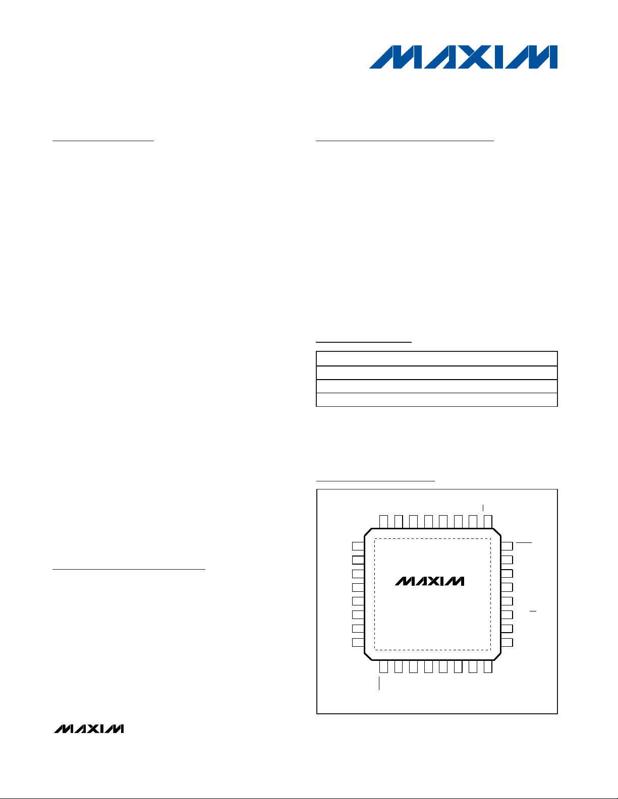
Pin Configuration
TOP VIEW
DD
X1
X2
V
DDA
LP1
LP2
GNDA
25V
26
27
28
29
30
31
32RJ
DDQ
CLK1+
CLK1-
MAX9450
MAX9451
MAX9452
EXPOSED PAD
SEL0
SEL1
GND
212223
(GND)
IN0+
TQFP
V
24 20
+
2
1
LOCK
(5mm x 5mm)
5
CLK0+
IN0-
19
6
CLK0-
DD
V
DDQ
V
OE
18
17
16
CMON
AD1
15
AD0
14
SDA
13
SCL
12
GND/CS
11
MR
10
INT
9
7
834
IN1-
IN1+
MAX9450/MAX9451/MAX9452
________________________________________________________________ Maxim Integrated Products 1
For pricing, delivery, and ordering information, please contact Maxim/Dallas Direct! at
1-888-629-4642, or visit Maxim’s website at www.maxim-ic.com.
Page 2
MAX9450/MAX9451/MAX9452
High-Precision Clock Generators
with Integrated VCXO
2 _______________________________________________________________________________________
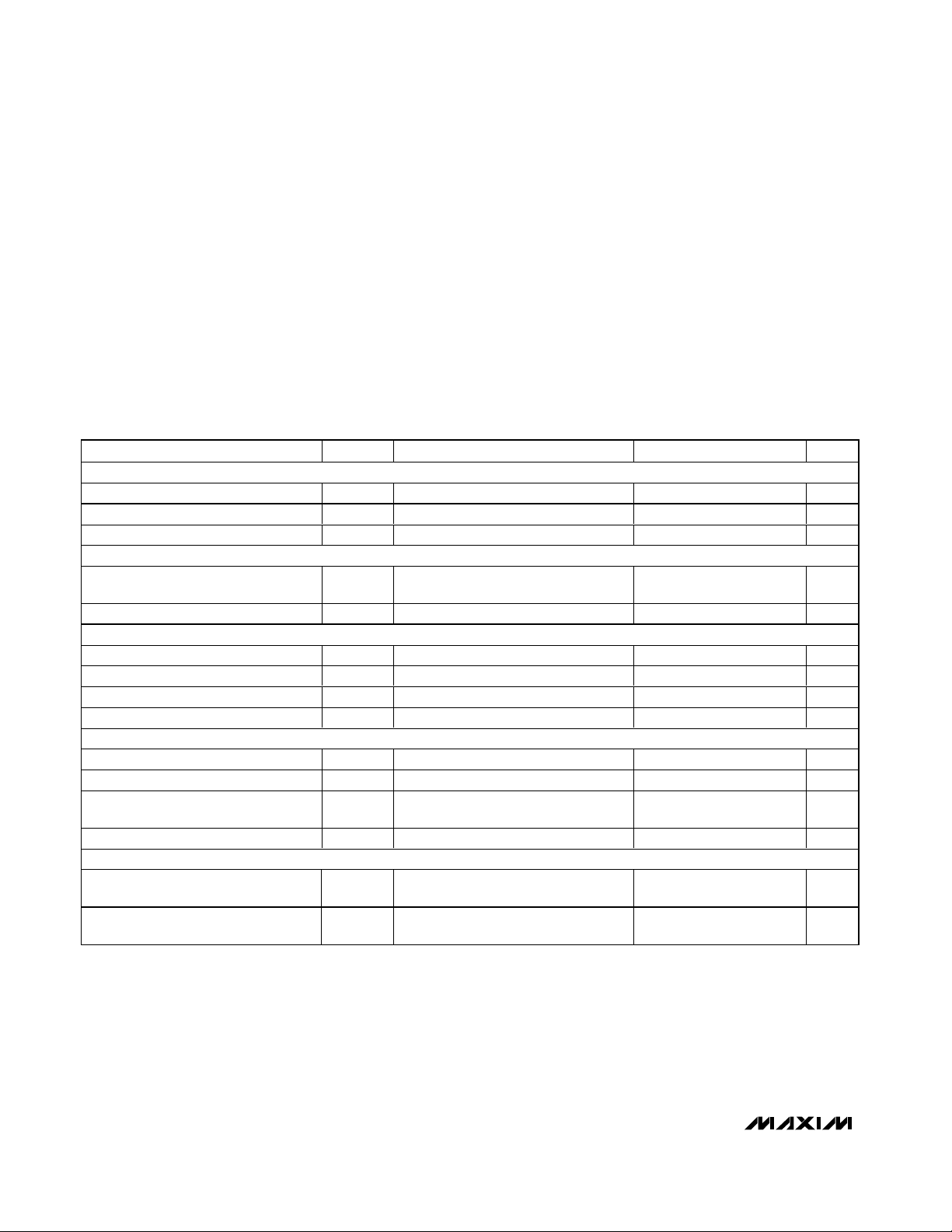
ABSOLUTE MAXIMUM RATINGS
DC ELECTRICAL CHARACTERISTICS
(V
DDA
= VDD= V
DDQ
= 2.4V to 3.6V, and V
DDQ
= 1.4V to 1.6V for MAX9451, TA= -40°C to +85°C. Typical values at V
DDA
= VDD=
V
DDQ
= 3.3V, and V
DDQ
= 1.5V for MAX9451, TA= +25°C, unless otherwise noted.)
Stresses beyond those listed under “Absolute Maximum Ratings” may cause permanent damage to the device. These are stress ratings only, and functional
operation of the device at these or any other conditions beyond those indicated in the operational sections of the specifications is not implied. Exposure to
absolute maximum rating conditions for extended periods may affect device reliability.
VDDto GND...........................................................-0.3V to +4.0V
V
DDA
to GNDA ......................................................-0.3V to +4.0V
All Other Pins to GND ...................................-0.3V to V
DD
+ 0.3V
Short-Circuit Duration (all pins) ..................................Continuous
Continuous Power Dissipation (T
A
= +85°C)
32-Pin TQFP (derate 27.8mW/°C above +70°C)........2222mW
Storage Temperature Range .............................-65°C to +165°C
Maximum Junction Temperature .....................................+150°C
Operating Temperature Range ...........................-40°C to +85°C
Lead Temperature (soldering, 10s) .................................+300°C
ESD Protection
Human Body Model (R
D
= 1.5kΩ, CS= 100pF) ..............±2kV
PARAMETER
CONDITIONS
UNITS
LVCMOS INPUT (SEL_, CMON, OE, MR)
Input High Level V
IH1
2.0
V
Input Low Level V
IL1
0 0.8 V
Input Current I
IN1
VIN = 0V to V
DD
-50 +50 µA
LVCMOS OUTPUT (INT, LOCK)
Output High Level V
OH1IOH1
= -4mA
V
Output Low Level V
OL1IOL1
= 4mA 0.4 V
THREE-LEVEL INPUT (AD0, AD1)
Input High Level V
IH2
1.8 V
Input Low Level V
IL2
0.8 V
Input Open Level V
IO2
Measured at the opened inputs
V
Input Current
V
IL2
= 0V or V
IH2
= V
DD
-15 +15 µA
DIFFERENTIAL INPUTS (IN0, IN1)
Differential Input High Threshold V
IDH
V
ID
= V
IN+
- V
IN-
50 mV
Differential Input Low Threshold V
IDL
V
ID
= V
IN+
- V
IN-
-50 mV
Common-Mode Input-Voltage Range V
COM
V
ID
= V
IN+ - VIN-
2.4
V
Input Current
-1 +1 µA
MAX9450 OUTPUTS (CLK0, CLK1) (LVPECL)
Output High Voltage V
OH2
50Ω load connected to V
DDQ
- 2.0V
V
Output Low Voltage V
OL2
50Ω load connected to V
DDQ
- 2.0V
V
SYMBOL
MIN TYP MAX
V
DD
V
DD
- 0.4
I
IL2, IIH2
I
IN+, IIN-
1.05 1.35
|V
/ 2|
ID
V
D D Q
- |V
- 1.42
V
D D Q
- 2.15
ID
V
D D Q
- 1.00
V
D D Q
- 2.15
/ 2|
Page 3
MAX9450/MAX9451/MAX9452
High-Precision Clock Generators
with Integrated VCXO
_______________________________________________________________________________________ 3
DC ELECTRICAL CHARACTERISTICS (continued)
(V
DDA
= VDD= V
DDQ
= 2.4V to 3.6V, and V
DDQ
= 1.4V to 1.6V for MAX9451, TA= -40°C to +85°C. Typical values at V
DDA
= VDD=
V
DDQ
= 3.3V, and V
DDQ
= 1.5V for MAX9451, TA= +25°C, unless otherwise noted.)
PARAMETER
SYMBOL
CONDITIONS
MIN
TYP
MAX
UNITS
SERIAL INTERFACE INPUT, OUTPUT (SCL, SDA, CS)
Input High Level V
IH
V
Input Low Level V
IL
V
Input Leakage Current I
IL
±1 µA
Output Low Level V
OL
3mA sink current 0.4 V
Input Capacitance C
I
10 pF
POWER CONSUMPTION
VDD and V
DDA
Supply Current I
CC1
Output clock frequency = 155MHz 55 85 mA
V
DDQ
Supply Current I
CC2
Output clock frequency = 155MHz
(MAX9450)
55 80 mA
AC ELECTRICAL CHARACTERISTICS
(V
DDA
= VDD= V
DDQ
= 2.4V to 3.6V, and V
DDQ
= 1.4V to 1.6V for MAX9451, TA= -40°C to +85°C. |VID| = 200mV, V
COM
= |VID/ 2| to
2.4 - |V
ID
/ 2|. Typical values at V
DDA
= VDD= V
DDQ
= 3.3V and V
DDQ
= 1.5V for MAX9451, TA= +25°C. CL= 10pF, clock output =
155.5MHz and clock input = 19.44MHz, unless otherwise noted.) (Note 1)
PARAMETER
CONDITIONS
UNITS
CLK OUTPUTS (CLK0, CLK1)
Reference Input Frequency f
IN
Measured at IN0 or IN1
500
MHz
Output Frequency f
OUT
Measured at CLK0 or CLK1 15 160
MHz
VCXO Pulling Range CL = 8pF (Note 2) ±50
ppm
Output-to-Output Skew t
SKO
Skew between CLK0 and CLK1 90 ps
Rise Time t
R
20% to 80% of output swing 0.4
ns
Fall Time t
F
80% to 20% of output swing 0.4
ns
Duty Cycle 44 56 %
Period Jitter (RMS) T
J
0.8 ps
1kHz offset -70
dBc/Hz
10kHz offset
dBc/Hz
Phase Noise
100kHz offset
dBc/Hz
SYMBOL
0.7
x V
DD
0.3
x V
MIN TYP MAX
DD
0.008
Measured at the band 12kHz to 20MHz
-110
-130
0.585
0.585
Page 4
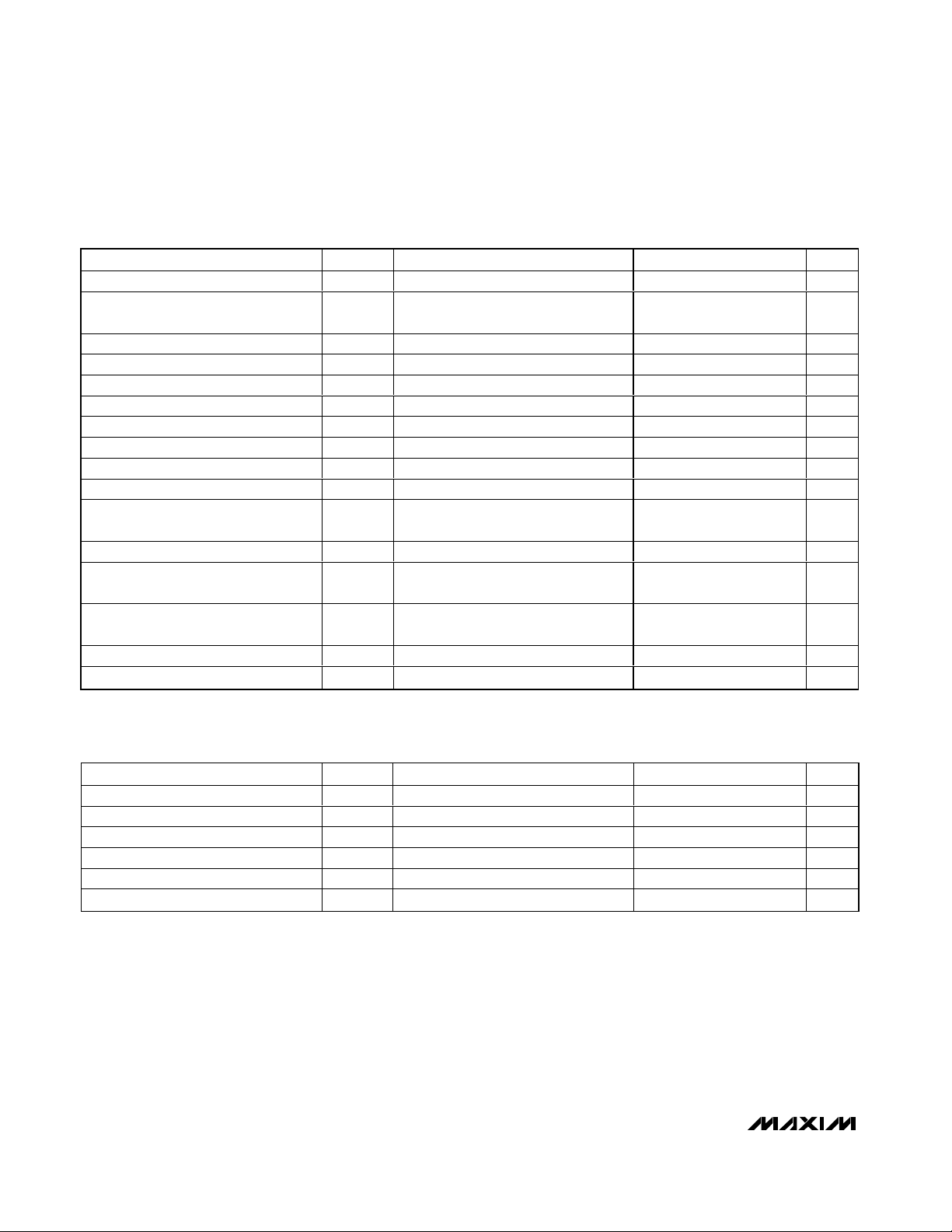
Note 1: All timing AC electrical characteristics and timing specifications are guaranteed by design and not production tested.
Note 2: The VCXO tracks the input clock frequency by ±50ppm.
Note 3: A master device must provide a hold time of at least 300ns for the SDA signal to bridge the undefined regions of SCL’s
falling edge.
Note 4: C
B
= total capacitance of one bus line in pF. Tested with CB= 400pF.
Note 5: Input filters on SDA and SCL suppress noise spikes less than 50ns.
PARAMETER
CONDITIONS
UNITS
Serial-Clock Frequency f
SCL
2
MHz
CS Fall to CLK Rise Setup Time t
CSS
ns
DIN Setup Time t
DS
ns
DIN Hold Time t
DH
0ns
CLK High to CS High t
CSH
0ns
CS Pulse-High Time t
CSW
20 ns
SERIAL SPI INTERFACE TIMING CHARACTERISTICS
(VDD= 2.4V to 3.6V, TA= -40°C to +85°C. See Figure 7 for the timing parameters definition.)
MAX9450/MAX9451/MAX9452
High-Precision Clock Generators
with Integrated VCXO
4 _______________________________________________________________________________________
PARAMETER
CONDITIONS
UNITS
Serial Clock f
SCL
400
kHz
Bus Free Time Between STOP and
START Conditions
t
BUF
1.3 µs
Rep eated H ol d Ti m e S TART C ond i ti on
0.6 µs
0.6 µs
STOP Condition Setup Time
0.6 µs
Data Hold Time
(Note 3) 100 ns
Data Setup Time
100 ns
SCL Clock-Low Period t
LOW
1.3 µs
SCL Clock-High Period t
HIGH
0.7 µs
t
R
300 ns
t
R
(Note 4)
20
ns
t
F
300 ns
Minimum Receive SCL/SDA Fall Time t
F
(Note 4)
20
ns
Fall Time of SDA, Transmitting t
F,TX
(Note 4)
20
250 ns
Pulse Width of Suppressed Spike t
SP
(Note 5) 0 50 ns
Capacitive Load for Each Bus Line C
B
(Note 4) 400 pF
SERIAL I2C-COMPATIBLE INTERFACE TIMING CHARACTERISTICS
(VDD= 2.4V to 3.6V, TA= -40°C to +85°C. See Figure 4 for the timing parameters definition.)
Rep eated S TART C ond i ti on S etup Ti m et
Maximum Receive SCL/SDA Rise Time
SYMBOL
t
HD,STA
SU,STA
t
SU,STO
t
HD,DAT
t
SU,DAT
MIN TYP MAX
Minimum Receive SCL/SDA Rise Time
Maximum Receive SCL/SDA Fall Time
SYMBOL
+ 0.1 x C
b
+ 0.1 x C
b
+ 0.1C
b
MIN TYP MAX
12.5
12.5
Page 5
MAX9450/MAX9451/MAX9452
High-Precision Clock Generators
with Integrated VCXO
_______________________________________________________________________________________ 5
VDD AND V
DDA
SUPPLY CURRENT
vs. VOLTAGE
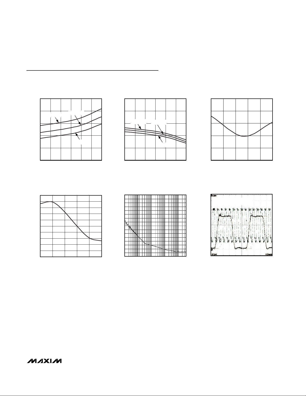
MAX9450 toc01
VOLTAGE (V)
I
DD
(mA)
3.43.33.23.1
48
56
64
72
80
40
3.0 3.63.5
TA = -40°C
TA = +25°C
TA = +85°C
V
DDQ
SUPPLY CURRENT
vs. VOLTAGE
MAX9450 toc02
VOLTAGE (V)
I
DD
(mA)
3.43.33.23.1
48
56
64
72
80
40
3.0 3.63.5
TA = -40°C
TA = +25°C
TA = +85°C
OUTPUT FREQUENCY CHANGE
vs. TEMPERATURE
MAX9450 toc04
TEMPERATURE (°C)
OUTPUT FREQUENCY CHANGE (ppm)
6035-15 10
-30
-20
-10
10
0
20
30
40
50
-50
-40
-40 85
PHASE NOISE
vs. FREQUENCY
MAX9450 toc05
PHASE NOISE (dB)
100k
FREQUENCY (Hz)
1M 10M10k1k
0
-20
-40
-60
-80
-100
-120
-140
-160
OUTPUT RMS JITTER
vs. TEMPERATURE
MAX9450 toc03
TEMPERATURE (°C)
RMS JITTER (ps)
603510-15
2
4
6
8
10
0
-40 85
OUTPUT CLOCK SYNCHRONIZED
TO INPUT REFERENCE
MAX9450 toc06
153.13mV/div
100mV/div
10ns/div
INPUT REFERENCE = 19.44MHz
OUTPUT CLOCK = 155.52 MHz
Typical Operating Characteristics
(VDD= V
DDA
= V
DDQ
= 3.3V. TA= +25°C, unless otherwise noted.)
Page 6

MAX9450/MAX9451/MAX9452
High-Precision Clock Generators
with Integrated VCXO
6 _______________________________________________________________________________________
Pin Description
NAME FUNCTION
1 LOCK Lock Indicator. LOCK goes low when the PLL locks. LOCK is high when the PLL is not locked.
INO_ and IN1_ Select Inputs. Drive SEL0 high to activate IN0; drive SEL1 high to activate IN1. Driving SEL0 and
SEL1 low disables the corresponding input. A 165kΩ pullup resistor pulls SEL0 and SEL1 up to V
DD
.
Differential Reference Input Pair. IN0+ and IN0- accept LVPECL, LVDS, and LVCMOS signals.
V
DD
Digital Power Supply. Connect a 2.4V to 3.6V power supply to VDD. Bypass VDD to GND with a 0.1µF capacitor.
Differential Reference Input Pair. IN1+ and IN1- accept LVPECL, LVDS, and LVCMOS signals.
9 INT Reference Input Condition Indicator. A high indicates a failed reference.
MR Master Reset. Drive MR high to reset all I2C registers to their default state and INT to 0.
Ground and Chip-Select Input. Connect to GND in I2C mode. This is the chip-select input in SPI mode.
SCL Clock Input. SCL is the clock input in I2C bus mode and SPI bus mode.
SDA Data Input. SDA is the data input in I2C bus mode and SPI bus mode.
I2C Address Selection. Drive AD0 and AD1 high to convert the serial interface from I2C to SPI. GND/CS
becomes CS. See Table 3 for the unique addresses list.
CMON Clock Monitor. Drive CMON low to enable the clock monitor. Drive CMON high to disable the clock monitor.
OE
Output Enable Input. Drive OE low to enable the clock outputs. Driving OE high disables the clock outputs, and
the outputs go high impedance. An internal 165kΩ pullup resistor pulls OE up to V
DD
.
V
DDQ
Clock-Output Power Supply. Connect a 2.4V to 3.6V power supply to V
DDQ
for the MAX9450 and MAX9452.
Connect a 1.5V power supply to V
DDQ
for the MAX9451. Connect a 0.1µF bypass capacitor from V
DDQ
to GND.
CLK0-,
Differential Clock Output 0. The MAX9450 features LVPECL outputs. The MAX9451 features HSTL outputs and
the MAX9452 features LVDS outputs.
GND Digital GND
CLK1-,
Differential Clock Output 1. The MAX9450 features LVPECL outputs. The MAX9451 features HSTL outputs, and
the MAX9452 features LVDS outputs.
X1, X2 Reference Crystal Input. Connect the reference crystal from X1 to X2.
V
DDA
Anal og P ow er S up p l y. C onnect a 2.4V to 3.6V p ow er sup p l y to V
D D A
. Byp ass V
D D A
to GN D A w i th a 0.1µF cap aci tor .
External Loop Filter. Connect an RC circuit between LP1 and LP2. See the External Loop Filter section.
GNDA Analog Ground
RJ
Charge-Pump Set Current. Connect an external resistor to GND to set the charge-pump current. See Table 11.
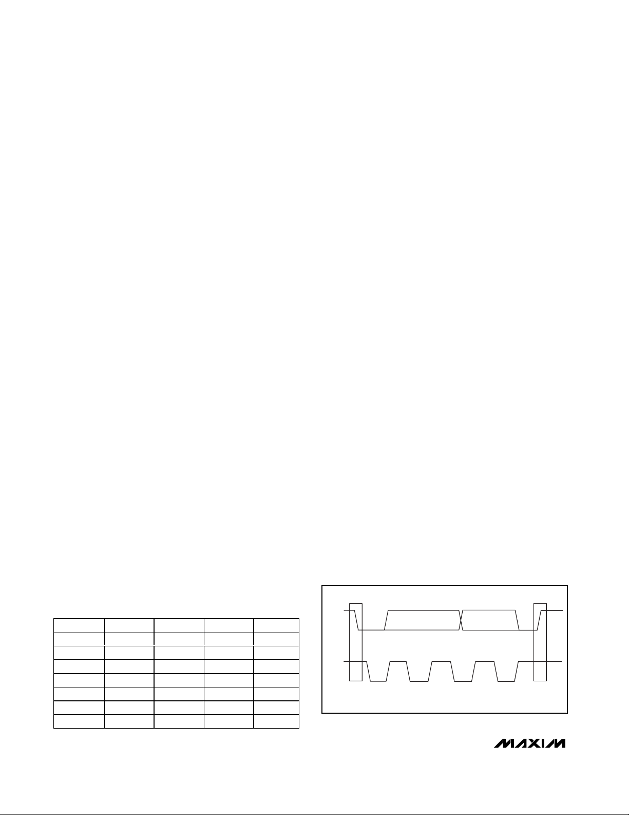
EP Exposed Pad. Connect to ground.
PIN
2, 3 S E L0, S E L1
4, 5 IN0+, IN0-
6, 25
7, 8 IN1+, IN1-
10
11 GND/CS
12
13
14, 15 AD0, AD1
16
17
18, 24
19, 20
CLK0+
21
22, 23
26, 27
29, 30 LP1, LP2
EP
CLK1+
28
31
32
Page 7

MAX9450/MAX9451/MAX9452
High-Precision Clock Generators
with Integrated VCXO
_______________________________________________________________________________________ 7
GNDA
V
DDA
V
DD
GND
VCXO
CRYSTAL
5MHz TO 160MHz
FUNDAMENTAL MODE
AND AT CUT
LOCK DET
1/M
LUT FOR P
LOOP FILTER
RJ
LP2
LP1
X1 X2
I2C PORT
SCL
SDA
LUT FOR N1, N2
LUT FOR M
AD0
AD1
IN0+
IN0-
IN1+
IN1-
SEL0
0
1
CLK
MONITOR
CMON
INT
1/N1
CLK1+
CLK1-
OE
CLK0+
CLK0-
1/N0
1/P
PFD/CP
SEL1
MR
SPI PORT
CONTROL
REGISTERS
GND/CS
MUX
LOCK
12kΩ TO 200k
Ω
DIV0
DIV1
MAX9450
MAX9451
MAX9452
Functional Diagram
Detailed Description
The MAX9450/MAX9451/MAX9452 clock generators
provide high-precision clocks for timing in SONET/SDH
systems or Gigabit Ethernet systems. The MAX9450/
MAX9451/MAX9452 can also provide clocks for the
high-speed and high-resolution ADCs and DACs in 3G
base stations. Additionally, the MAX9450/MAX9451/
MAX9452 can be used as a jitter attenuator for generating high-precision clock signals.
The MAX9450/MAX9451/MAX9452 feature two differential inputs and two differential clock outputs. The inputs
accept LVPECL, LVDS, and LVCMOS signals. The
input reference clock ranges from 8kHz to 500MHz and
the output clock ranges from 15MHz to 160MHz. The
internal clock monitor observes the condition of the
input reference clocks and provides a hitless switch
when an input failure is detected. The MAX9450/
MAX9451/MAX9452 also provide holdover in case no
input clock is supplied.
Control and Status Registers
The MAX9450/MAX9451/MAX9452 contain eight 8-bit
control registers named CR0 to CR7. The registers are
accessible through the I
2
C/SPI interface. CR0 is for the
frequency-dividing factor, P. CR1 and CR2 hold the
values of the divider, M. CR3 and CR4 are for dividers
Page 8

MAX9450/MAX9451/MAX9452
High-Precision Clock Generators
with Integrated VCXO
8 _______________________________________________________________________________________8 ____________________________________________________________________________________________________
N1 and N2, respectively. CR5 and CR6 are the control
function registers for output enabling, reference clock
selection, and activation of the clock monitor and the
holdover function. CR7 contains the status of clock
monitor, holdover, and PLL locking. The addresses of
the eight registers are shown in Table 4. Tables 5
through 10 show the register maps.
Output Buffers
Three different output formats (LVPECL, HSTL, and
LVDS) are available. Each output contains its own
frequency divider. All the output clocks align to their
coincident rising edges. After changing the dividing
ratio, the output clocks complete the current cycle and
stay logic-low until the rising edges of the newly divided
clock. When CR5[7] is high, the MAX9450/MAX9451/
MAX9452 set all the outputs to logic-low. Setting the
bits CR5[6] and CR5[5] properly enables and disables
the outputs individually, see Table 8. A disabled output
is always in high impedance. At the receiver end, the
two cables or PC board traces can be terminated as
shown in Figure 1.
The VCXO output is divided down before driving the output buffers. Program the dividing factor through the serial
interface. The MAX9450/MAX9451/MAX9452 feature two
output dividers DIV0 and DIV1 (see the Functional
Diagram). DIV0 drives OUT0 and either DIV0 or DIV1 can
drive OUT1. CR6[2] sets which divider output drives
OUT1. This function allows for programming OUT1 and
OUT0 to different frequencies.
Reference Clock Inputs
The MAX9450/MAX9451/MAX9452 feature two “anything” differential clock inputs. “Anything” means that
the inputs take any differential signals, such as CML,
LVDS, LVPECL, or HSTL. The inputs can also take a
single-ended input. For example, with LVCMOS reference inputs, connect the inputs to the positive pins
INn+ and connect the negative pins INn- to a reference
voltage of VDD- 1.32V. See Figure 2.
Setting CR5[4] and CR6[3] selects the input reference.
Failure detection and revert function apply only to IN0
and IN1. Also, SEL0 and SEL1 or CR5[3:2] can disable
the corresponding inputs. See Table 2.
Frequency Selection and Programming
The output frequency at CLKn, (n = 0, 1) is determined by
the reference clock and the dividing factors M, Ni (i = 0, 1),
and P, shown in the following equation:
ff
M
Ni P
CLKn REF
=×
×
LVCMOS CLK OUTPUT
V
REF
= VDD - 1.32V
ANYTHING INPUT
Figure 2. Connecting LVCMOS Output to LVPECL Input
Z = 50Ω
LVPECL
OUTPUT
127Ω
127Ω
3.3V
83Ω
83Ω
LVPECL
INPUT
(A) LVPECL DC COUPLING
Z = 50Ω
HSTL
OUTPUT
50Ω
50Ω
HSTL
INPUT
(C) HSTL DC COUPLING
(B) LVDS COUPLING
Z = 50Ω
LVDS
OUTPUT
100Ω
LVDS
INPUT
Figure 1. DC LVPECL, LVDS, and HSTL Termination
Page 9

MAX9450/MAX9451/MAX9452
High-Precision Clock Generators
with Integrated VCXO
_______________________________________________________________________________________ 9
10 GIGABIT ETHERNET SONET
INPUT CLK: 50MHz INPUT CLK: 19.44MHz
CRYSTAL
FREQUENCY
(MHz)
PMNi
OUTPUT
FREQUENCY
(MHz)
CRYSTAL
FREQUENCY
(MHz)
PM
OUTPUT
FREQUENCY
(MHz)
50 2 2 1 50 51.84 1 8 1 51.84
125 2 5 2 62.5 77.76 1 4 1 77.76
125 2 5 1 125 155.52 1 8 1 155.52
— — — — — 155.52 1 4 2 77.76
Table 1. Output Frequency Selection and Register Content Values
where f
CLKn
is the frequency at the CLKn output, f
REF
is the frequency of the reference clock, M (1 to 32,768)
is the dividing factor in the feedback loop, Ni (1, 2, 3, 4,
5, 6, 8, 16) are the dividing factors of the outputs, and P
(1 to 256) is the dividing factor to the input reference
clock. It is possible to set various frequencies at the
two differential CLK_ outputs with this configuration.
For example, in 10 Gigabit Ethernet or SONET applications, set the dividing factors to generate the required
frequencies, as shown in Table 1.
Input Clock Monitor
Failure Detection
The MAX9450/MAX9451/MAX9452 clock-failure-detection function monitors the two reference inputs simultaneously. If a reference input clock signal (IN_) does not
transition for two or more VCO cycles, the device reports
a failure by setting INT high and bit CR7[6] or CR7[5] to
1. See Table 9. After a reference clock failure, the monitor switches to the other valid input reference. At the
same time, the clock monitor loads CR7 with the status of
the reference clocks and which input is selected. The
mapping of CR7 is given in Table 9. If one of the inputs is
disabled according to the bits in CR5[3:2], then the monitor is disabled.
Revert Function
The response of the MAX9450/MAX9451/MAX9452 to a
detected input failure depends on the setting of the
revert function. If the failed input recovers from the
failure, INT and CR7[5:6] resets to 0 if revert is activated. If the recovered input is selected by CR5[4] as the
default input reference, the MAX9450/MAX9451/
MAX9452 reselect this input. If the revert function is not
activated, once an input failure is detected, the monitor
remains in the failure state with INT = 1 and CR7[5:6] =
1, until the MAX9450/MAX9451/MAX9452 are reset.
Activate the revert function using the bit CR5[1].
Failure-Detection Monitor Reset
Reset the fault by toggling CMON from low to high,
toggling MR or CR6[4] from low to high, or by toggling
the bit CR5[0] from low to high. In revert mode, when
the monitor is reset, INT and CR7[5:6] reset to 0 and
the default input is the one indicated by CR5[4].
Holdover Function
The holdover function locks the output frequency to its
nominal value within ±20ppm. Activate this function by
setting CR6[7] to 1. The MAX9450/MAX9451/MAX9452
enter holdover when the devices detect a failure from
both input references. Setting CR6[6] to 1 forces the
device into the holdover state, while resetting CR6[6]
exits holdover.
Use a reset-to-exit holdover. If the revert function is
activated once an input is recovered from the failure,
the device also exits holdover and switches to the
recovered input reference. If both inputs recover simultaneously, the device switches to the default input.
VCXO frequency during holdover is the value of the
frequency right before the failure of inputs.
When CR6[5] goes from 0 to 1, the value of the VCXO
frequency is acquired and stored. The VCXO can be
switched to this acquired frequency by setting CR6[1]
to 1. Such a transition can happen in both the normal
mode of operation and the holdover mode.
PLL Lock Detect
The MAX9450/MAX9451/MAX9452 also feature PLL
lock detection. The MAX9450/MAX9451/MAX9452
compare the frequency of the phase detector input with
the output frequency of the loop frequency divider.
When these two frequencies deviate more than 20ppm,
the LOCK output goes high. At power-up, LOCK is
high. LOCK goes low when the PLL locks. PLL lock
time will also depend on the loop filter bandwidth.
Ni
Page 10
MAX9450/MAX9451/MAX9452
High-Precision Clock Generators
with Integrated VCXO
10 ______________________________________________________________________________________
External Loop Filter
When the device switches from one input reference to
the other or reverts to an input reference from holdover,
the output phase changes smoothly during the transition
using an external PLL filter. The narrower the filter bandwidth is, the smoother the phase transition. However, if
bandwidth is too narrow, it can cause some degradation on output jitter performance.
Charge-Pump Current Setting
The MAX9450/MAX9451/MAX9452 allow external setting
of the charge-pump current in the PLL. Connect a resistor from RJ to GNDA to set the PLL charge-pump current:
charge-pump current (µA) = 2.48 x 1000 /
(R
SET
(kΩ) + 0.375)
where R
SET
is in kΩ and the value of the charge-pump
current is in µA. Use R
SET
to adjust the loop response
to meet individual application requirements. The
charge-pump current and the external filter components change the PLL bandwidth. Table 11 shows the
charge-pump current vs. the resistor’s value.
The loop response equation is defined as:
unity-gain bandwidth = (ICPx R
FILT
x 12kHz) / M
where ICPis the-charge pump current set by REXT,
R
FILT
is the external filter resistance, and M is the feed-
back divider.
Input Disable
The two inputs can be disabled separately by SEL0
and SEL1 or the two bits in CR5[3:2]. Table 2 shows the
state map.
Power-Up and Master Reset
Upon power-up, default frequency divider rates and the
states of the monitor, inputs, and outputs are set
according to Table 10. Setting MR high or CR6[4] to 1
also resets the device. When the device resets, INT
and CR7[5:6] go low and all the registers revert to their
default values.
I2C Interface
The control interface of the MAX9450/MAX9451/MAX9452
is an I2C or SPI depending on the states of AD0 and
AD1. Drive both AD0 and AD1 high to active SPI mode.
Otherwise, I2C is activated. The device operates as a
slave that sends and receives data through the clock
line, SCL, and data line, SDA, to achieve bidirectional
communication with the masters. A master (typically a
microcontroller) initiates all data transfers to and from
slaves, and generates the SCL clock that synchronizes
the data transfer. Figure 4 shows the timing of SCL and
SDA. The SDA line operates as both an input and an
open-drain output. SDA requires a pullup resistor, typically 4.7kΩ. The SCL line operates only as an input. A
pullup resistor, typically 4.7kΩ, is required on SCL if there
are multiple masters on the 2-wire bus, or if the master in
a single-master system has an open-drain SCL output.
I2C Device Address
Every I2C port has a 7-bit device address. This 7-bit
address is the slave (MAX9450/MAX9451/MAX9452)
ID for the master to write and read. In the MAX9450/
MAX9451/MAX9452, the first four bits (1101) of the
address are hard coded into the device at the factory.
See Table 3. The last three bits of the address are input
programmable by the three-level AD0 and AD1. This
configuration provides eight selectable addresses for
the MAX9450/MAX9451/MAX9452, allowing eight
devices to be connected to one master.
Start and Stop Conditions
Both SCL and SDA remain high when the interface is
not busy. The active master signals the beginning of a
transmission with a START (S) condition by transitioning
SDA from high to low while SCL is high. When the master
has finished communicating with the slave, it issues a
STOP (P) condition by transitioning SDA from low to
high while SCL is high. The bus is then free for another
transmission (Figure 3). The interval between a START
and a STOP is called a session.
SEL1 SEL0
CR5[3:2]
IN1 IN0
0000
Disabled
0100
Enabled
1000
Disabled
1100
Enabled
XX01
Enabled
XX10
Disabled
XX11
Enabled
Table 2. Input Activation by SEL0, SEL1,
or CR5[3:2]
SDA
SCL
S
START
CONDITION
P
STOP
CONDITION
Figure 3. Start and Stop Conditions
Disabled
Disabled
Enabled
Enabled
Disabled
Enabled
Enabled
Page 11

MAX9450/MAX9451/MAX9452
High-Precision Clock Generators
with Integrated VCXO
______________________________________________________________________________________ 11
Data Transfer and Acknowledge
Following the START condition, each SCL clock pulse
transfers one bit. Between a START and a STOP, multiple
bytes can be transferred on the 2-wire bus. The first
seven bits (B0–B6) are for the device address. The eighth
bit (B7) indicates the writing (low) or reading (high) operation (W/R). The ninth bit (B8) is the ACK for the address
and operation type. A low ACK bit indicates a successful
transfer; otherwise, a high ACK bit indicates an unsuccessful transfer. The next eight bits (register address),
B9–B16, form the address byte for the control register
to be written (Figure 4). The next bit, bit 17, is the ACK
for the register address byte. The following byte (Data1)
is the content to be written into the addressed register
of the slave. After this, the address counter of I2C is
increased by 1 (Rgst Addr + 1) and the next byte
(Data2) writes into a new register. To read the contents
in the MAX9450/MAX9451/MAX9452’s control registers,
the master sends the register address to be read to the
slave by a writing operation. Then it sends the byte of
device address + R to the slave. The slave (MAX9450/
MAX9451/MAX9452) responds with the content bytes
from the registers, starting from the pointed register to
the last register, CR8, consecutively back to the master
(Figure 5).
SMBCLK
A = START CONDITION
B = MSB OF ADDRESS CLOCKED INTO SLAVE
C = LSB OF ADDRESS CLOCKED INTO SLAVE
D = R/W BIT CLOCKED INTO SLAVE
AB CDEFG
HIJ
SMBDATA
t
SU:STAtHD:STA
t
LOW
t
HIGH
t
SU:DAT
t
SU:STOtBUF
LMK
E = SLAVE PULLS SMBDATA LINE LOW
F = ACKNOWLEDGE BIT CLOCKED INTO MASTER
G = MSB OF DATA CLOCKED INTO SLAVE
H = LSB OF DATA CLOCKED INTO SLAVE
I = MASTER PULLS DATA LINE LOW
J = ACKNOWLEDGE CLOCKED INTO SLAVE
K = ACKNOWLEDGE CLOCK PULSE
L = STOP CONDITION
M = NEW START CONDITION
Figure 5. SMBus Write Timing Diagram
Write Byte Format
Read Byte Format
Send Byte Format
Receive Byte Format
Slave address: equivalent to chip-select line of
a 3-wire interface
Command byte: selects to
which register you are writing
Slave address: equivalent
to chip-select line
Command byte: selects
from which register you
are reading
Slave address: repeated
due to change in dataflow direction
Data byte: reads from
the register set by the
command byte
Command byte: sends command with no data, usually
used for one-shot command
Data byte: reads data from the register
commanded by the last read byte or
write byte transmission; also used for
SMBus alert response return address
S = Start condition Shaded = Slave transmission
P = Stop condition /// = Not acknowledged
Figure 4. I2C Interface Data Structure
S ADDRESS RD ACK DATA /// P
— 7 bits — — 8 bits — —
WRS ACK COMMAND ACK P
— — — 8 bits — —
ADDRESS
7 bits
P
1
ACK
—
DATA
8 bits
ACK
—
COMMAND
8 bits
ACK
—
S ADDRESS WR ACK COMMAND ACK S ADDRESS
7 bits——8 bits——7 bits—
RD—ACK—DATA
8 bits
///
—
P
—
Data byte: data goes into the register
set by the command byte (to set
thresholds, configuration masks, and
sampling rate)
WR
—
ADDRESS
7 bits
S
—
Page 12
MAX9450/MAX9451/MAX9452
High-Precision Clock Generators
with Integrated VCXO
12 ______________________________________________________________________________________
SMBCLK
AB CDEFG HIJ
K
SMBDATA
t
SU:STA
t
HD:STA
t
LOWtHIGH
t
SU:DAT
t
HD:DAT
t
SU:STO
t
BUF
A = START CONDITION
B = MSB OF ADDRESS CLOCKED INTO SLAVE
C = LSB OF ADDRESS CLOCKED INTO SLAVE
D = R/W BIT CLOCKED INTO SLAVE
E = SLAVE PULLS SMBDATA LINE LOW
L
M
F = ACKNOWLEDGE BIT CLOCKED INTO MASTER
G = MSB OF DATA CLOCKED INTO MASTER
H = LSB OF DATA CLOCKED INTO MASTER
I = MASTER PULLS DATA LINE LOW
J = ACKNOWLEDGE CLOCKED INTO SLAVE
K = ACKNOWLEDGE CLOCK PULSE
L = STOP CONDITION
M = NEW START CONDITION
Figure 6. SMBus Read Timing Diagram
t
CSS
t
CSH
f
SCL
t
CSW
CS
SCLK
DIN
t
DS
t
DS
D0D1D14D15
Figure 7. SPI Write Operation Timing Diagram
SLK
SDA
D15
D14
D13 D12
D11 D10
D9
D8
D7 D6
D5 D4
D3
D2 D1
D0
REGISTER ADDRESS
REGISTER DATA
CS
Figure 8. SPI Register Address and Data Configuration Function Setting Tables
SPI Interface
The SPI interface is activated when AD0 = AD1 = high.
The SPI port is a write-only interface, and it uses the
three inputs: CS, SCL, and SDA. Bit D15 is always 0,
indicating the write-only mode, as shown in Figure 5.
D14–D8 are the register address bits and D7–D0 are
the data bits. In Table 4, the register address mapping
is still valid, except the first address bit on the left is not
used. D14 is the LSB of the address, and D7 is the LSB
of the data. D15–D0 are sent with LSB (D15) first. The
maximum SCL frequency is 2MHz.
To perform a write, set D15 = 0, drive CS low, toggle
SCL to latch SDA data on the rising edge, then drive
CS high after 16 SCL cycles for two SCL cycles to signal the boundary of a 16-bit word (Figure 5). SCL must
be low when CS falls at the start of a transmission.
Switching of SCL and SDA is ignored unless CS is low.
Page 13
MAX9450/MAX9451/MAX9452
High-Precision Clock Generators
with Integrated VCXO
______________________________________________________________________________________ 13
AD0 AD1 ADDRESS
Low Low 1101000
Low Open 1101001
Low High 1101010
Open Low 1101011
Open Open 1101100
Open High 1101101
High Low 1101110
High Open 1101111
High High Covert to SPI
Table 3. I2C Address Setting by AD0 and AD1
REGISTER NAME
REGISTER ADDRESS
FUNCTION
CR0 00000000 P divider
CR1 00000001
M divider byte 1
CR2 00000010
M divider byte 2
CR3 00000011 N1 divider
CR4 00000100 N2 divider
CR5 00000101 Control
CR6 00000110 Control
CR7 00000111 Status
CR8 00001000 Reserved
Table 4. I2C and SPI Register Address*
CR0 DIVIDING RATE FOR P
0000-0000 1
0000-0001 2
——
1111-1110 255
1111-1111 256
Table 5. Dividing Rate Setting for P Divider
CR1 CR2[7:1]*
DIVIDING VALUE OF M
0000-0000 0000-000 1
0000-0000 0000-001 2
—— —
1111-1111 0011-110 8191
1111-1111 0011-111 8192
1111-1111 1111-111 32,768
Table 6. Dividing Rate Setting for M Divider
*When the SPI port is activated, the first address bit on the left
is omitted and the remaining seven bits are used. The LSB is
the first bit on the right.
*The last 5 LSBs of CR3[4:0] and CR4[4:0] are reserved.
*CR2[0], the last LSB, is reserved.
CR3*
DIVIDING
CR4*
DIVIDING
VALUE OF N1
1
1
2
2
3
3
4
4
5
5
6
6
8
8
16
16
Table 7. Dividing Rate Setting for N0 and
N1 Divider
VALUE OF N0
000XXXXX
001XXXXX
010XXXXX
011XXXXX
100XXXXX
101XXXXX
110XXXXX
111XXXXX
000XXXXX
001XXXXX
010XXXXX
011XXXXX
100XXXXX
101XXXXX
110XXXXX
111XXXXX
Page 14

MAX9450/MAX9451/MAX9452
High-Precision Clock Generators
with Integrated VCXO
14 ______________________________________________________________________________________
ACTION
DEFAULT
CR0 P = 1 00000000
CR1 M = 1 00000000
CR2 M = 1 00000000
CR3 N0 = 1 00000000
CR4 N1 = 1 00000000
1. Outputs enable
2. IN0 is the default input
3. Both inputs are enabled by
SEL0 and SEL1
4. Monitor is nonrevertive
5. Holdover is disabled
CR5: 01100000
CR6: 00000000
CR7 Status 00000000
CR8 Reserved 00000000
Table 10. Register Default Values at Power-Up
CR5, CR6
FUNCTION STATE
Output disable
0: Outputs are enabled
1: Outputs disabled to logic-low
CLK0 enabling
0: CLK0 is disabled to high impedance (overrides CR5[7] = 1 setting)
1: CLK0 is enabled
CLK1 enabling
0: CLK1 is disabled to high impedance (overrides CR5[7] = 1 setting)
1: CLK1 is enabled
Default input
setting
0: IN0 is the default input
1: IN1 is the default input
Input enabling
00: The selection is controlled by SEL0, SEL1 (see Table 2)
01: Enable IN0, disable IN1
10: Enable IN1, disable IN0
11: Enable both IN0 and IN1
Revert function
0: The function is not activated
1: The function is activated
C LK m oni tor i s r eset i n r ever t m od e: IN T = 0 and C R7[ 7] = 0, and the P LL sw i tches to the d efaul t i np ut
Holdover function
enabling
0: Holdover function is disabled
1: Holdover function is enabled
Forced holdover
0: Holdover is in normal mode
1: Holdover is forced to be activated
As the bit goes from 0 to 1, the current VCXO frequency is taken as the nominal value
Acquiring nominal
As this bit is toggling from 0 to 1, the current VCXO frequency is taking as the nominal holdover
value
Master reset The bit acts at the same as the input MR; CR6[4] = 1, the chip is reset
REF This bit is always set to zero
ODIV select
CR6[2] = 0: DIV0 output drives CLK2
CR6[2] = 1: DIV1 output drives CLK2
Acquire select
CR6[1] = 0 PLL controls the Xtal frequency
CR6[1] = 1 Xtal frequency is controlled by the acquired value (acquired at rising edge of CR6[5])
Reserved —
Table 8. Control Registers and Control Functions
CR7 FUNCTION STATE
Status of IN0
Status of IN1
0: Normal
1: Failure detected
Input clock
0: IN0 is currently used
1: IN1 is currently used
LOCK indicator
1: PLL not locked
0: PLL locked
Holdover status
1: Device is in holdover state
0: Device is in normal state
Reserved —
Table 9. Mapping for the Input Monitor Status
CR5[7]
CR5[6]
CR5[5]
CR5[4]
CR5[3:2]
CR5[1]
CR5[0] CLK monitor reset
CR6[7]
CR6[6]
CR6[5]
CR6[4]
CR6[3]
CR6[2]
CR6[1]
CR6[0]
CR7[6]
CR7[5]
CR7[4]
CR7[3]
CR7[2]
CR7[1:0]
VCXO frequency
selection indicator
REGISTER
CR5, CR6
Page 15

MAX9450/MAX9451/MAX9452
High-Precision Clock Generators
with Integrated VCXO
______________________________________________________________________________________ 15
Applications Information
Crystal Selection
The MAX9450/MAX9451/MAX9452 internal VCXO circuitry requires an external crystal. The frequency of the
crystal ranges from 15MHz to 160MHz, depending on
the application. It is important to use a quartz crystal
that prevents reduction of the frequency pulling range,
temperature stability, or excessive output phase jitter.
Choose an AT-cut crystal that oscillates at the required
frequency on its fundamental mode with a variation of
25ppm, including frequency accuracy and operating
temperature range. Select a crystal with a load capacitance of 8pF and a motional capacitance of at least 7fF
to achieve the specified pulling range.
LVDS Cables and Connectors
The interconnect for LVDS typically has a 100Ω differential impedance. Use cables and connectors that
have matched differential impedance to minimize
impedance discontinuities.
Twisted-pair and shielded twisted-pair cables offer
superior signal quality compared to ribbon cable and
tend to generate less EMI due to magnetic-field-canceling effects. Balanced cables pick up common-mode
noise, which is rejected by the LVDS receiver.
Power-Supply Bypassing
Bypass V
DDA
, VDD, and V
DDQ
to ground with high-frequency, surface-mount ceramic 0.1µF and 0.01µF
capacitors. Place the capacitors as close as possible
to the device with the 0.01µF capacitor closest to the
device pins.
Board Layout
Circuit-board trace layout is very important to maintain
the signal integrity of high-speed differential signals.
Maintaining integrity is accomplished in part by reducing signal reflections and skew and increasing common-mode noise immunity.
Signal reflections are caused by discontinuities in the
50Ω (100Ω for LVDS outputs) characteristic impedance
of the traces. Avoid discontinuities by maintaining the
distance between differential traces, not using sharp
corners or vias. Ensure the two traces are parallel and
close to each other to increase common-mode noise
immunity and reduce EMI. Matching the electrical length
of the differential traces further reduces signal skew.
Output Termination
Terminate the MAX9450 outputs with 50Ω to VCC- 2V
or use an equivalent thevenin termination. When a single-ended signal is taken from a differential output, terminate both outputs.
The MAX9452 outputs are specified for a 100Ω load,
but can drive 90Ω to 132Ω to accommodate various
types of interconnects. The termination resistor at the
driven receiver should match the differential characteristic impedance of the interconnect and be located
close to the receiver input. Use a ±1% surface-mount
termination resistor.
Chip Information
PROCESS: CMOS
RESISTOR (kΩ) CURRENT (µA)
12 200.5
20 121.88
50 49.41
100 24.86
150 16.61
200 12.48
Table 11. Resistor Value vs. Charge-Pump
Current
Page 16
MAX9450/MAX9451/MAX9452
High-Precision Clock Generators
with Integrated VCXO
Maxim cannot assume responsibility for use of any circuitry other than circuitry entirely embodied in a Maxim product. No circuit patent licenses are
implied. Maxim reserves the right to change the circuitry and specifications without notice at any time.
16 ____________________Maxim Integrated Products, 120 San Gabriel Drive, Sunnyvale, CA 94086 408-737-7600
© 2006 Maxim Integrated Products Printed USA is a registered trademark of Maxim Integrated Products, Inc.
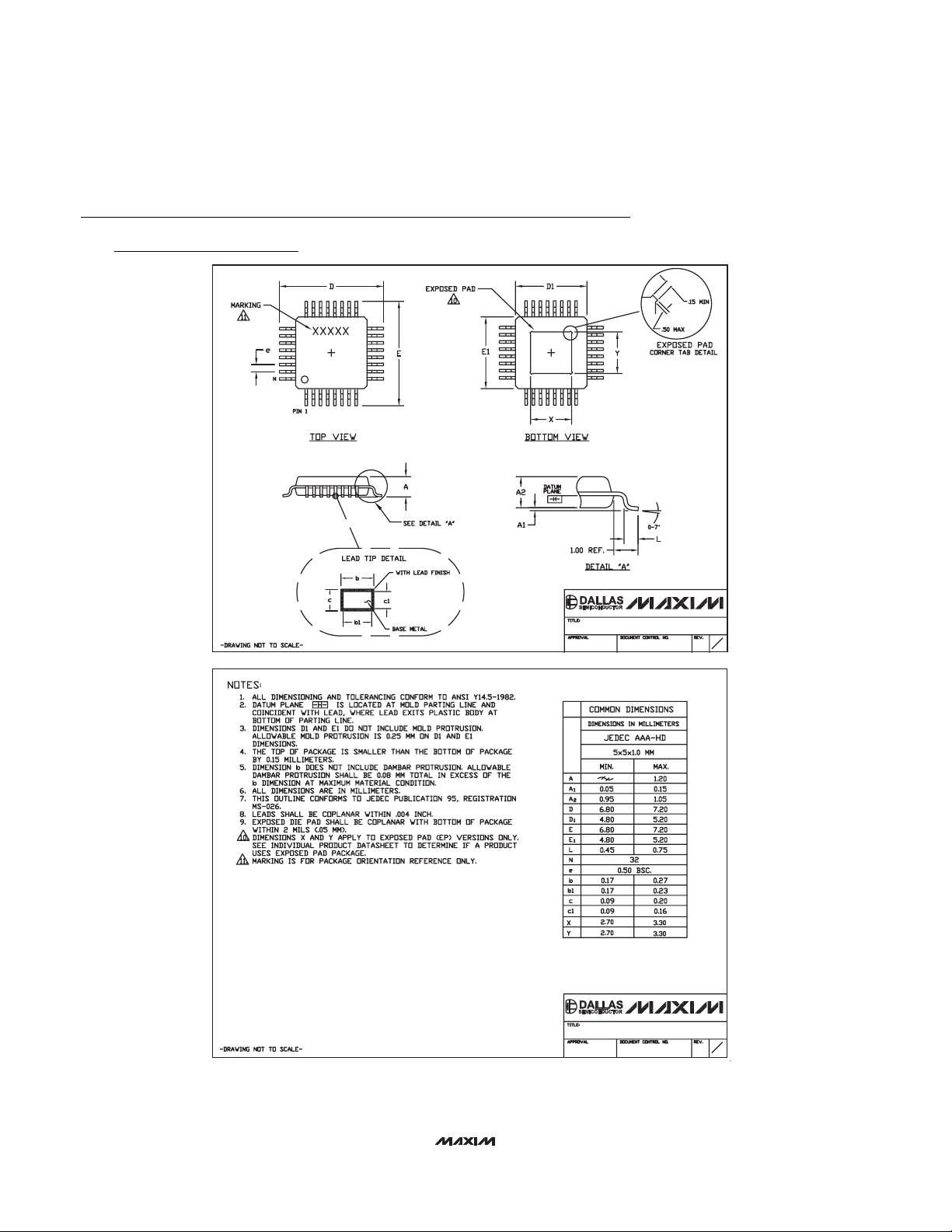
Package Information
(The package drawing(s) in this data sheet may not reflect the most current specifications. For the latest package outline information
go to www.maxim-ic.com/packages
.)
32L,TQFP.EPS
F
1
2
21-0079
PACKAGE OUTLINE,
32L TQFP, 5x5x1.0mm, EP OPTION
F
2
2
21-0079
PACKAGE OUTLINE,
32L TQFP, 5x5x1.0mm, EP OPTION
 Loading...