

Page 1
General Description
The MAX941/MAX942/MAX944 are single/dual/quad
high-speed comparators optimized for systems powered from a 3V or 5V supply. These devices combine
high speed, low power, and Rail-to-Rail®inputs.
Propagation delay is 80ns, while supply current is only
350µA per comparator.
The input common-mode range of the MAX941/
MAX942/MAX944 extends beyond both power-supply
rails. The outputs pull to within 0.4V of either supply rail
without external pullup circuitry, making these devices
ideal for interface with both CMOS and TTL logic. All
input and output pins can tolerate a continuous shortcircuit fault condition to either rail.
Internal hysteresis ensures clean output switching,
even with slow-moving input signals. The MAX941 features latch enable and device shutdown.
The single MAX941 and dual MAX942 are offered in a
tiny µMAX package. Both the single and dual MAX942
are available in 8-pin DIP and SO packages. The quad
MAX944 comes in 14-pin DIP and narrow SO packages.
________________________Applications
3V/5V Systems
Battery-Powered Systems
Threshold Detectors/Discriminators
Line Receivers
Zero-Crossing Detectors
Sampling Circuits
____________________________Features
♦ Available in µMAX Package
♦ Optimized for 3V and 5V Applications
(operation down to 2.7V)
♦ Fast, 80ns Propagation Delay (5mV overdrive)
♦ Rail-to-Rail Input Voltage Range
♦ Low Power:
1mW Power Dissipation per Comparator (3V)
350µA Supply Current
♦ Low, 1mV Offset Voltage
♦ Internal Hysteresis for Clean Switching
♦ Outputs Swing 200mV of Power Rails
♦ CMOS/TTL-Compatible Outputs
♦ Output Latch (MAX941 only)
♦ Shutdown Function (MAX941 only)
MAX941/MAX942/MAX944
High-Speed, Low-Power, 3V/5V, Rail-to-Rail,
Single-Supply Comparators
________________________________________________________________ Maxim Integrated Products 1
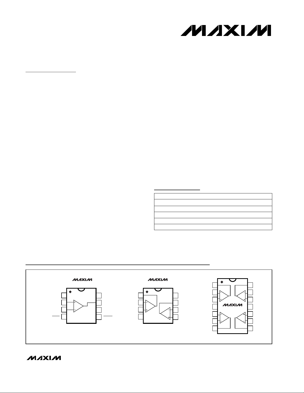
Pin Configurations
19-0229; Rev 4; 9/01
Ordering Information continued at end of data sheet.
8 SO-40°C to +85°CMAX941ESA
8 Plastic DIP-40°C to +85°CMAX941EPA
8 SO0°C to +70°CMAX941CSA
8 Plastic DIP0°C to +70°C
MAX941CPA
PIN-PACKAGETEMP RANGEPART
8 µMAX-40°C to +85°CMAX941EUA
For pricing, delivery, and ordering information, please contact Maxim/Dallas Direct! at
1-888-629-4642, or visit Maxim’s website at www.maxim-ic.com.
Rail-to-Rail is a registered trademark of Nippon Motorola Ltd.
Ordering Information
TOP VIEW
MAX941
+
1
V
2
+
IN
3
IN-
4
SHDN
DIP/SO/µMAX
8
N.C.
7
OUT
6
GND
5
LATCH
OUTA
INA-
INA
GND
+
MAX942
1
2
A
3
4
DIP/SO/µMAX
OUTA
1
INA-
8
+
V
7
OUTB
6
INB-
B
5
+
INB
INA
INB
INB-
OUTB
2
AD
+
3
+
V
4
+
MAX944
5
BC
6
7
DIP/SO
14
13
12
11
10
9
8
OUTD
IND-
IND
GND
INC
INC-
OUTC
+
+
Page 2
MAX941/MAX942/MAX944
High-Speed, Low-Power, 3V/5V, Rail-to-Rail,
Single-Supply Comparators
2 _______________________________________________________________________________________
ABSOLUTE MAXIMUM RATINGS
ELECTRICAL CHARACTERISTICS
(V+ = 2.7V to 6.0V, TA= T
MIN
to T
MAX
, unless otherwise noted. Typical values are at TA= +25°C.) (Note 14)
Stresses beyond those listed under “Absolute Maximum Ratings” may cause permanent damage to the device. These are stress ratings only, and functional
operation of the device at these or any other conditions beyond those indicated in the operational sections of the specifications is not implied. Exposure to
absolute maximum rating conditions for extended periods may affect device reliability.
Power-Supply Ranges
Supply Voltage V+ to GND .............................................+6.5V
Differential Input Voltage ..........................-0.3V to (V+ + 0.3V)
Common-Mode Input Voltage ..................-0.3V to (V+ + 0.3V)
–L—A—T—C—H–
Input (MAX941 only) ....................-0.3V to (V+ + 0.3V)
S—H—D—N–Control Input (MAX941 only) .........-0.3V to (V+ + 0.3V)
Continuous Power Dissipation (T
A
= +70°C)
8-Pin Plastic DIP (derate 9.09mW/°C above +70°C) ...727mW
8-Pin SO (derate 5.88mW/°C above +70°C)................471mW
8-Pin µMAX (derate 4.1mW/°C above +70°C) .............330mW
14-Pin Plastic DIP (derate 10.00mW/°C above +70°C)..800mW
14-Pin SO (derate 8.33mW/°C above +70°C)..............667mW
Operating Temperature Ranges
MAX94_C_ _ .......................................................0°C to +70°C
MAX94_E_ _.....................................................-40°C to +85°C
Storage Temperature Range .............................-65°C to +150°C
Lead Temperature (soldering, 10s) .................................+300°C
MAX94_E
MAX94_C
(Note 1)
(Note 6)
I
SINK
= 4mA
I
SINK
= 400µA
VIN= VOS, VCM= 0 or V+
VIN= VOS, VCM= 0 or
VCM= V+ (Note 4)
I
SOURCE
= 4mA
I
SOURCE
= 400µA
CONDITIONS
µA1I
LEAK
Output Leakage Current
V
0.3 0.4
V
OL
Output Low Voltage
0.2 0.4
V
V+ - 0.4 V+ - 0.3
V
OH
Output High Voltage
V+ - 0.4 V+ - 0.2
V-0.2 V+ + 0.2V
CMR
V2.7 6.0V+Positive Supply Voltage
Input Voltage Range
nA10 100I
OS
Input Offset Current
nA
150 400
I
B
Input Bias Current
150 300
UNITSMIN TYP MAXSYMBOLPARAMETER
13
MAX94_C_ _, MAX94_EP_,
MAX94_ES_
TA= +25°C
VCM= 0 or
VCM= V+
(Note 2)
mV
14
MAX941EUA/MAX942EUA
4
Input-Referred Trip
Points
MAX94_C_ _, MAX94_EP_,
MAX94_ES_
TA= T
MIN
to T
MAX
V
TRIP
mV
6MAX941EUA/MAX942EUA
3
Input Offset Voltage
12
MAX94_C_ _, MAX94_EP_,
MAX94_ES_
MAX94_C_ _, MAX94_EP_,
MAX94_ES_
TA= +25°C
TA= T
MIN
to T
MAX
V
OS
mV
5.5MAX941EUA/MAX942EUA
VCM= 0 or
VCM= V+
(Note 3)
mV
13MAX941EUA/MAX942EUA
µV/V
80 300
MAX94_C_ _, MAX94_EP_,
MAX94_ES_
(Note 5)
80 800
CMRR
Common-Mode Rejection
Ratio
MAX941EUA/MAX942EUA
µV/V
80 300
MAX94_C_ _, MAX94_EP_,
MAX94_ES_
2.7V ≤ V+ ≤ 6.0V,
VCM= 0
80 350
PSRR
Power-Supply Rejection
Ratio
MAX941EUA/MAX942EUA
Page 3
MAX941/MAX942/MAX944
High-Speed, Low-Power, 3V/5V, Rail-to-Rail,
Single-Supply Comparators
_______________________________________________________________________________________ 3
ELECTRICAL CHARACTERISTICS (continued)
(V+ = 2.7V to 6.0V, TA= T
MIN
to T
MAX
, unless otherwise noted. Typical values are at TA= +25°C.) (Note 14)
Note 1: Inferred from the CMRR test. Note also that either or both inputs can be driven to the absolute maximum limit (0.3V
beyond either supply rail) without damage or false output inversion.
Note 2: The input-referred trip points are the extremities of the differential input voltage required to make the comparator output
change state. The difference between the upper and lower trip points is equal to the width of the input-referred hysteresis
zone (see Figure 1).
Note 3: V
OS
is defined as the center of the input-referred hysteresis zone (see Figure 1).
Note 4: The polarity of I
B
reverses direction as VCMapproaches either supply rail. See Typical Operating Characteristics for more
detail.
Note 5: Specified over the full common-mode range (V
CMR
).
Note 6: Applies to the MAX941 only when in shutdown mode. Specification is for current flowing into or out of the output pin for
V
OUT
driven to any voltage from V+ to GND.
Note 7: Typical power dissipation specified with V+ = 3V; maximum with V+ = 6V.
Note 8: Parameter is guaranteed by design and specified with V
OD
= 5mV and C
LOAD
= 15pF in parallel with 400µA of sink or
source current. V
OS
is added to the overdrive voltage for low values of overdrive (see Figure 2).
Note 9: Specified between any two channels in the MAX942/MAX944.
Note 10: Specified as the difference between t
PD+
and t
PD-
for any one comparator.
Note 11: Applies to the MAX941 only for both –S—H—D—N–and–L—A—T—C—H–pins.
Note 12: Applies to the MAX941 only. Comparator is active with –L—A—T—C—H–pin driven high and is latched with –L—A—T—C—H–pin driven low
(see Figure 2).
Note 13: Applicable to the MAX941 only. Comparator is active with –S—H—D—N–pin driven high and is in shutdown with –S—H—D—N–pin driven
low. Shutdown disable time is the delay when –S—H—D—N–is driven high to the time the output is valid.
Note 14: The MAX941EUA and MAX942EUA are 100% production tested at T
A
= +25°C. Specifications over temperature are
guaranteed by design.
PARAMETER
SYMBOL CONDITIONS MIN TYP MAX UNITS
Supply Current per Comparator
380 600
Logic Input Voltage High V
IH
(Note 11) –
V
–2–+– + 0.4 –V–2–+– V
Logic Input Voltage Low V
IL
(Note 11) –
V
–2–+––
V
–2–+– - 0.4 V
Logic Input Current IIL, I
IHVLOGIC
= 0 or V+ (Note 11) 210µA
Data-to-Latch Setup Time t
S
(Note 12) 20 ns
Latch-to-Data Hold Time t
H
(Note 12) 30 ns
Latch Pulse Width t
LPW
MAX941 only 50 ns
Latch Propagation Delay t
LPD
MAX941 only 70 ns
Shutdown Time (Note 13) 3 µs
Shutdown Disable Time (Note 13) 10 µs
Propagation Delay Skew (Note 10) 10 ns
I
CC
V+ = 3V
350 500
MAX941 only, shutdown mode (V+ = 3V) 12 60
µA
1.0 4.2
Power Dissipation per
Comparator
PD (Note 7)
1.0 3.6
mW
Differential Propagation Delay dt
PD
(Note 9) 10 ns
MAX941
MAX942/MAX944
430 700MAX941
V+ = 5V
400 600MAX942/MAX944
MAX941
MAX942/MAX944
MAX94_C
MAX94_E
80 150
Propagation Delay
t
PD+
,
t
PD-
(Note 8)
80 200
ns
Page 4
MAX941/MAX942/MAX944
High-Speed, Low-Power, 3V/5V, Rail-to-Rail,
Single-Supply Comparators
4 _______________________________________________________________________________________
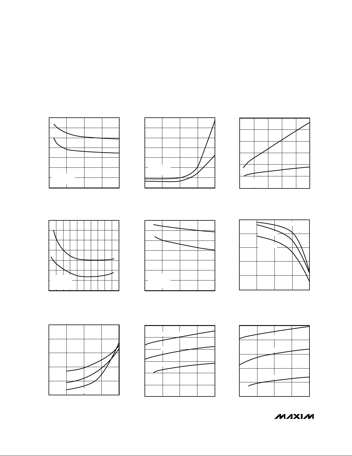
__________________________________________Typical Operating Characteristics
(V+ = 3.0V, TA = +25°C, unless otherwise noted.)
100
40
0 100
PROPAGATION DELAY vs.
INPUT OVERDRIVE
50
90
MAX941-01
INPUT OVERDRIVE (mV)
PROPAGATION DELAY (ns)
75
70
60
25 50
80
30
t
PD+
t
PD-
RS = 10Ω
C
LOAD
= 15pF
400
100
10 100k
PROPAGATION DELAY vs.
SOURCE IMPEDANCE
150
350
MAX941-02
SOURCE IMPEDANCE (Ω)
PROPAGATION DELAY (ns)
10k
250
200
100 1k
300
50
t
PD+
t
PD-
C
LOAD
= 15pF
V
OD
= 5mV
180
60
0
PROPAGATION DELAY vs.
CAPACITIVE LOAD
80
160
MAX941-03
CAPACITIVE LOAD (pF)
PROPAGATION DELAY (ns)
400
120
100
100 300 500
140
200
RS = 10Ω
V
OD
= 5mV
t
PD+
t
PD-
130
-60 -20 40 80
PROPAGATION DELAY vs.
TEMPERATURE
70
110
MAX941-04
TEMPERATURE (°C)
PROPAGATION DELAY (ns)
060
90
120
60
100
80
-40 20 100 120
140
RS = 10Ω
C
LOAD
= 15pF
V
OD
= 5mV
0
1
OUTPUT LOW VOLTAGE
vs. SINK CURRENT
MAX941-07
SINK CURRENT (µA)
V
OL
(V)
0.1
0.2
0.3
0.4
0.5
10 100 1000 10,000
TA = -55°C
TA = +25°C
TA = +125°C
100
40
26
PROPAGATION DELAY vs.
SUPPLY VOLTAGE
50
90
MAX941-05
SUPPLY VOLTAGE (V)
PROPAGATION DELAY (ns)
5
70
60
34
80
30
t
PD+
t
PD-
RS = 10Ω
C
LOAD
= 15pF
V
OD
= 5mV
2.6
1 10,000
OUTPUT HIGH VOLTAGE vs.
SOURCE CURRENT
2.7
MAX941-06
SOURCE CURRENT (µA)
V
OH
(V)
1000
2.9
2.8
10 100
3.0
2.5
TA = +125°C
TA = +25°C
TA = -55°C
MAX941 TOTAL SUPPLY CURRENT
vs. SUPPLY VOLTAGE
SUPPLY CURRENT (µA)
0
2
SUPPLY VOLTAGE (V)
100
200
300
400
500
600
34 5 6
MAX941-08
TA = +125°C
TA = +25°C
TA = -55°C
MAX942 TOTAL SUPPLY CURRENT
vs. SUPPLY VOLTAGE
SUPPLY CURRENT (µA)
300
SUPPLY VOLTAGE (V)
400
500
600
700
800
MAX941-09
TA = +125°C
TA = +25°C
TA = -55°C
23456
Page 5

MAX941/MAX942/MAX944
High-Speed, Low-Power, 3V/5V, Rail-to-Rail,
Single-Supply Comparators
_______________________________________________________________________________________ 5
(°C)
____________________________Typical Operating Characteristics (continued)
(V+ = 3.0V, TA = +25°C, unless otherwise noted.)
MAX944 TOTAL SUPPLY CURRENT
vs. SUPPLY VOLTAGE
2.00
1.75
1.50
1.25
SUPPLY CURRENT (mA)
1.00
0.75
23456
TA = +125°C
TA = +25°C
TA = -55°C
SUPPLY VOLTAGE (V)
VOLTAGE TRIP POINTS/INPUT OFFSET
VOLTAGE vs. TEMPERATURE
1000
V
V
TRIP-
TRIP+
V
OS
500
(µV)
0
OS
-500
-1000
TRIP POINTS / V
-1500
VCM = 0
-2000
-60 140-40 -20 0 20 40 60 80 100 120
TEMPERATURE (°C)
INPUT VOLTAGE RANGE
vs. TEMPERATURE
4
MAX941-10
3
2
1
0
INPUT VOLTAGE RANGE (V)
-1
-60 140-40 -20 0 20 40 60 80 100 120
INPUT BIAS CURRENT/INPUT OFFSET
CURRENT vs. TEMPERATURE
250
MAX941-13
200
150
100
50
INPUT BIAS / OFFSET CURRENT (nA)
0
-60 140-40 -20 0 20 40 60 80 100 120
V
+
CM
V
CM-
TEMPERATURE (°C)
IB+
I
-
B
I
OS
TEMPERATURE (°C)
V+ = 3.0V
MAX941-11
MAX941-14
SHORT-CIRCUIT OUTPUT CURRENT
vs. TEMPERATURE
40
OUTPUT SHORTED
30
20
10
SHORT-CIRCUIT OUTPUT CURRENT (mA)
0
-60 -40 -20 0 20 40 60 80 100 120 140
TO V+ (SINKING)
OUTPUT SHORTED
TO GND (SOURCING)
TEMPERATURE (°C)
INPUT BIAS CURRENT (IB+, IB-)
vs. COMMON-MODE VOLTAGE
(nA)
-
B
+, I
B
I
-100
250
200
150
100
-50
TA = -55°C
TA = +25°C
TA = +125°C
50
0
0123456
COMMON-MODE VOLTAGE (V)
VIN+ = VINNEGATIVE VALUES
REPRESENT CURRENT
FLOWING INTO THE
DEVICE
V+ = 6V
MAX941-12
MAX941 TOC15
MAX941 SHUTDOWN SUPPLY CURRENT
40
vs. TEMPERATURE
V+ = 6.0V
30
20
V+ = 2.7V
10
SHUTDOWN SUPPLY CURRENT (µA)
0
-60 -40 -20 0 20 40 60 80 100 120 140
TEMPERATURE
MAX941 TOC16
V
V+
GND
OS
10MHz RESPONSE
50ns/div
MAX941 TOC 17
INPUT
50mV/div
OUTPUT
1V/div
Page 6
MAX941/MAX942/MAX944
High-Speed, Low-Power, 3V/5V, Rail-to-Rail,
Single-Supply Comparators
6 _______________________________________________________________________________________
_____________________________Typical Operating Characteristics (continued)
(V+ = 3.0V, TA= +25°C, unless otherwise noted.)
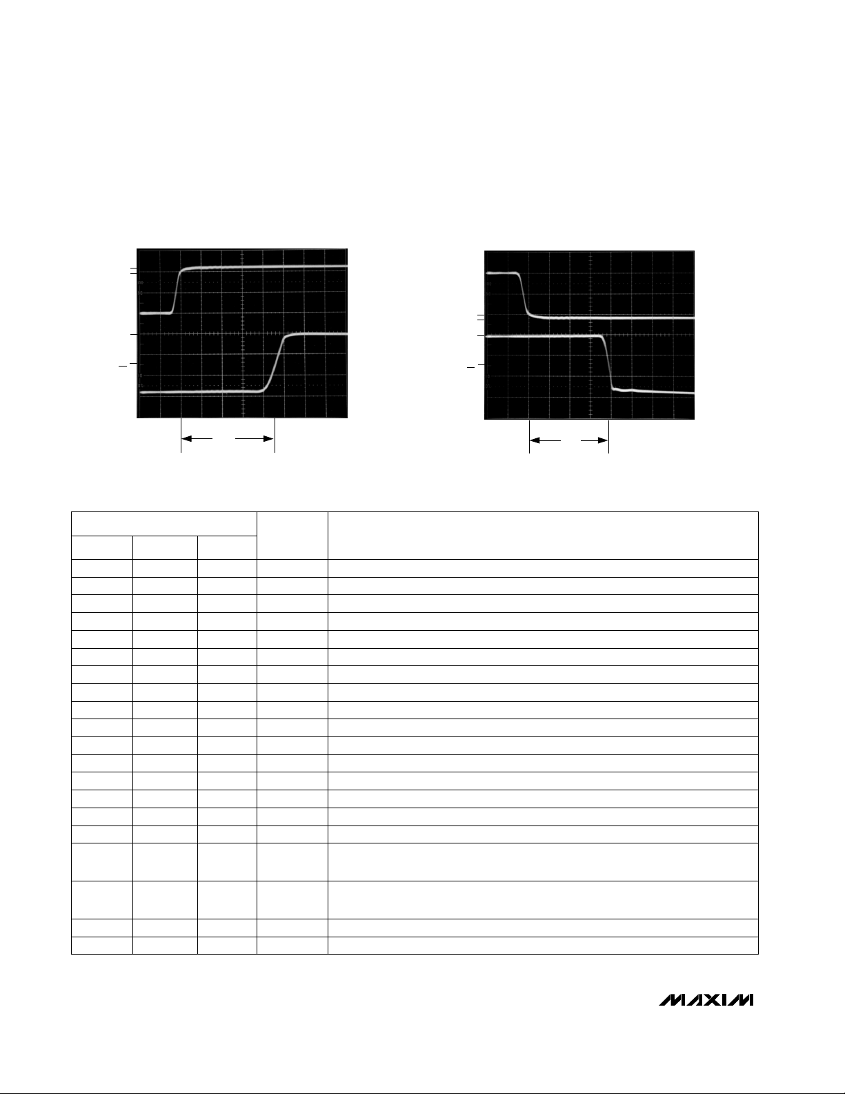
PROPAGATION DELAY (t
PD-
)
INPUT STEP = 100mV
V
OD
= -5mV
INPUT
50mV/div
OUTPUT
1V/div
V
OD
V
OS
V+
V+
2
GND
20ns/div
t
PD-
MAX941 TOC19
NAME FUNCTION
— OUTA Comparator A Output
— INA- Comparator A Inverting Input
______________________________________________________________Pin Description
—
INA+ Comparator A Noninverting Input
1 V+ Positive Supply (V+ to GND must be ≤ 6.5V)
— OUTC Comparator C Output
— OUTB Comparator B Output
— INB- Comparator B Inverting Input
— INB+ Comparator B Noninverting Input
— IND- Comparator D Inverting Input
— IND+ Comparator D Noninverting Input
6 GND Ground
— INC+ Comparator C Noninverting Input
— INC- Comparator C Inverting Input
— OUTD Comparator D Output
2 IN+ Noninverting Input
3 IN- Inverting Input
4 S—H—D—N
–
Shutdown: MAX941 is active when S—H—D—N–is driven high; MAX941 is in shutdown
when S—H—D—N–is driven low.
5 L—A—T—C—H
–
The output is latched when L—A—T—C—H–is low. The latch is transparent when L—A—T—C—H
–
is high.
7 OUT Comparator Output
8 N.C. No Connection. Not internally connected.
3
1
2
8
—
7
6
5
—
—
4
—
—
—
—
—
—
—
—
—
3
1
2
4
PIN
8
7
6
5
13
12
11
10
9
14
—
—
—
—
—
—
MAX944MAX942MAX941
V
OD
V
OS
PROPAGATION DELAY (t
PD+
)
MAX941 TOC18
INPUT
50mV/div
GND
V+
V+
2
20ns/div
t
PD+
INPUT STEP = 100mV
V
= +5mV
OD
OUTPUT
1V/div
Page 7

_______________Detailed Description
The MAX941/MAX942/MAX944 single-supply comparators feature internal hysteresis, high speed, and low
power. Their outputs are guaranteed to pull within 0.4V
of either supply rail without external pullup or pulldown
circuitry. Rail-to-rail input voltage range and low-voltage single-supply operation make these devices ideal
for portable equipment. The MAX941/MAX942/
MAX944 interface directly to CMOS and TTL logic.
Timing
Most high-speed comparators oscillate in the linear
region because of noise or undesired parasitic feedback. This tends to occur when the voltage on one
input is at or equal to the voltage on the other input. To
counter the parasitic effects and noise, the MAX941/
MAX942/MAX944 have internal hysteresis.
The hysteresis in a comparator creates two trip points:
one for the rising input voltage and one for the falling
input voltage (Figure 1). The difference between the trip
points is the hysteresis. When the comparator’s input
voltages are equal, the hysteresis effectively causes
one comparator input voltage to move quickly past the
other, thus taking the input out of the region where
oscillation occurs. Standard comparators require hysteresis to be added with external resistors. The
MAX941/MAX942/MAX944’s fixed internal hysteresis
eliminates these resistors and the equations needed to
determine appropriate values.
Figure 1 illustrates the case where IN- is fixed and IN+
is varied. If the inputs were reversed, the figure would
look the same, except the output would be inverted.
The MAX941 includes an internal latch that allows storage of comparison results. The
L—A—T—C—H
–
pin has a high
input impedance. If L
—A—T—C—H–
is high, the latch is transparent (i.e., the comparator operates as though the latch is
not present). The comparator's output state is stored
when
L—A—T—C—H
–
is pulled low. All timing constraints must
be met when using the latch function (Figure 2).
Shutdown Mode (MAX941 Only)
The MAX941 shuts down when
–S—H—D—N–
is low. When shut
down, the supply current drops to less than 60µA, and
the three-state output becomes high impedance. The
–S—H—D—N–
pin has a high input impedance. Connect
–S—H—D—N–
to V+ for normal operation. Exit shutdown with
L—A—T—C—H
–
high; otherwise, the output will be indeterminate.
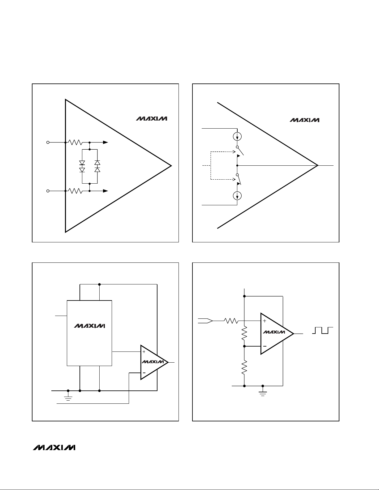
Input Stage Circuitry
The MAX941/MAX942/MAX944 include internal protection circuitry that prevents damage to the precision
input stage from large differential input voltages. This
protection circuitry consists of two back-to-back diodes
between IN+ and IN- as well as two 4.1kΩ resistors
(Figure 3). The diodes limit the differential voltage
applied to the internal circuitry of the comparators to be
no more than 2VF, where VFis the forward voltage drop
of the diode (about 0.7V at +25°C).
For a large differential input voltage (exceeding 2V
F
),
this protection circuitry increases the input bias current
at IN+ (source) and IN- (sink).
Input Current =
(IN+ - IN-) - 2V
F
2 x 4.1kΩ
Input current with large differential input voltages
should not be confused with input bias current (IB). As
long as the differential input voltage is less than 2VF,
this input current is equal to IB. The protection circuitry
also allows for the input common-mode range of the
MAX941/MAX942/MAX944 to extend beyond both
power-supply rails. The output is in the correct logic
state if one or both inputs are within the common-mode
range.
MAX941/MAX942/MAX944
High-Speed, Low-Power, 3V/5V, Rail-to-Rail,
Single-Supply Comparators
_______________________________________________________________________________________ 7
Figure 1. Input and Output Waveform, Noninverting Input
Varied
V
TRIP+
V
V
HYST
V
TRIP-
COMPARATOR
OUTPUT
IN+
V
+ V
TRIP+
V
=
OS
V
= 0
IN-
TRIP-
2
V
OH
V
OL
Page 8

MAX941/MAX942/MAX944
Output Stage Circuitry
The MAX941/MAX942/MAX944 contain a current-driven
output stage as shown in Figure 4. During an output
transition, I
SOURCE
or I
SINK
is pushed or pulled to the
output pin. The output source or sink current is high
during the transition, creating a rapid slew rate. Once
the output voltage reaches VOHor VOL, the source or
sink current decreases to a small value, capable of
maintaining the VOHor VOLstatic condition. This significant decrease in current conserves power after an output transition has occurred.
One consequence of a current-driven output stage is a
linear dependence between the slew rate and the load
capacitance. A heavy capacitive load will slow down a
voltage output transition. This can be useful in noisesensitive applications where fast edges may cause
interference.
__________Applications Information
Circuit Layout and Bypassing
The high gain bandwidth of the MAX941/MAX942/
MAX944 requires design precautions to realize the
comparators’ full high-speed capability. The recommended precautions are:
1) Use a printed circuit board with a good, unbroken, low-inductance ground plane.
2) Place a decoupling capacitor (a 0.1µF ceramic
capacitor is a good choice) as close to V+ as
possible.
3) Pay close attention to the decoupling capacitor’s
bandwidth, keeping leads short.
4) On the inputs and outputs, keep lead lengths
short to avoid unwanted parasitic feedback
around the comparators.
5) Solder the device directly to the printed circuit
board instead of using a socket.
High-Speed, Low-Power, 3V/5V, Rail-to-Rail,
Single-Supply Comparators
8 _______________________________________________________________________________________
Figure 2. MAX941 Timing Diagram with Latch Operator
t
S
t
V+
V
DIFFERENTIAL
INPUT
VOLTAGE
LATCH
OUT
OS
0
V+
V+
2
0
V
OH
V+
2
V
OL
H
t
LPW
t
PD
t
LPD
Page 9
MAX941/MAX942/MAX944
High-Speed, Low-Power, 3V/5V, Rail-to-Rail,
Single-Supply Comparators
_______________________________________________________________________________________ 9
Figure 3. Input Stage Circuitry
Figure 4. Output Stage Circuitry
Figure 5. 3.3V Digitally Controlled Threshold Detector Figure 6. Line Transceiver Application
Ω
IN+
IN–
4.1k
4.1k
Ω
TO INTERNAL
CIRCUITRY
TO INTERNAL
CIRCUITRY
V
DD
= 3.3V
MAX941
MAX942
MAX944
V
CC
I
SOURCE
I
0
SINK
V+ = 3V
MAX941
MAX942
MAX944
OUTPUT
SERIAL
DIGITAL
INPUT
ANALOG IN
VREFC
SDI
GND
8-BIT DAC
MAX512
V
DD
DACOUTC
V
SS
MAX941
COAX LINE
10k
20k
20kΩ
Ω
Ω
MAX941
3V
0
CLEAN
DIGITAL
SIGNAL
Page 10

MAX941/MAX942/MAX944
High-Speed, Low-Power, 3V/5V, Rail-to-Rail,
Single-Supply Comparators
10 ______________________________________________________________________________________
PART TEMP RANGE PIN-PACKAGE
MAX942CPA
0°C to +70°C 8 Plastic DIP
MAX942CSA 0°C to +70°C 8 SO
MAX942EPA -40°C to +85°C 8 Plastic DIP
MAX942ESA
-40°C to +85°C 8 SO
MAX944CPD
0°C to +70°C
14 Plastic DIP
MAX944CSD 0°C to +70°C 14 SO
MAX944EPD
-40°C to +85°C 14 Plastic DIP
MAX944ESD -40°C to +85°C 14 SO
MAX942EUA -40°C to +85°C 8 µMAX
Chip Information
MAX941 TRANSISTOR COUNT: 192
MAX942 TRANSISTOR COUNT: 314
MAX944 TRANSISTOR COUNT: 620
PROCESS: BiPolar
Ordering Information (continued)
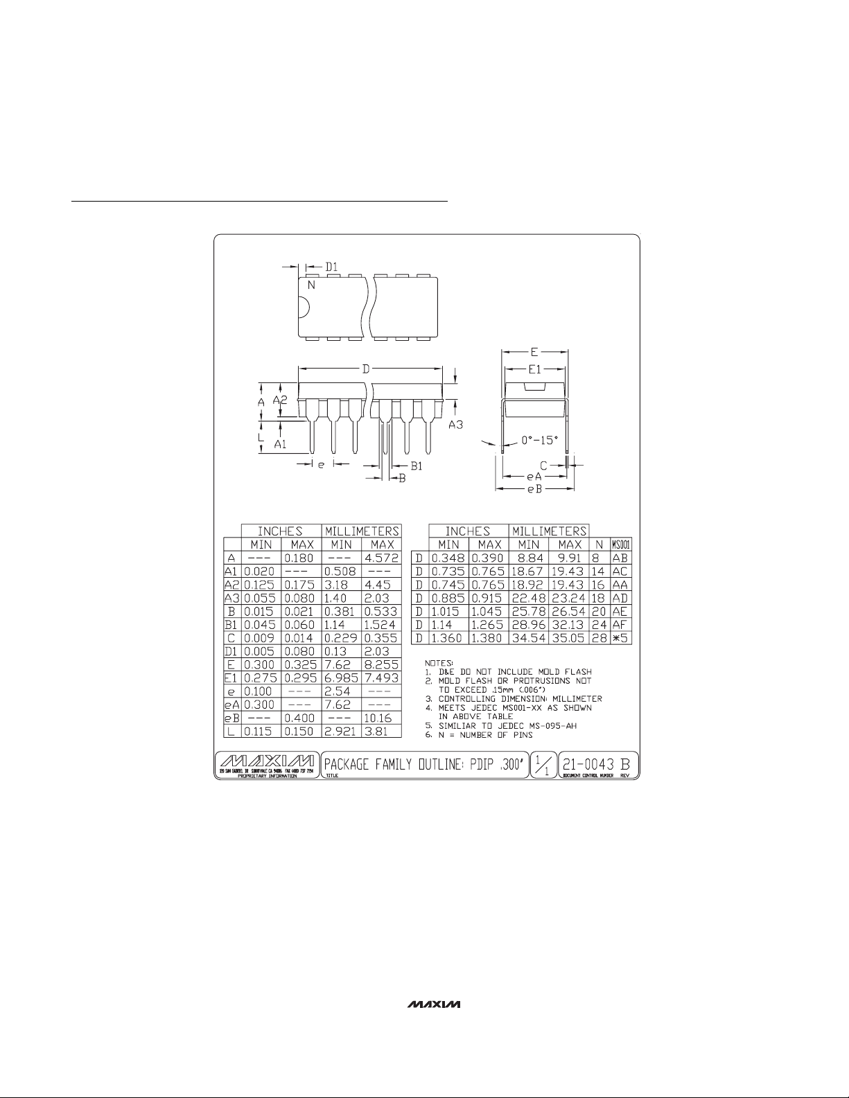
Package Information
8LUMAXD.EPS
Page 11
MAX941/MAX942/MAX944
High-Speed, Low-Power, 3V/5V, Rail-to-Rail,
Single-Supply Comparators
Package Information (continued)
Maxim cannot assume responsibility for use of any circuitry other than circuitry entirely embodied in a Maxim product. No circuit patent licenses are
implied. Maxim reserves the right to change the circuitry and specifications without notice at any time.
Maxim Integrated Products, 120 San Gabriel Drive, Sunnyvale, CA 94086 408-737-7600 ____________________ 11
© 2001 Maxim Integrated Products Printed USA is a registered trademark of Maxim Integrated Products.
PDIPN.EPS
 Loading...