

Page 1
General Description
The MAX9257 serializer pairs with the MAX9258 deserializer to form a complete digital video serial link. The
MAX9257/MAX9258 feature programmable parallel data
width, parallel clock frequency range, spread spectrum,
and preemphasis. An integrated control channel transfers data bidirectionally at power-up during video blanking over the same differential pair used for video data.
This feature eliminates the need for external CAN or LIN
interface for diagnostics or programming. The clock is
recovered from input serial data at MAX9258, hence
eliminating the need for an external reference clock.
The MAX9257 serializes 10, 12, 14, 16, and 18 bits with
the addition of two encoding bits for AC-coupling. The
MAX9258 deserializer links with the MAX9257 to deserialize a maximum of 20 (data + encoding) bits per
pixel/parallel clock period for a maximum serial-data
rate of 840Mbps. The word length can be adjusted to
accommodate a higher pixel/parallel clock frequency.
The pixel clock can vary from 5MHz to 70MHz, depending on the serial-word length. Enabling parity adds two
parity bits to the serial word. The encoding bits reduce
ISI and allow AC-coupling.
The MAX9258 receives programming instructions from
the electronic control unit (ECU) during the control
channel and transmits to the MAX9257 over the serial
video link. The instructions can program or update the
MAX9257, MAX9258, or an external peripheral device,
such as a camera. The MAX9257 communicates with
the peripheral device with I2C or UART.
The MAX9257/MAX9258 operate from a +3.3V core
supply and feature separate supplies for interfacing to
+1.8V to +3.3V logic levels. These devices are available in 40-lead TQFN or 48-pin LQFP packages. These
devices are specified over the -40°C to +105°C temperature range.
Applications
Automotive Cameras
Industrial Cameras
Navigation Systems Display
In-Vehicle Entertainment Systems
Features
♦ 10/12/14/16/18-Bit Programmable Parallel Data
Width
♦ MAX9258 Does Not Require Reference Clock
♦ Parity Protection for Video and Control Channels
♦ Programmable Spread Spectrum
♦ Programmable Rising or Falling Edge for HSYNC,
VSYNC, and Clock
♦ Up to 10 Remotely Programmable GPIO on
MAX9257
♦ Automatic Resynchronization in Case of Loss of
Lock
♦ MAX9257 Parallel Clock Jitter Filter PLL with
Bypass
♦ DC-Balanced Coding Allows AC-Coupling
♦ 5 Levels of Preemphasis for Up to 20m STP Cable
Drive
♦ Integrity Test Using On-Chip Programmable
PRBS Generator and Checker
♦ LVDS I/O Meet ISO10605 ESD Protection (±10kV
Contact and ±30kV Air Discharge)
♦ LVDS I/O Meet IEC61000-4-2 ESD Protection
(±8kV Contact and ±20kV Air Discharge)
♦ LVDS I/O Meet ±200V Machine Model ESD
Protection
♦ -40°C to +105°C Operating Temperature Range
♦ Space-Saving, 40-Pin TQFN (5mm x 5mm) with
Exposed Pad or 48-Pin LQFP Packages
♦ +3.3V Core Supply
MAX9257/MAX9258
Fully Programmable Serializer/Deserializer
with UART/I2C Control Channel
________________________________________________________________
Maxim Integrated Products
1
19-1044; Rev 0; 6/08
For pricing, delivery, and ordering information, please contact Maxim Direct at 1-888-629-4642,
or visit Maxim’s website at www.maxim-ic.com.
EVALUATION KIT
AVAILABLE
Ordering Information
+
Denotes a lead-free package.
*
EP = Exposed pad.
Typical Application Circuit and Pin Configurations appear
at end of data sheet.
PART TEMP RANGE
MAX9257GTL+ -40°C to +105°C 40 TQFN-EP* T4055+1
MAX9257GCM+ -40°C to +105°C 48 LQFP C48+3
MAX9258GCM+ -40°C to +105°C 48 LQFP C48+3
PINPACKAGE
PKG
CODE
Page 2
MAX9257/MAX9258
2 _______________________________________________________________________________________
Fully Programmable Serializer/Deserializer
with UART/I2C Control Channel
ABSOLUTE MAXIMUM RATINGS
Stresses beyond those listed under “Absolute Maximum Ratings” may cause permanent damage to the device. These are stress ratings only, and functional
operation of the device at these or any other conditions beyond those indicated in the operational sections of the specifications is not implied. Exposure to
absolute maximum rating conditions for extended periods may affect device reliability.
VCC_ to GND .........................................................-0.5V to +4.0V
Any Ground to Any Ground...................................-0.5V to +0.5V
SDI+, SDI-, SDO+, SDO- to GND..........................-0.5V to +4.0V
SDO+, SDO- Short Circuit to GND or V
CCLVDS
.........Continuous
DIN[0:15], GPIO[0:9], PCLK_IN, HSYNC_IN, VSYNC_IN,
SCL/TX, SDA/RX, REM to GND............-0.5V to (V
CCIO
+ 0.5V)
DOUT[0:15], PCLK_OUT, HSYNC_OUT, VSYNC_OUT, RX,
LOCK, TX, PD, ERROR, to GND .......-0.5V to (V
CCOUT
+ 0.5V)
Continuous Power Dissipation (T
A
= +70°C)
40-Lead TQFN
Multilayer PCB (derate 35.7mW/°C above +70°C) .....2857mW
48-Lead LQFP
Multilayer PCB (derate 21.7mW/°C above +70°C) .....1739mW
Junction-to-Case Thermal Resistance (θ
JC
) (Note 1)
40-Lead TQFN .............................................................1.7°C/W
48-Lead LQFP...............................................................10°C/W
Junction-to-Ambient Thermal Resistance (θ
JA
) (Note 1)
40-Lead TQFN ..............................................................28°C/W
48-Lead LQFP...............................................................46°C/W
ESD Protection
Human Body Model (R
D
= 1.5kΩ, CS= 100pF)
All Pins to GND ..............................................................±3kV
IEC 61000-4-2 (R
D
= 330Ω, CS= 150pF)
Contact Discharge
(SDI+, SDI-, SDO+, SDO-) to GND................................±8kV
Air Discharge
(SDI+, SDI-, SDO+, SDO-) to GND..............................±20kV
ISO 10605 (R
D
= 2kΩ, CS= 330pF)
Contact Discharge
(SDI+, SDI-, SDO+, SDO-) to GND..............................±10kV
Air Discharge
(SDI+, SDI-, SDO+, SDO-) to GND..............................±30kV
Machine Model (R
D
= 0Ω, CS= 200pF)
All Pins to GND ............................................................±200V
Storage Temperature Range .............................-65°C to +150°C
Junction Temperature......................................................+150°C
Lead Temperature (soldering, 10s) .................................+300°C
MAX9257 DC ELECTRICAL CHARACTERISTICS
(V
CC_
= +3.0V to +3.6V, RL= 50Ω ±1%, TA= -40°C to +105°C, unless otherwise noted. Typical values are at V
CC_
= +3.3V,
T
A
= +25°C.) (Notes 2, 3)
Note 1: Package thermal resistances were obtained using the method described in JDEC specification JESD51-7, using a 4-layer
board. For detailed information on package thermal considerations, refer to www.maxim-ic.com/thermal-tutorial
.
SINGLE-ENDED INPUTS
High-Level Input Voltage V
Low-Level Input Voltage V
Input Current I
Input Clamp Voltage V
SINGLE-ENDED OUTPUTS
High-Level Output Voltage V
PARAMETER SYMBOL CONDITIONS MIN TYP MAX UNITS
0.65 x
V
CCIO
-20 +20
V
-
CCIO
0.1
V
-
CCIO
0.35
IN
CL
OH
V
= +1.71V to +3V
CCIO
V
= +3V to +3.6V 2
IH
IL
CCIO
REM input 2
V
= +1.71V to +3V 0
CCIO
V
= +3V to +3.6V 0 0.8
CCIO
REM input 0 0.8
VIN = 0 to V
V
CCIO
VIN = 0 to V
ICL = -18mA -1.5 V
IOH = -100µA
IOH = -2mA
CCIO
= +1.71V to +3.6V
REM input -20 +20
CC,
V
V
CCIO
0.3
CCIO
0.3
V
CC
0.3
0.3 x
V
CCIO
+
+
+
V
V
µA
V
Page 3
MAX9257/MAX9258
_______________________________________________________________________________________ 3
Fully Programmable Serializer/Deserializer
with UART/I2C Control Channel
MAX9257 DC ELECTRICAL CHARACTERISTICS (continued)
(V
CC_
= +3.0V to +3.6V, RL= 50Ω ±1%, TA= -40°C to +105°C, unless otherwise noted. Typical values are at V
CC_
= +3.3V,
T
A
= +25°C.) (Notes 2, 3)
Low-Level Output Voltage V
Output Short-Circuit Current I
I2C/UART I/O
Input Leakage Current I
High-Level Input Voltage SDA/RX V
Low-Level Input Voltage SDA/RX V
Low-Level Output Voltage
SCL, SDA
LVDS OUTPUTS (SDO+, SDO-)
Differential Output Voltage V
Change in VOD Between
Complimentary Output States
Common-Mode Voltage V
Change in VOS Between
Complimentary Output States
Output Short-Circuit Current I
Magnitude of Differential Output
Short-Circuit Current
CONTROL CHANNEL TRANSCEIVER
Differential Output Voltage V
Input Hysteresis
(Figure 2)
PARAMETER SYMBOL CONDITIONS MIN TYP MAX UNITS
= 100µA 0.1
I
OL
= 2mA 0.3
I
OL
Shorted to GND -44 -10
Shorted to V
VI = V
R
PULLUP
Preemphasis off
(Figure 1)
V
SDO+
V
OD
Differential low-to-high threshold 25 90 135
Differential high-to-low threshold -25 -90 -135
CC_
CC
= 1.6k
Ω
or V
= 0 15 mA
= 0 or 3.6V -15 +15 mA
SDO-
10 44
-1 +1 µA
0.7 x
V
CC
250 350 460 mV
1.050 1.25 1.375 V
250 350 460 mV
ILKG
V
Δ
V
Δ
V
I
OSD
V
HYST+
V
HYST-
OL
OS
IH2
IL2
OL2
OD
OD
OS
OS
OS
OD
0.3 x
V
CC
0.4 V
20 mV
20 mV
V
mA
V
V
mV
Page 4
MAX9257/MAX9258
4 _______________________________________________________________________________________
Fully Programmable Serializer/Deserializer
with UART/I2C Control Channel
MAX9257 DC ELECTRICAL CHARACTERISTICS (continued)
(V
CC_
= +3.0V to +3.6V, RL= 50Ω ±1%, TA= -40°C to +105°C, unless otherwise noted. Typical values are at V
CC_
= +3.3V,
T
A
= +25°C.) (Notes 2, 3)
POWER SUPPLY
Worst-Case Supply Current
(Figure 3)
C
L
Sleep Mode Supply Current I
PARAMETER SYMBOL CONDITIONS MIN TYP MAX UNITS
= 8pF, 12 bits
I
CCW
CCS
±2% spread, preemphasis off,
PRATE = 60MHz, SRATE = 840Mbps
No spread, preemphasis off,
PRATE = 60MHz, SRATE = 840Mbps
N o sp r ead , p r eem p hasi s = 20%,
P RATE = 60M H z, S RATE = 840M b p s
N o sp r ead , p r eem p hasi s = 60%,
P RATE = 60M H z, S RATE = 840M b p s
N o sp r ead , p r eem p hasi s = 100%,
P RATE = 60M H z, S RATE = 840M b p s
±2% spread, preemphasis off,
PRATE = 28.57MHz, SRATE = 400Mbps
No spread, preemphasis off,
PRATE = 28.57MHz, SRATE = 400Mbps
No spread, preemphasis = 100%,
PRATE = 28.57MHz, SRATE = 400Mbps
±2% spread, preemphasis off,
PRATE = 14.29MHz, SRATE = 200Mbps
No spread, preemphasis off,
PRATE = 14.29MHz, SRATE = 200Mbps
No spread, preemphasis = 100%,
PRATE = 14.29MHz, SRATE = 200Mbps
±2% spread, preemphasis off,
PRATE = 7.14MHz, SRATE = 100Mbps
No spread, preemphasis off,
PRATE = 7.14MHz, SRATE = 100Mbps
N o sp r ead , p r eem p hasi s = 100%,
P RATE = 7.14M H z, S RATE = 100M b p s
±2% spread, preemphasis off,
PRATE = 5MHz, SRATE = 70Mbps
No spread, preemphasis off,
PRATE = 5MHz, SRATE = 70Mbps
No spread, preemphasis = 100%,
PRATE = 5MHz, SRATE = 70Mbps
Sleep mode 92 µA
104 126
99 121
99 120
108 127
110 129
78 96
77 94
86 105
55 68
54 67
59 73
44 55
43 54
46 57
34 43
34 42
36 45
mA
Page 5
MAX9257/MAX9258
_______________________________________________________________________________________ 5
Fully Programmable Serializer/Deserializer
with UART/I2C Control Channel
MAX9257 AC ELECTRICAL CHARACTERISTICS
(V
CC_
= +3.0V to +3.6V, RL= 50Ω ±1%, TA= -40°C to +105°C, unless otherwise noted. Typical values are at V
CC_
= +3.3V,
T
A
= +25°C.) (Notes 5, 9)
PCLK_IN TIMING REQUIREMENTS
Clock Period t
Clock Frequency f
Clock Duty Cycle DC t
Clock Transition Time tR, t
SWITCHING CHARACTERISTICS
LVDS Output Rise Time t
LVDS Output Fall Time t
Control Transceiver Transition
Time
Input Setup Time t
Input Hold Time t
Parallel-to-Serial Delay
PLL Lock Time t
Random Jitter t
Deterministic Jitter t
SCL/TX, SDA/RX
Rise Time t
Fall Time t
Pulse Width of Spike Suppressed
in SDA
Data Setup Time t
Data Hold Time t
I2C TIMING (Note 8)
Maximum SCL Clock Frequency f
Minimum SCL Clock Frequency f
Start Condition Hold Time t
PARAMETER SYMBOL CONDITIONS MIN TYP MAX UNITS
T
CLK
F
R
F
t
R1A , tF1A
t
R2 , tF2
t
R1B , tF1B
S
H
t
PSD1
t
PSD2
LOCK
RJ
DJ
RS
FS
1/t
T
HIGH/tT
or t
LOW
/t
T
(Figure 7) 4 ns
20% to 80% (Figure 4) 315 370 ps
20% to 80% (Figure 4) 315 370 ps
20% to 80% (Figure 16)
(Figure 5) 0 ns
(Figure 5) 3 ns
Spread off (Figure 6)
±4% spread
Combined FPLL and SPLL; PCLK_IN stable
420MHz LVDS output, spread off,
FPLL = bypassed
18
2
- 1 PRBS, SRATE = 840Mbps, 18 bits,
no spread
0.3 x VCC to 0.7 x
, CL = 30pF
V
CC
0.7 x VCC to 0.3 x V
R
R
CC, CL
= 10k
PULLUP
= 1.6k
PULLUP
= 30pF 40 ns
14.28 200.00 ns
5 70 MHz
35 50 65 %
642 970 1390
810 1140 1420
290 386 490
Ω
Ω
95kbps to 400kbps 100
t
SPK
400kbps to 1000kbps 50
1000kbps to 4250kbps 10
DC to 10Mbps (bypass mode) 10
SETUP
HOLD
SCL
SCL
HD:STA
400kbps 100
4.25Mbps, CL = 10pF 60
400kbps 100
4.25Mbps, CL = 10pF 0
(Figure 30) 0.6 µs
ps
(4.55 x t
( 36.55 x t
T) +
11
T) +
11
32,768 x
t
T
12
ns
ns
ps
(RMS)
142 ps (p-p)
400
60
ns
ns
ns
ns
4.25 MHz
95 kHz
Page 6
MAX9257/MAX9258
6 _______________________________________________________________________________________
Fully Programmable Serializer/Deserializer
with UART/I2C Control Channel
MAX9257 AC ELECTRICAL CHARACTERISTICS (continued)
(V
CC_
= +3.0V to +3.6V, RL= 50Ω ±1%, TA= -40°C to +105°C, unless otherwise noted. Typical values are at V
CC_
= +3.3V,
T
A
= +25°C.) (Notes 5, 9)
MAX9258 DC ELECTRICAL CHARACTERISTICS
(V
CC_
= +3.0V to +3.6V, RL= 50Ω ±1%, differential input voltage |VID| = 0.05V to 1.2V, input common-mode voltage VCM= |VID/2| to
V
CC
- |VID/2|, TA= -40°C to +105°C, unless otherwise noted. Typical values are at V
CC_
= +3.3V, |VID| = 0.2V, VCM= 1.2V,
T
A
= +25°C.) (Notes 2, 3)
Low Period of SCL Clock t
High Period of SCL Clock t
Repeated START Condition
Setup Time
Data Hold Time t
Data Setup Time t
Setup Time for STOP Condition t
Bus Free Time t
SINGLE-ENDED INPUTS
High-Level Input Voltage V
Low-Level Input Voltage V
Input Current I
Input Clamp Voltage V
SINGLE-ENDED OUTPUTS
High-Level Output Voltage V
Low-Level Output Voltage V
High-Impedance Output Current I
Output Short-Circuit Current I
OPEN-DRAIN OUTPUTS
Output Low Voltage V
Output Low Voltage V
Leakage Current I
LVDS INPUTS (SDI+, SDI-)
Differential Input High Threshold V
Differential Input Low Threshold V
Input Current I
Power-Off Input Current I
CONTROL CHANNEL TRANSCEIVER
Differential Output Voltage V
PARAMETER SYMBOL CONDITIONS MIN TYP MAX UNITS
LOW
HIGH
t
SU:STA
HD:DAT
SU:DAT
SU:STO
BUF
(Figure 30) 1.1 µs
(Figure 30) 0.6 µs
(Figure 30) 0.5 µs
(Figure 30) 0 0.9 µs
(Figure 30) 100 ns
(Figure 30) 0.5 µs
(Figure 30) 1.1 µs
PARAMETER SYMBOL CONDITIONS MIN TYP MAX UNITS
IH
IL
IN
CL
VIN = 0 to V
ICL = -18mA -1.5 V
IOH = -100µA
OH
IOH = -2mA
OL
OZ
OS
OL
OL
LEAK
TH
IN+, IIN-
INO+, IINO-VCC_
OD
IOL = 100µA 0.1
IOL = 2mA 0.3
PD = low, VO = 0 to V
VO = 0V (Note 4) -16 -65
PCLK_OUT, VO = 0V -22 -80
V
CCOUT
V
CCOUT
VO = 0 or V
TL
CC
CCOUT
TXIN -60 +60
PD -20 +20
= +3V, IOL = 6.4mA 0.55 V
= +1.71V, IOL = 1.95mA 0.3 V
CC
= 0 or open -70 +70 µA
2.0 V
00.8V
V
CCOUT
-
0.1
V
CCOUT
-
0.35
-1 +1 µA
-50 mV
-60 +60 µA
250 460 mV
CC
V
µA
V
V
mA
1µA
50 mV
Page 7
MAX9257/MAX9258
_______________________________________________________________________________________ 7
Fully Programmable Serializer/Deserializer
with UART/I2C Control Channel
MAX9258 DC ELECTRICAL CHARACTERISTICS (continued)
(V
CC_
= +3.0V to +3.6V, RL= 50Ω ±1%, differential input voltage |VID| = 0.05V to 1.2V, input common-mode voltage VCM= |VID/2| to
V
CC
- |VID/2|, TA= -40°C to +105°C, unless otherwise noted. Typical values are at V
CC_
= +3.3V, |VID| = 0.2V, VCM= 1.2V,
T
A
= +25°C.) (Notes 2, 3)
MAX9258 AC ELECTRICAL CHARACTERISTICS
V
CC_
= +3.0V to +3.6V, RL= 50Ω ±1%, CL= 8pF, differential input voltage |VID| = 0.1V to 1.2V, input common-mode voltage
V
CM
= |VID/2| to VCC- |VID/2|, TA= -40°C to +105°C, unless otherwise noted. Typical values are at V
CC_
= +3.3V, |VID| = 0.2V, VCM=
1.2V, T
A
= +25°C. (Notes 5, 6, and 7)
Input Hysteresis
(Figure 2)
POWER SUPPLY
Worst-Case Supply Current
C
L
(Figure 8)
Power-Down Supply Current I
PARAMETER SYMBOL CONDITIONS MIN TYP MAX UNITS
= 8pF, 12 bits
V
HYST+
V
HYST-
I
CCW
CCZ
Differential low-to-high threshold 25 90 135
Differential high-to-low threshold -25 -90 -135
±4% spread, PRATE = 60MHz,
SRATE = 840Mbps
Spread off, PRATE = 60MHz,
SRATE = 840Mbps
±4% spread, PRATE = 28.57MHz,
SRATE = 400Mbps
Spread off, PRATE = 28.57MHz,
SRATE = 400Mbps
±4% spread, PRATE = 14.29MHz,
SRATE = 200Mbps
Spread off, PRATE = 14.29MHz,
SRATE = 200Mbps
±4% spread, PRATE = 5MHz,
SRATE = 70Mbps
Spread off, PRATE = 5MHz,
SRATE = 70Mbps
PD = low 10 50 µA
85 128
71 115
67 102
57 84
55 82
46 67
42 57
34 49
mV
mA
PARAMETER SYMBOL CONDITIONS MIN TYP MAX UNITS
SWITCHING CHARACTERISTICS
Output Transition Time t
Output Transition Time,
PCLK_OUT
Output Transition Time t
Output Transition Time,
PCLK_OUT
t
Control Channel Transition Time
Control Channel Transition Time t
PCLK_OUT High Time t
PCLK_OUT Low Time t
R1A, tF1A,
t
R1B, tF1B
R, tF
t
R, tF
R, tF
t
R, tF
R2, tF2
HIGH
LOW
(Figure 9) 0.7 2.2 ns
(Figure 9) 0.5 1.5 ns
V
V
(Figure 16) 0.5 1.2 ns
(Figure 16) 0.6 1.3 ns
(Figure 10)
(Figure 10)
= 1.71V (Figure 9) 1.0 2.8 ns
CCOUT
= 1.71V (Figure 9) 0.7 2.2 ns
CCOUT
0.4 x
t
T
0.4 x
t
T
0.6 x
0.6 x
t
t
T
T
ns
ns
Page 8
MAX9257 SUPPLY CURRENT
vs. FREQUENCY
MAX9257/58 toc01
PCLK FREQUENCY (MHz)
SUPPLY CURRENT (mA)
20 4025 3515 3010
20
40
60
80
100
120
0
545
PRBS PATTERN
18-BIT
100% PREEMPHASIS
NO PREEMPHASIS
MAX9257 SUPPLY CURRENT
vs. FREQUENCY
MAX9257/58 toc02
PCLK FREQUENCY (MHz)
SUPPLY CURRENT (mA)
5515 45
60
40
20
80
100
120
140
0
57535 6525
PRBS PATTERN
10-BIT
100% PREEMPHASIS
NO PREEMPHASIS
MAX9258 SUPPLY CURRENT
vs. FREQUENCY
MAX9257/58 toc03
PCLK FREQUENCY (MHz)
SUPPLY CURRENT (mA)
4010 3515
40
20
60
80
100
120
0
5452520 30
PRBS PATTERN
18-BIT
4% SPREAD
NO SPREAD
Typical Operating Characteristics
(V
CC_
= +3.3V, RL= 50Ω, CL= 8pF, TA= +25°C, unless otherwise noted.)
MAX9257/MAX9258
8 _______________________________________________________________________________________
Fully Programmable Serializer/Deserializer
with UART/I2C Control Channel
MAX9258 AC ELECTRICAL CHARACTERISTICS (continued)
V
CC_
= +3.0V to +3.6V, RL= 50Ω ±1%, CL= 8pF, differential input voltage |VID| = 0.1V to 1.2V, input common-mode voltage
V
CM
= |VID/2| to VCC- |VID/2|, TA= -40°C to +105°C, unless otherwise noted. Typical values are at V
CC_
= +3.3V, |VID| = 0.2V, VCM=
1.2V, T
A
= +25°C. (Notes 5, 6, and 7)
Note 2: Current into a pin is defined as positive. Current out of a pin is defined as negative. All voltages are referenced to ground
except V
TH
and VTL.
Note 3: Maximum and minimum limits over temperature are guaranteed by design and characterization. Devices are production
tested at T
A
= +105°C.
Note 4: One output at a time.
Note 5: AC parameters are guaranteed by design and characterization, and are not production tested.
Note 6: C
L
includes probe and test jig capacitance.
Note 7: t
T
is the period of the PCLK_OUT.
Note 8: For high-speed mode timing, see the
Detailed Description
section.
Note 9: I
2
C timing parameters are specified for fast-mode I2C. Max data rate = 400kbps.
PARAMETER SYMBOL CONDITIONS MIN TYP MAX UNITS
Data Valid Before PCLK_ OUT t
Data Valid After PCLK_OUT t
Serial-to-Parallel Delay
Power-Up Delay t
Power-Down to High Impedance t
DVB
DVA
t
SPD1
t
SPD2
PUD
PDD
(Figure 11)
(Figure 11)
Spread off (Figure 14) 8t
±4% spread 40t
(Figure 12) 100 ns
(Figure 13) 100 ns
Each half of the UI, 12 bit,
Jitter Tolerance t
JT
SRATE = 840Mbps, PRBS
No spread 0.25 0.30 UI
pattern (Figure 15)
0.35 x
t
T
0.35 x
t
T
ns
ns
T
ns
T
Page 9
MAX9257/MAX9258
_______________________________________________________________________________________ 9
Typical Operating Characteristics (continued)
(V
CC_
= +3.3V, RL= 50Ω, CL= 8pF, TA= +25°C, unless otherwise noted.)
Fully Programmable Serializer/Deserializer
with UART/I2C Control Channel
MAX9258 SUPPLY CURRENT
vs. FREQUENCY
120
PRBS PATTERN
10-BIT
100
80
60
40
SUPPLY CURRENT (mA)
20
0
4% SPREAD
5452520 30
PCLK FREQUENCY (MHz)
MAX9257 OUTPUT POWER
SPECTRUM vs. PCLK FREQUENCY
20
10kHz BW
10
4% SPREAD
0
-10
-20
-30
-40
-50
-60
OUTPUT POWER SPECTRUM (dBm)
-70
-80
18 2220
PCLK FREQUENCY (MHz)
900
NO SPREAD
4010 3515
NO SPREAD
2% SPREAD
2119
BIT ERROR RATE (< 10-9) vs.
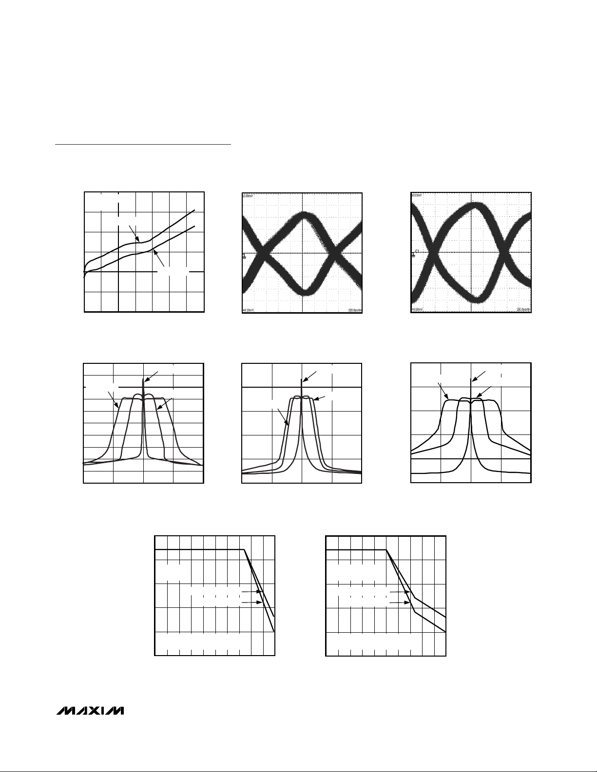
CABLE LENGTH
SERIAL LINK SWITCHING PATTERN WITHOUT
PREEMPHASIS (BIT RATE = 840MHz, 2m STP CABLE)
MAX9257/58 toc04
MAX9257 OUTPUT POWER
SPECTRUM vs. PCLK FREQUENCY
20
10kHz BW
0
MAX9257/58 toc07
1.5% SPREAD
-20
-40
-60
OUTPUT POWER SPECTRUM (dBm)
-80
38 4642
NO SPREAD
PCLK FREQUENCY (MHz)
900
PREEMPHASIS (BIT RATE = 840MHz, 2m STP CABLE)
MAX9257/58 toc05
2% SPREAD
4440
MAX9257/58 toc08
OUTPUT POWER SPECTRUM (dBm)
BIT ERROR RATE (< 10-9) vs.
CABLE LENGTH
SERIAL LINK SWITCHING PATTERN WITH
(PREEMPHASIS = 100%)
MAX9258 OUTPUT POWER
SPECTRUM vs. PCLK FREQUENCY
20
10kHz BW
4% SPREAD
0
-20
-40
-60
-80
38 4642
PCLK FREQUENCY (MHz)
NO SPREAD
2% SPREAD
4440
MAX9257/58 toc06
MAX9257/58 toc09
800
NO SPREAD
STP CABLE
700
600
SERIAL-DATA RATE (Mbps)
500
BER CAN BE AS LOW AS 10
CABLE LENGTHS LESS THAN 10m.
400
0862 4 10 12 14 16 18 20
100% PREEMPHASIS
NO PREEMPHASIS
-12
CABLE LENGTH (m)
MAX9257/58 toc10
FOR
800
2% SPREAD ON
MAX9257, STP CABLE
700
100% PREEMPHASIS
600
SERIAL-DATA RATE (Mbps)
500
400
NO PREEMPHASIS
BER CAN BE AS LOW AS 10
CABLE LENGTHS LESS THAN 10m.
0862 4 10 12 14 16 18 20
CABLE LENGTH (m)
-12
FOR
MAX9257/58 toc11
Page 10
MAX9257/MAX9258
10 ______________________________________________________________________________________
Fully Programmable Serializer/Deserializer
with UART/I2C Control Channel
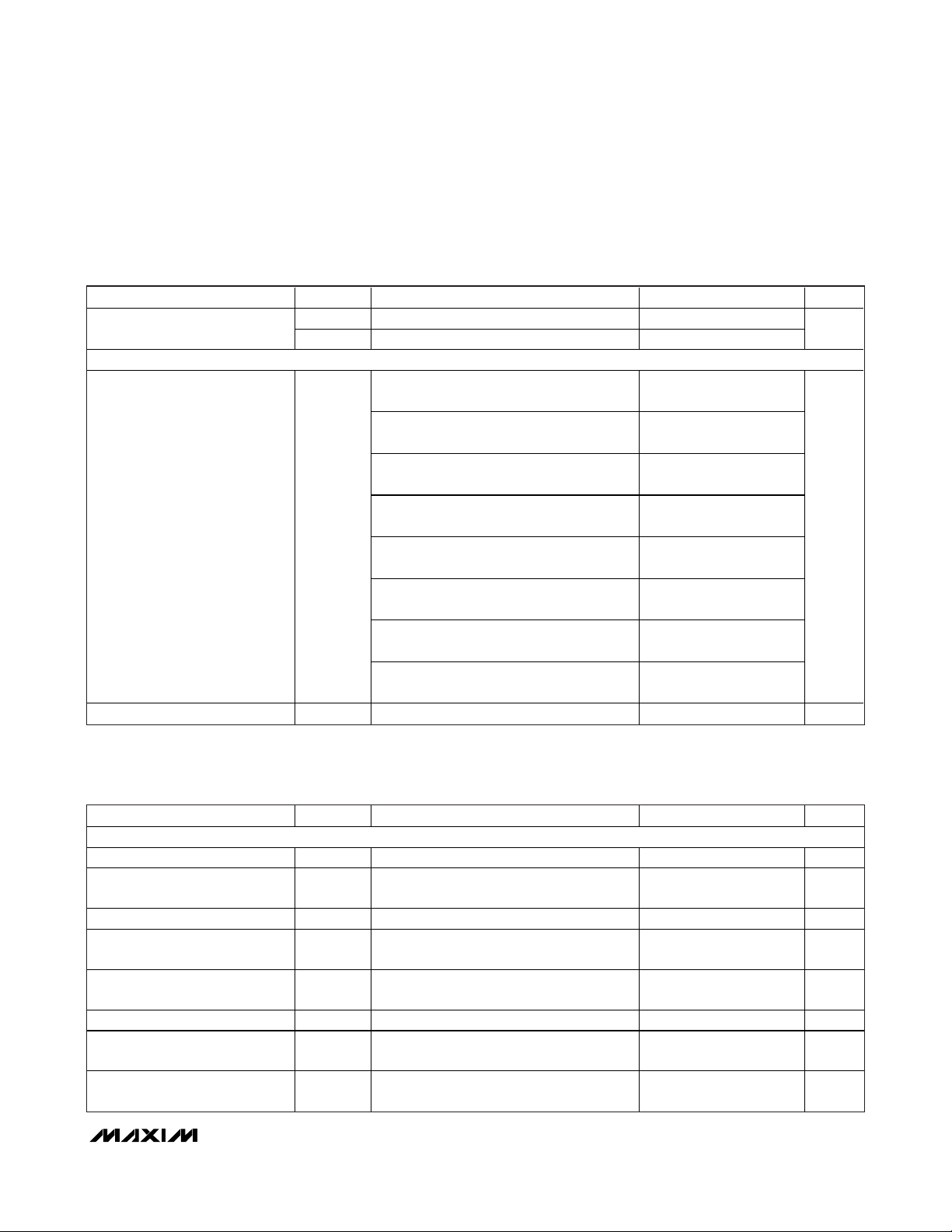
MAX9257 Pin Description
PIN
TQFN LQFP
1, 18 2, 21 V
2, 11,
19, 34
3–8 4–9
9 10 GND
10 11 V
12 15 DIN15/GPIO7
13 16 HSYNC_IN Horizontal SYNC Input. HSYNC_IN is internally pulled down to ground.
14 17 VSYNC_IN Vertical SYNC Input. VSYNC_IN is internally pulled down to ground.
15 18 PCLK_IN
16 19 SCL/TX
17 20 SDA/RX
20, 33 23, 40 V
21 26 GPIO8 General Purpose Input/Output
22 27 GPIO9 General Purpose Input/Output
23 28 V
24 29 GND
25 30 GND
26 31 SDO- Serial LVDS Inverting Output
27 32 SDO+ Serial LVDS Noninverting Output
28 33 V
3, 14,
22, 41
NAME FUNCTION
Single-Ended Input/Output Buffer Supply Voltage. Bypass V
CCIO
GND Digital Supply Ground
DIN[9:14]/
GPIO[1:6]
FPLL
CCFPLL
CC
CCSPLL
SPLL
LVDS
CCLVDS
0.001µF capacitors in parallel as close as possible to the device with the smallest value
capacitor closest to V
Data Input/General Purpose Input/Output. When a serial-data word is less than 18 bits
word length, DIN_ not programmed as data inputs becomes GPIO (Table 22). DIN[9:14]
are internally pulled down to ground.
Filter PLL Ground
Filter PLL Supply Voltage. Bypass V
in parallel as close as possible to the device with the smallest value capacitor closest to
V
Data Input/General Purpose Input/Output. When a serial-data word is less than 18 bits
word length, DIN_ not programmed as data input becomes GPIO (Table 22). DIN15 is
internally pulled down to ground.
Parallel Clock Input. PCLK_IN latches data and sync inputs and provides the PLL reference
clock. PCLK_IN is internally pulled down to ground.
O p en- D r ai n C ontr ol C hannel Outp ut. S C L/TX b ecom es S C L outp ut w hen U ART- to- I
acti ve. S C L/TX b ecom es TX outp ut w hen U ART- to- I
Open-Drain Control Channel Input/Output. SDA/RX becomes bidirectional SDA when
UART-to-I2C is active. SDA/RX becomes RX input when UART-to-I2C is bypassed. SDA
output requires a pullup to V
Digital Supply Voltage. Bypass VCC to ground with 0.1µF and 0.001µF capacitors in p ar al l el
as cl ose as p ossi b l e to the d evi ce w i th the sm al l est val ue cap aci tor cl osest to V
Spread PLL Supply Voltage. Bypass V
capacitors in parallel as close as possible to the device with the smallest value capacitor
closest to V
SPLL Ground
LVDS Ground
LVDS Supply Voltage. Bypass V
parallel as close as possible to the device with the smallest value capacitor closest to
V
CCFPLL
CCLVDS
.
CCSPLL
.
.
CCIO
.
to GND
CCFPLL
.
CC
to GND
CCSPLL
to GND
CCLVDS
to GND with 0.1µF and
CCIO
with 0.1µF and 0.001µF capacitors
FPLL
2
C i s b yp assed . E xter nal l y p ul l up to V
with 0.1µF and 0.001µF
SPLL
with 0.1µF and 0.001µF capacitors in
LVDS
C C
2
C i s
.
C C
.
Page 11
MAX9257/MAX9258
______________________________________________________________________________________ 11
Fully Programmable Serializer/Deserializer
with UART/I2C Control Channel
MAX9257 Pin Description (continued)
MAX9258 Pin Description
PIN
TQFN LQFP
29 34 REM
30, 31, 32,
35–39
40 47 DIN8/GPIO0
—
— — EP Exposed Pad for Thin QFN Package Only. Connect EP to ground.
35, 38,
39, 42–46
1, 12, 13
24, 25,
36, 37, 48
NAME FUNCTION
Remote Power-Up/Power-Down Select Input. Connect REM to ground for power-up to
follow VCC. Connect REM high to VCC through 10kΩ resistor for remote power-up. REM is
internally pulled down to GND.
DIN[0:7] Data Inputs. DIN[0:7] are internally pulled down to ground.
Data Input/General Purpose Input/Output. When a serial-data word is less than 18 bits
word length, DIN_ not programmed as data input becomes GPIO (Table 22). DIN8 is
internally pulled down to ground.
N.C. No Connection. Not internally connected.
PIN NAME FUNCTION
1, 12, 13, 24,
25, 36,
37
2V
3, 14 GND Digital Supply Ground
4 PD
5V
6 SDI- Serial LVDS Inverting Input
7 SDI+ Serial LVDS Noninverting Input
8 GND
9 GND
10 V
11 ERROR
15 RX LVCMOS/LVTTL Control Channel UART Output
N.C. No Connection. Not internally connected.
CC
CCLVDS
LVDS
PLL
CCPLL
Digital Supply Voltage. Bypass VCC to GND with 0.1µF and 0.001µF capacitors in parallel as close
as possible to the device with the smallest value capacitor closest V
LVCMOS/LVTTL Power-Down Input. Drive PD high to power up the device and enable all outputs.
Drive PD low to put all outputs in high impedance and reduce supply current. PD is internally pulled
down to ground.
LVDS Supply Voltage. Bypass V
as close as possible to the device with the smallest value capacitor closest to V
LVDS Supply Ground
PLL Supply Ground
PLL Supply Voltage. Bypass V
close to the device as possible with the smallest value capacitor closest to V
Active-Low, Open-Drain Error Output. ERROR asserts low to indicate a data transfer error was
detected (parity, PRBS, or UART control channel error). ERROR is high to indicate no error detected.
ERROR resets when the error registers are read for parity, control channel errors, and when PRBS
enable bit is reset for PRBS errors. Pull up to V
CCLVDS
CCPLL
to GND
to GND
PLL
with 0.1µF and 0.001µF capacitors in parallel
LVDS
with 0.1µF and 0.001µF capacitors in parallel as
with a 1kΩ resistor.
CCOUT
CC
.
.
CCLVDS
.
CCPLL
Page 12
MAX9257/MAX9258
12 ______________________________________________________________________________________
Fully Programmable Serializer/Deserializer
with UART/I2C Control Channel
MAX9258 Pin Description (continued)
PIN NAME FUNCTION
16 TX LVCMOS/LVTTL Control Channel UART Input. TX is internally pulled up to V
Open-Drain Lock Output. LOCK asserts high to indicate PLLs are locked with correct serial-word
17 LOCK
18 PCLK_OUT LVCMOS/LVTTL Recovered Clock Output
19 VSYNC_OUT LVCMOS/LVTTL Vertical SYNC Output
20 HSYNC_OUT LVCMOS/LVTTL Horizontal SYNC Output
21, 28–35,
40–46
22, 39 V
23, 38, 48 GND
26 V
27 GND
47 CCEN
DOUT[15:0] LVCMOS/LVTTL Data Outputs
CCOUT
OUT
CCSPLL
SPLL
boundary alignment. LOCK asserts low to indicate PLLs are not locked or incorrect serial-word
boundary alignment was detected. Pull up to V
Output Supply Voltage. V
0.1µF and 0.001µF capacitors in parallel as close as possible to the device with the smallest value
capacitor closest to V
Output Supply Ground
Spread-Spectrum PLL Supply Voltage. Bypass V
capacitors in parallel as close as possible to the device with the smallest value capacitor closest to
V
SPLL Ground
LVCMOS/LVTTL Control Channel Enabled Output. CCEN asserts high to indicate that control
channel is enabled.
CCSPLL
.
CCOUT
CCOUT
with a 1kΩ resistor.
CCOUT
is the supply for all output buffers. Bypass V
.
to GND
CCSPLL
SPLL
CCOUT
CCOUT
with 0.1µF and 0.001µF
.
to GND
OUT
with
Page 13
MAX9257/MAX9258
______________________________________________________________________________________ 13
Fully Programmable Serializer/Deserializer
with UART/I2C Control Channel
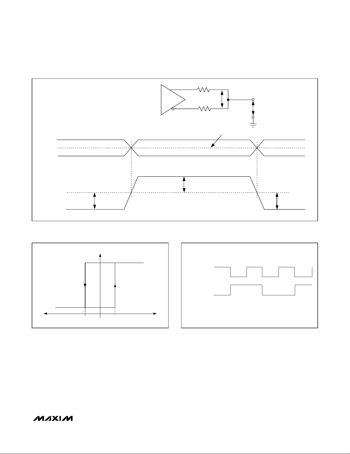
Figure 1. MAX9257 LVDS DC Output Parameters
Figure 2. Input Hysteresis
Figure 3. MAX9257 Worst-Case Pattern Input
SDO-
SDO+
(SDO+) - (SDO-)
(-) VOS(+)
V
OS
V
(-)
OD
/2
R
SDO+
SDO-
ΔV
OS
ΔVOD = |VOD(+) - VOD(-)|
L
/2
R
L
((SDO+) + (SDO-))/2
= |VOS(+) - VOS(-)|
VOD(+)
V
OD
V
OS
GND
V
(-)
OS
= 0V
V
OD
(-)
V
OD
-V
ID
V
HYST-
V
OUT
VID = 0V
V
HYST+
PCLK_IN
DIN
NOTE: PCLK_IN PROGRAMMED FOR RISING LATCH EDGE.
+V
ID
Page 14
MAX9257/MAX9258
14 ______________________________________________________________________________________
Fully Programmable Serializer/Deserializer
with UART/I2C Control Channel
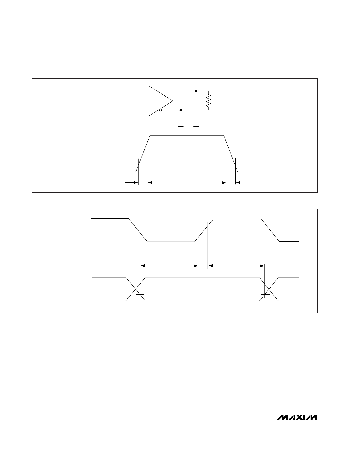
Figure 4. MAX9257 LVDS Control Channel Output Load and Output Rise/Fall Times
Figure 5. MAX9257 Input Setup and Hold Times
SDO+
R
L
SDO-
C
L
80%
(SDO+) - (SDO-)
t
RISE
PCLK_IN
V
ILMAX
t
SET
V
DIN, VSYNC_IN, HSYNC_IN
V
IHMIN
ILMAX
C
L
80%
20%20%
t
FALL
V
IHMIN
t
HOLD
V
IHMIN
V
ILMAX
NOTE: PCLK_IN PROGRAMMED FOR RISING LATCHING EDGE.
Page 15
MAX9257/MAX9258
______________________________________________________________________________________ 15
Fully Programmable Serializer/Deserializer
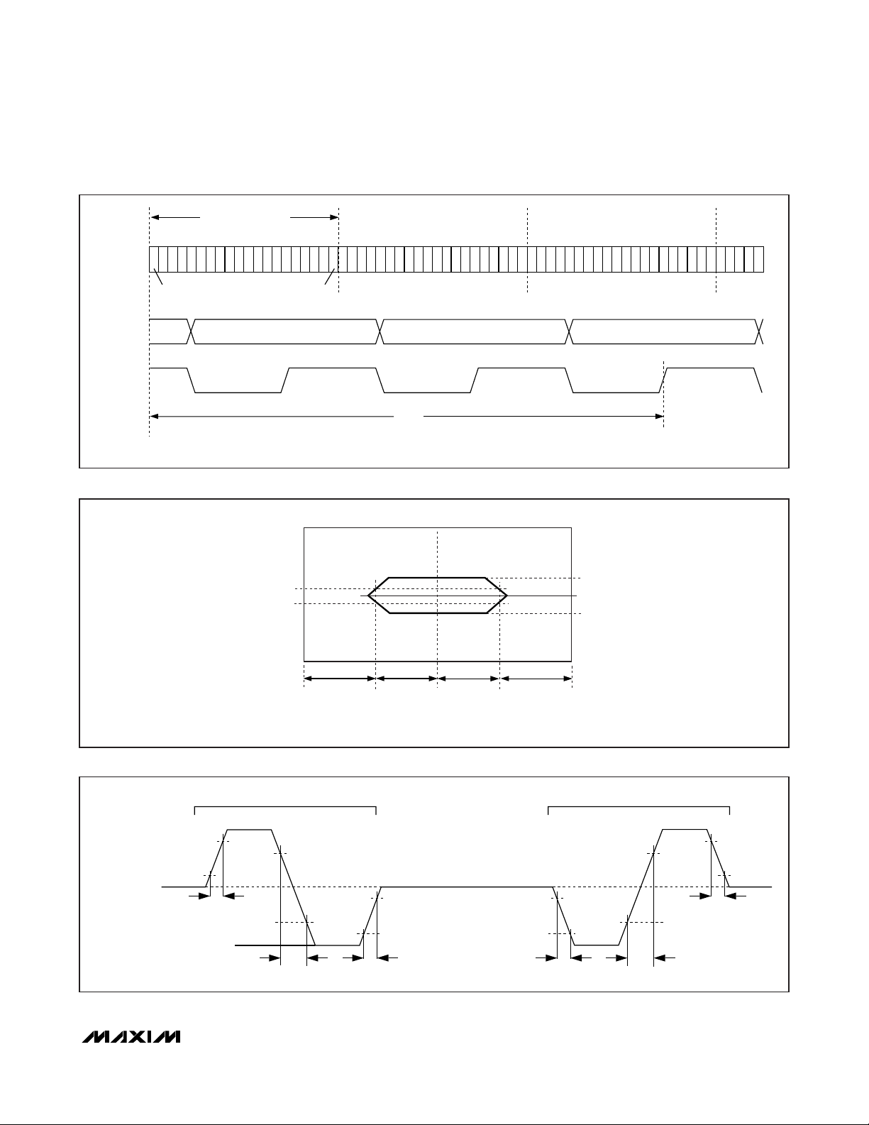
with UART/I2C Control Channel
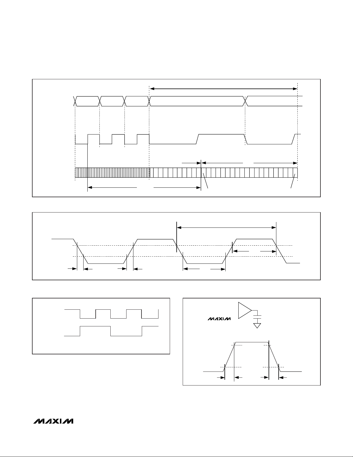
Figure 6. MAX9257 Parallel-to-Serial Delay
Figure 7. MAX9257 Parallel Input Clock Requirements
Figure 8. MAX9258 Worst-Case Pattern Output
Figure 9. MAX9258 Output Rise and Fall Times
DIN, HSYNC_IN,
VSYNC_IN
PCLK_IN
SDO
N
N+1
PCLK_IN
N+2
t
PSD1
N-1
EXPANDED TIME SCALE
N+3
N
FIRST BIT LAST BIT
t
T
t
HIGH
N+4
V
V
IHMIN
ILMAX
t
F
t
R
PCLK_OUT
DOUT
NOTE: PCLK_OUT PROGRAMMED FOR RISING LATCH EDGE.
t
LOW
C
L
MAX9258
SINGLE-ENDED OUTPUT LOAD
0.9 x V
CCOUT
0.1 x V
CCOUT
t
R
t
F
Page 16
MAX9257/MAX9258
16 ______________________________________________________________________________________
Fully Programmable Serializer/Deserializer
with UART/I2C Control Channel
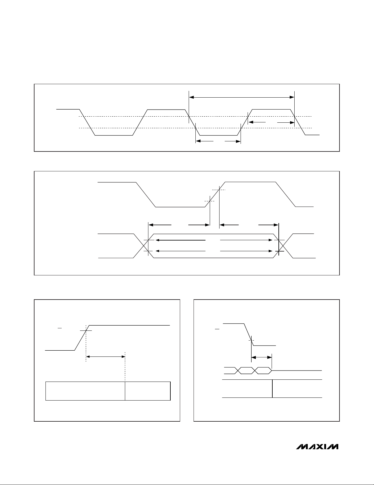
Figure 10. MAX9258 Clock Output High and Low Time
Figure 11. MAX9258 Output Data Valid Times
Figure 12. MAX9258 Power-Up Delay
Figure 13. MAX9258 Power-Down Delay
t
T
t
PCLK_OUT
t
LOW
HIGH
V
PCLK_OUT
V
OLMAX
OHMIN
V
OHMIN
V
OLMAX
DOUT, VSYNC_OUT,
HSYNC_OUT, LOCK
PD
POWERED DOWN
V
IHMIN
t
PUD
POWERED UP
(OUTPUTS ACTIVE)
t
DVB
V
OHMIN
V
OLMAX
NOTE: PCLK_OUT PROGRAMMED FOR RISING LATCHING EDGE.
PD
DOUT,
VSYNC,
HSYNC
V
ILMAX
t
DVA
t
PDD
HIGH IMPEDANCE
POWERED DOWNPOWERED UP
Page 17
MAX9257/MAX9258
______________________________________________________________________________________ 17
Fully Programmable Serializer/Deserializer
with UART/I2C Control Channel
Figure 14. MAX9258 Serial-to-Parallel Delay
Figure 15. MAX9258 Jitter Tolerance
Figure 16. Control Channel Transition Time
SERIAL-WORD LENGTH
SERIAL WORD N
SDI
SERIAL WORD N+1 SERIAL WORD N+2
LAST BIT
PARALLEL WORD N-2
DOUT,
HSYNC_OUT,
VSYNC_OUT
PCLK_OUT
FIRST BIT
NOTE: PCLK_OUT PROGRAMMED FOR RISING LATCHING EDGE.
+25mV
-25mV
PARALLEL WORD N-1 PARALLEL WORD N
t
SPD1
INPUT TEMPLATE FOR LVDS SERIAL
- V
V
SDI+
SDI-
+100mV
0V
-100mV
t
JT
t
S
t
S
t
JT
1.0UI0.75UI0.50UI0.25UI0.0UI
NOTE: UI IS ONE SERIAL BIT. TIME INPUT IS MEASURED DIFFERENTIALLY (V
1 0
0.8V
(SDO+) - (SDO-)
0.2V
OD(+)
0.2 x | V
OD(+)
t
R1A
+ V
OD(+)
0.8 x | V
| 0.2 x | V
OD(-)
t
F2
OD(+)
+ V
| 0.8 x | V
OD(-)
0.2V
OD(-)
0.8V
OD(-)
t
R1B
0.2V
0.8V
OD(-)
OD(-)
SDI+
- V
).
SDI-
0.8V
OD(+)
OD(+)
0.2V
OD(+)
t
F1B
+ V
|
OD(-)
+ V
OD(-)
|
t
R2
OD(+)
t
F1A
Page 18

MAX9257/MAX9258
Detailed Description
The MAX9257 serializer pairs with the MAX9258 deserializer to form a complete digital video serial link. The
electronic control unit (ECU) programs the registers in
the MAX9257, MAX9258, and peripheral devices, such
as a camera, during the control channel phase that
occurs at startup or during the vertical blanking time.
All control channel communication is half-duplex. The
UART communication between the MAX9258 and the
MAX9257 is encoded to allow transmission through ACcoupling capacitors. The MAX9257 communicates to
the peripheral device through UART or I2C.
The MAX9257/MAX9258 DC-balanced serializer and
deserializer operate from a 5MHz-to-70MHz parallel
clock frequency, and are capable of serializing and
deserializing programmable 10, 12, 14, 16, and 18 bits
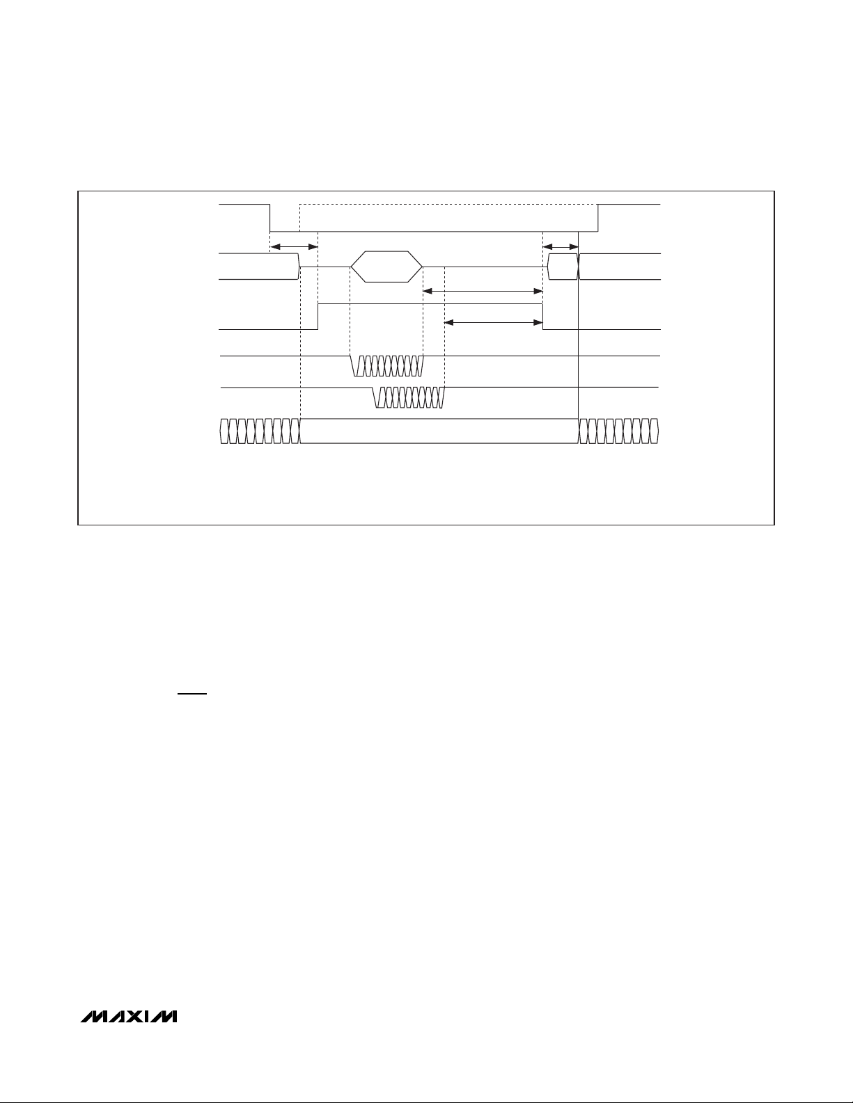
parallel data during the video phase. The MAX9257/
MAX9258 have two phases of operation: video and
control channel (Figures 19 and 20). During the video
phase, the MAX9257 accepts parallel video data and
transmits serial encoded data over the LVDS link. The
MAX9258 accepts the encoded serial LVDS data and
converts it back to parallel output data. The MAX9257
has dedicated inputs for HSYNC and VSYNC. The
selected VSYNC edge causes the MAX9257/MAX9258
to enter the control channel phase. Nonactive VSYNC
edge can be asserted after eight pixel clock cycles.
The video data are coded using two overhead bits
(EN0 and EN1) resulting in a serial-word length of N+2
bits. The MAX9257/MAX9258 feature programmable
18 ______________________________________________________________________________________
Fully Programmable Serializer/Deserializer
with UART/I2C Control Channel
Figure 17. Serial Link with I2C Camera Programming Interface (Base Mode)
Figure 18. Serial Link with UART Camera Programming Interface (Bypass Mode)
CAMERAECU
VIDEO DATA
MAX9258
MAX9257
VIDEO DATA
PIXEL CLOCK
HSYNC_OUT
VSYNC_OUT
PD
CCEN
ERROR
LOCK
RX
TX
DESERIALIZER
UARTUART
VIDEO DATA
PIXEL CLOCK
HSYNC_OUT
VSYNC_OUT
PD
CCEN
ERROR
LOCK
RX
TX
MAX9258
DESERIALIZER
UARTUART
PIXEL CLOCK
SERIALIZER
100Ω100Ω
UART-
2
C
TO-I
MAX9257
SERIALIZER
100Ω100Ω
UART
HSYNC_IN
VSYNC_IN
GPIO
SDA
SCL
VIDEO DATA
PIXEL CLOCK
HSYNC_IN
VSYNC_IN
GPIO
RX
TX
I2C
CAMERAECU
UART
Page 19

parity encoding that adds two parity bits to the serial
word. Bit 0 (EN0) is the LSB that is serialized first without parity enabled. The parity bits are serialized first
when parity is enabled.
The ECU programs the MAX9258, MAX9257, and
peripheral devices at startup and during the control
channel phase. In a digital video system, the control
channel phase occurs during the vertical blanking time
and synchronizes to the VSYNC signal. The programmable active edge of VSYNC initiates the control channel
phase. Nonactive edge of VSYNC can transition at any
time after 8 x t
T
if MAX9257 spread is not enabled and
0.5/f
SSM
when enabled. At the end of video phase, the
MAX9258 drives CCEN high to indicate to the ECU that
the control channel is open. Programmable timers and
ECU signal activity determine how long the control
channel stays open. The timers are reset by ECU signal
activity. ECU programming must not exceed the vertical
blanking time to avoid loss of video data.
After the control channel phase closes, the MAX9257
sends a 546 or 1090 word pattern as handshaking
(HSK) to synchronize the MAX9258’s internal clock
recovery circuit to the MAX9257’s transmitted data.
Following the handshaking, the control channel is
closed and the video phase begins. The serial LVDS
data is recovered and parallel data is valid on the programmed edge of the recovered pixel clock.
MAX9257/MAX9258
______________________________________________________________________________________ 19
Fully Programmable Serializer/Deserializer
with UART/I2C Control Channel
Figure 20. Video and Control Channel Phases (MAX9257 Spread is Enabled)
Figure 19. Video and Control Channel Phases (Spread Off)
8t
VSYNC_IN
SDI/O±
SDI/O±
T
VIDEO
CONTROL
HSK
VIDEO
CCEN
HSK = HANDSHAKING
0.5/f
SSM
VSYNC_IN
SDI/O±
SPREAD
PROFILE
SDI/O±
CCEN
VIDEO
(max)
CONTROL
HSK = HANDSHAKING
HSK
VIDEO
Page 20

MAX9257/MAX9258
20 ______________________________________________________________________________________
Fully Programmable Serializer/Deserializer
with UART/I2C Control Channel
Table 1. MAX9257 Power-Up Default Register Map (see the
MAX9257 Register Table
)
REGISTER NAME
REG0 0x00 0xB5
REG1 0x01 0x1F
REG2 0x02 0xA0
REG3 0x03 0xA0
REGISTER
ADDRESS (hex)
REG4 0x04
REG5 0x05 0xFA MAX9257 address = 1111 1010
REG6 0x06 0xFF End frame = 1111 1111
REG7 0x07 0xF8 MAX9258 address = 1111 1000
REG8 0x08 0x00
REG9 0x09 0x00
REG10 0x0A 0x00
POWER-UP VALUE
(hex)
1) REM = 0, 0x28
2) REM = 1, 0x30
PRATE = 10, 20MHz to 40MHz
SRATE = 11, 400Mbps to 840Mbps
PAREN = 0, parity disabled
PWIDTH = 101, parallel data width = 18
SPREAD = 000, spread = off
Reserved = 11111
STODIV = 1010, STO clock is pixel clock divided by 1024
STOCNT = 0000, STO counter counts to 1
ETODIV = 1010, ETO clock is pixel clock divided by 1024
ETOCNT = 0000, ETO counter counts to 1
VEDGE = 0, VSYNC active edge is falling
Reserved = 0
CKEDGE = 1, pixel clock active edge is rising
PD: 1) If REM = 0, PD = 0
2) If REM = 1, PD = 1
SEREN: 1) If REM = 0, SEREN = 1
2) If REM = 1, SEREN = 0
BYPFPLL = 0, filter PLL is active
Reserved = 0
PRBSEN = 0, PRBS test disabled
INTMODE = 0, interface with peripheral is UART
INTEN = 0, interface with peripheral is disabled
FAST = 0, UART bit rate = DC to 4.25Mbps
CTO = 000, never come back
BITRATE = 00, base mode bit rate = 95kbps to 400kbps
PRBSLEN = 0000, PRBS word length = 2
GPIO9DIR = 0, GPIO9 = input
GPIO8DIR = 0, GPIO8 = input
GPIO9 = 0
GPIO8 = 0
GPIO7DIR = 0, GPIO7 = input
GPIO6DIR = 0, GPIO6 = input
GPIO5DIR = 0, GPIO5 = input
GPIO4DIR = 0, GPIO4 = input
GPIO3DIR = 0, GPIO3 = input
GPIO2DIR = 0, GPIO2 = input
GPIO1DIR = 0, GPIO1 = input
GPIO0DIR = 0, GPIO0 = input
POWER-UP DEFAULT SETTINGS
21
Page 21

MAX9257/MAX9258
______________________________________________________________________________________ 21
Fully Programmable Serializer/Deserializer
with UART/I2C Control Channel
Table 1. MAX9257 Power-Up Default Register Map (continued)
Table 2. MAX9258 Power-Up Default Register Map (see the
MAX9258 Register Table
)
REGISTER NAME
REG11 0x0B 0x00
REG12 0x0C 0xE0
REG13 0x0D 0x00
REG14 0x0E 0x00
REGISTER
ADDRESS (hex)
REGISTER NAME
REG0 0x00 0xB5
REG1 0x01 0x00
REG2 0x02 0xA0
REG3 0x03 0xA0
REG4 0x04 0x20
REG5 0x05 0xF8 MAX9258 address = 1111 1000
REG6 0x06 0xFF End frame = 1111 1111
REG7 0x07 0x00
REGISTER
ADDRESS (hex)
POWER-UP VALUE
(hex)
POWER-UP VALUE
(hex)
POWER-UP DEFAULT SETTINGS
GPIO7 = 0
GPIO6 = 0
GPIO5 = 0
GPIO4 = 0
GPIO3 = 0
GPIO2 = 0
GPIO1 = 0
GPIO0 = 0
PREEMP = 111, preemphasis = 0%
Reserved = 00000
Reserved = 000000
I2CFILT = 00, I
1) 95kbps to 400kbps = 100ns
2) 400kbps to 1000kbps = 50ns
3) 1000kbps to 4250kbps = 10ns
Reserved = 0000 000
LOCKED = read only
2
C glitch filter settings:
POWER-UP DEFAULT SETTINGS
PRATE = 10, 20MHz to 40MHz
SRATE = 11, 400Mbps to 840Mbps
PAREN = 0, parity disabled
PWIDTH = 101, parallel data width = 18
SPREAD = 00, spread spectrum = off
AER = 0, error count is reset by reading error registers
Reserved = 0 0000
STODIV = 1010, STO clock is pixel clock divided by 1024
STOCNT = 0000, STO counter counts to 1
ETODIV = 1010, ETO clock is pixel clock divided by 1024
ETOCNT = 0000, ETO counter counts to 1
VEDGE = 0, VSYNC active edge is falling
HEDGE = 0, HSYNC active edge is falling
CKEDGE = 1, pixel clock active edge is rising
Reserved = 0000
PRBSEN = 0, PRBS test disabled
INTMODE = 0, interface with peripheral is UART
INTEN = 0, interface with peripheral is disabled
FAST = 0, UART bit rate = DC to 4.25Mbps
CTO = 000, never come back
BITRATE = 00, base mode bit rate = 95kbps to 400kbps
Page 22

MAX9257/MAX9258
Tables 1 and 2 show the default power-up values for
the MAX9257/MAX9258 registers. Tables 3 and 4 show
the input and output supply references.
Parallel-Word Width
The parallel-word width is made up of the video data
bits, HYSNC, and VSYNC. The video data bits are programmable from 8 to 16 depending on the pixel clock,
serial-data rate, and parity. Table 16 shows the parallelword width.
Serial-Word Length
The serial-word length is made up of the parallel-word
width, encoding bits, and parity bits. Tables 5–9 show
the serial video format and serial-word lengths without
parity. Tables 10–13 show with parity bits included.
LVDS Serial Data
Serial LVDS data is transmitted least significant bit (LSB)
to most significant bit (MSB) as shown in Tables 5
through 13. The ECU at startup can program the parallel
word width, serial frequency range, parity, spread-spectrum, and pixel clock frequency range
(
see the
MAX9257
Register Table
and the
MAX9258 Register Table)
.
22 ______________________________________________________________________________________
Fully Programmable Serializer/Deserializer
with UART/I2C Control Channel
Table 2. MAX9258 Power-Up Default Register Map (continued)
Table 3. MAX9257 I/O Supply
Table 4. MAX9258 I/O Supply
REGISTER NAME
REG8 0x08 0x10
REG9 0x09 0x00
REG10 0x0A 0x00 Parity errors video (8 LSBs) = read only
REG11 0x0B 0x00 Parity errors video (8 MSBs) = read only
REG12 0x0C 0x00 PRBS bit errors = read only
REG13 0x0D 0x00
REGISTER
ADDRESS (hex)
POWER-UP VALUE
(hex)
POWER-UP DEFAULT SETTINGS
PATHRLO = 0001 0000
parity threshold = 16
PATHRHI = 0000 0000,
parity threshold = 16
Reserved = 000
Parity error, communication with MAX9258 = read only
Frame error, communication with MAX9258 = read only
Parity error, communication with MAX9257 = read only
Frame error, communication with MAX9257 = read only
2
C error, communication with peripheral = read only
I
INPUTS/OUTPUTS SUPPLY
PCLK_IN, HSYNC_IN, VSYNC_IN,
DIN[0:7], DIN[8:15]/GPIO[0:7],
GPIO8, GPIO9
SDO+, SDO- V
SCL/TX, SDA/RX, REM V
V
CCIO
CCLVDS
CC
INPUTS/OUTPUTS SUPPLY
All inputs and outputs V
SDI+, SDI- V
CCOUT
CCLVDS
Page 23

MAX9257/MAX9258
______________________________________________________________________________________ 23
Fully Programmable Serializer/Deserializer
with UART/I2C Control Channel
Table 5. Serial Video Data Format for 20-Bit Serial-Word Length (Parallel-Word Width = 18)
Table 6. Serial Video Data Format for 18-Bit Serial-Word Length (Parallel-Word Width = 16)
Table 7. Serial Video Data Format for 16-Bit Serial-Word Length (Parallel-Word Width = 14)
Table 8. Serial Video Data Format for 14-Bit Serial-Word Length (Parallel-Word Width = 12)
Table 9. Serial Video Data Format for 12-Bit Serial-Word Length (Parallel-Word Width = 10)
Table 10. Format for 20-Bit Serial-Word Length with Parity (Parallel-Word Width = 16)
Table 11. Format for 18-Bit Serial-Word Length with Parity (Parallel-Word Width = 14)
Table 12. Format for 16-Bit Serial-Word Length with Parity (Parallel-Word Width = 12)
Table 13. Format for 14-Bit Serial-Word Length with Parity (Parallel-Word Width = 10)
BIT 1 2 3 4 567891011121314151617181920
NAME EN0 EN1 HSYNC VSYNC D0 D1 D2 D3 D4 D5 D6 D7 D8 D9 D10 D11 D12 D13 D14 D15
BIT 1 2 3 4 5 6 7 8 9 101112131415161718
NAME EN0 EN1 HSYNC VSYNC D0 D1 D2 D3 D4 D5 D6 D7 D8 D9 D10 D11 D12 D13
BIT 12 3 4 5678910111213141516
NAME EN0 EN1 HSYNC VSYNC D0 D1 D2 D3 D4 D5 D6 D7 D8 D9 D10 D11
BIT 1 2 3 4 5 6 7 8 9 10 11 12 13 14
NAME EN0 EN1 HSYNC VSYNC D0 D1 D2 D3 D4 D5 D6 D7 D8 D9
BIT 1234 5 6 7 8 9 101112
NAME EN0 EN1 HSYNC VSYNC D0 D1 D2 D3 D4 D5 D6 D7
BIT 1 2 3 4 5 6 7 8 9 10111213141516 17 18 19 20
NAME PR PRB EN0 EN1 HSYNC VSYNC D0 D1 D2 D3 D4 D5 D6 D7 D8 D9 D10 D11 D12 D13
BIT 1 2 3 4 5 6 7 8 9 10111213141516 17 18
NAME PR PRB EN0 EN1 HSYNC VSYNC D0 D1 D2 D3 D4 D5 D6 D7 D8 D9 D10 D11
BIT 1 2 3 4 5 6 7 8 9 10 11 12 13 14 15 16
NAME PR PRB EN0 EN1 HSYNC VSYNC D0 D1 D2 D3 D4 D5 D6 D7 D8 D9
BIT 1 2 3 4 5 6 7 8 9 10 11 12 13 14
NAME PR PRB EN0 EN1 HSYNC VSYNC D0 D1 D2 D3 D4 D5 D6 D7
Page 24

MAX9257/MAX9258
Pixel Clock Frequency Range
The MAX9257/MAX9258 each have registers that can
be configured at startup. Depending on the word
length, the MAX9257 multiplies PCLK_IN (pixel clock)
by 12, 14, 16, 18, or 20 using an internal PLL to generate the serial clock. Use Table 20 for proper selection
of available PCLK frequency and serial-data ranges.
Parallel data is serialized using the serial-clock and
serialized bits are transmitted at the MAX9257 LVDS
outputs. The MAX9257/MAX9258 support a wide range
for PCLK_IN (Table 14). If the pixel clock frequency
needs to change to a frequency outside the programmed range, the ECU must program both the
MAX9257 and the MAX9258 in the same control channel session.
Serial-Data Rate Range
The word length and pixel clock is limited by the maximum serial-data rate of 840Mbps. The following formula
shows the relation between word length, pixel clock,
and serial clock:
Serial-word length x pixel clock = serial-data rate
≤
840Mbps
For example, if PCLK_IN is 70MHz, the serial-word
length has to be 12 bits including DC balance bits if
parity is not enabled to keep the serial-data rate under
840Mbps. If the serial-word length is 20 bits, the maximum PCLK_IN frequency is 42MHz. The serial-data
rate can vary from 60Mbps to 840Mbps and can be
programmed at power-up (Table 15). Use Table 20 for
proper selection of available PCLK frequency and serial
data ranges. Operating in the incorrect range for either
the serial-data rate or PCLK_IN can result in excessive
current dissipation and failure of the MAX9258 to lock
to the MAX9257.
LVDS Common-Mode Bias
The output common-mode bias is 1.2V at the LVDS
inputs on the MAX9258 and LVDS outputs on the
MAX9257. No external resistors are required to provide
bias for AC-coupling the LVDS inputs and outputs.
LVDS Termination
Terminate the LVDS link at both ends with the characteristic impedance of the transmission line (typically
100Ω differential). The LVDS inputs and outputs are
high impedance to GND and differentially.
Spread-Spectrum Selection
The MAX9257/MAX9258 each have spread-spectrum
options. Both should not be turned on at the same time.
When the MAX9257 is programmed for spread spectrum,
the MAX9258 tracks and passes the spread to its clock
and data outputs. The MAX9257/MAX9258 are both
center spread (Figure 21). The control channel does
not use spread spectrum, but has slower transition
times.
MAX9258 Spread Spectrum
The MAX9258 features a programmable spread-spectrum clock and data outputs for reduced EMI. The single-ended data outputs are programmable for no
spread, ±2%, or ±4% (see the
Typical Operating
Characteristics
) around the recovered pixel clock frequency. The output spread is programmed in register
REG1[7:6]. Table 17 shows the spread options, and
Table 18 shows the various modulation rates.
MAX9257 Spread Spectrum
The MAX9257 features programmable spread spectrum
for the LVDS outputs. Table 19 shows various spread
options, and Table 20 shows the various modulation
rates. Only one device (the MAX9257 or the MAX9258)
should be programmed for spread spectrum at a time. If
the MAX9257 is programmed for spread, the MAX9258
24 ______________________________________________________________________________________
Fully Programmable Serializer/Deserializer
with UART/I2C Control Channel
Table 14. MAX9257 Pixel Clock Range
(PCLK_IN)
Table 15. Serial-Data Rate Range
Table 16. Parallel-Word Width
FREQUENCY (MHz) PRATE (REG0[7:6])
5–10 00
10–20 01
20–40 10
40–70 11
SERIAL-DATA RATE (Mbps) SRATE (REG0[5:4])
60–100 00
100–200 01
200–400 10
400–840 11
PARALLEL-WORD WIDTH PWIDTH (REG0[2:0])
10 000
12 001
14 010
16 011
18 1XX
Page 25

tracks and passes the spread to the data and clock outputs. The PRATE range of 00 and 01 (5MHz ≤ PCLK ≤
20MHz) supports all the spread options. The PRATE
range of 10 and 11 (20MHz ≤ PCLK ≤ 70MHz) requires
that the spread be 2% or less.
Pixel Clock Jitter Filter
The MAX9257 has a PLL to filter high-frequency pixel
clock jitter on PCLK_IN. The FPLL can be bypassed by
writing 1 to REG4[2]. The FPLL improves the
MAX9258’s data recovery by filtering out the high-frequency components from the pixel clock that the
MAX9258 cannot track. The 3db bandwidth of the FPLL
is 100kHz (typ).
LVDS Output Preemphasis (SDO±)
The MAX9257 features programmable preemphasis
where extra current is added when the LVDS outputs
transition on the serial link. Preemphasis provides additional current to the normal drive current. For example,
20% preemphasis provides 20% greater current than
the normal drive current. Current is boosted only on the
transitions and returns to the normal drive current after
switching. Select the preemphasis level to optimize the
eye diagram. Preemphasis boosts the high-frequency
content of the LVDS outputs to enable driving greater
cable lengths. The amount of preemphasis is programmed in REG12[7:5] (Table 21).
VSYNC, HSYNC, and Pixel Clock Polarity
PCLK: The MAX9257 is programmable to latch data on
either rising or falling edge of PCLK. The polarity of
PCLKOUT at the MAX9258 can be independent of the
MAX9257 PCLK active edge. The polarity of PCLK can
be programmed using REG4[5] of the MAX9257 and
the MAX9258.
VSYNC: The MAX9257 and the MAX9258 enter control
channel on the falling edge of VSYNC. The default register settings are VSYNC active falling edge for both the
MAX9257 and the MAX9258. If the VSYNC active edge
is programmed for rising edge at the MAX9257, the
MAX9258 VSYNC active edge must also be programmed for rising edge to reproduce VSYNC rising
edge at the MAX9258 output. However, matching the
polarity of the VSYNC active edge between the
MAX9257 and the MAX9258 is not a requirement for
proper operation.
HSYNC: HSYNC active-edge polarity is programmable
for the MAX9258.
General Purpose I/Os (GPIOs)
The MAX9257 has up to 10 GPIOs available. GPIO8
and GPIO9 are always available while GPIO[0:7] are
available depending on the parallel-word width (Table
22). If GPIOs are not available, the corresponding GPIO
bits are not used.
MAX9257/MAX9258
______________________________________________________________________________________ 25
Fully Programmable Serializer/Deserializer
with UART/I2C Control Channel
Figure 21. Simplified Modulation Profile for the MAX9257/MAX9258
Table 17. MAX9258 Spread
Table 18. MAX9258 Modulation Rate
Table 19. MAX9257 LVDS Output Spread
FREQUENCY
1/f
SSM
(MAX)
f
SPREAD
f
PCLK_IN
f
(MIN)
SPREAD
TIME
PRATE (REG1[7:6]) SPREAD (%)
00 Off
01 ±2
10 Off
11 ±4
PRATE
(REG1[7:6])
00 PCLK/312 16 to 32
01 PCLK/520 19.2 to 38.5
10 PCLK/1040 19.2 to 38.5
11 PCLK/1248 32 to 56
MODULATION RATE f
RANGE (kHz)
SSM
REG1[7:5] SPREAD (%)
000 Off
001 ±1.5
010 ±1.75
011 ±2
100 Off
101 ±3
110 ±3.5
111 ±4
Page 26

MAX9257/MAX9258
A GPIO can be programmed to drive an LVCMOS logic
level or to read a logic input. The register bit that sets
the output level when the GPIO is programmed as an
output stores the input level when the GPIO is programmed as an input.
Open-Drain Outputs (LOCK,
ERROR
)
LOCK and ERROR are open-drain outputs that require
a pullup resistor to an external supply. ERROR asserts
low when an error occurs and LOCK is high impedance
when the MAX9258 is locked to the MAX9257 and
remains high under the locked condition. When the
devices are in shutdown, the channel is not locked and
LOCK goes high impedance, is pulled high, and should
be ignored. ERROR is high impedance at shutdown
and remains high. In choosing pullup resistors, there is
a tradeoff between power dissipation and speed; 10kΩ
pullup should be sufficient.
26 ______________________________________________________________________________________
Fully Programmable Serializer/Deserializer
with UART/I2C Control Channel
Table 20. MAX9257 Modulation Rate
SERIAL-WORD
LENGTH
12
14
16
18
20
SRATE PRATE
11 11 40–70 PCLK/2728 14.7 to 25.7
11 10 33.3–40 PCLK/1736 19.2 to 23.0
10 10 20–33.3 PCLK/1612 12.4 to 20.7
10 01 16.6–20 PCLK/992 16.7 to 20.2
01 01 10–16.6 PCLK/1116 9.0 to 14.9
01 00 8.3–10 PCLK/744 11.2 to 13.4
00 00 5–8.3 PCLK/868 5.8 to 9.6
11 11 40–60 PCLK/2304 17.4 to 26.0
11 10 28.6–40 PCLK/1728 16.6 to 23.1
10 10 20–28.6 PCLK/1440 13.9 to 19.9
10 01 14.3–20 PCLK/1008 14.2 to 19.8
01 01 10–14.3 PCLK/1008 9.9 to 14.2
01 00 7.1–10 PCLK/720 9.9 to 13.9
00 00 5–7.1 PCLK/720 6.9 to 9.9
11 11 40–52.5 PCLK/1968 20.3 to 26.7
11 10 25–40 PCLK/1640 15.2 to 24.4
10 10 20–25 PCLK/1312 15.2 to 19.1
10 01 12.5–20 PCLK/984 12.7 to 20.3
01 01 10–12.5 PCLK/820 12.2 to 15.2
01 00 6.25–10 PCLK/656 9.5 to 15.2
00 00 5–6.25 PCLK/656 7.6 to 9.5
11 11 40–46.6 PCLK/1840 21.7 to 25.3
11 10 22.2–40 PCLK/1472 15.1 to 27.2
10 10 20–22.2 PCLK/1104 18.1 to 20.1
10 01 11.1–20 PCLK/920 12.1 to 21.7
01 01 10–11.1 PCLK/736 13.6 to 15.1
01 00 5.6–10 PCLK/736 7.6 to 13.6
00 00 5–5.6 PCLK/552 9.1 to 10.1
11 11 40–42 PCLK/1632 24.5 to 25.7
11 10 20–40 PCLK/1632 12.3 to 24.5
10 01 10–20 PCLK/1020 9.8 to 19.6
01 00 5–10 PCLK/816 6.1 to 12.3
PCLK RANGE
(MHz)
MODULATION RATE f
RANGE (kHz)
SSM
Page 27

The LOCK and ERROR outputs can be wired in an
AND configuration if you have multiple serializers and
deserializers, or a single serializer fanned out to multiple deserializers through a repeater. For such situations, wire the multiple LOCK outputs together and use
a single pullup resistor to pull up all the lines high.
LOCK is high if all the devices are locked. Do the same
thing for ERROR; ERROR is low if any MAX9258 reports
errors.
Base Mode and Bypass Mode (Basics)
In the control channel phase, there are two modes: base
and bypass. In base mode, ECU always communicates
using the MAX9257/MAX9258 UART protocol and communication with a peripheral device is performed in I2C
by the MAX9257. Packets not addressed to the
MAX9257 or the MAX9258 get converted to I2C and
passed to the peripheral device. Similarly, I2C packets
from the peripheral device get converted to UART packets in the reverse direction. ECU can disable communication to the peripheral device by writing a 0 to INTEN
(REG8[6] in the MAX9257 and REG7[6] in the MAX9258).
Base mode is the default mode. Bypass mode is entered
by writing a 0 to INTMODE and 1 to INTEN (Table 23).
Bypass mode is exited if there is no activity from ECU in
the control channel for the duration of CTO. When CTO
times out, INTEN reverts back to 0 and MAX9257/
MAX9258 revert back to base mode. To permanently
stay in bypass mode, ECU can lock the CTO timer or
program CTO to be longer than ETO and STO.
Timers
The MAX9257/MAX9258 feature three different timers.
The start timeout (STO) and end timeout (ETO) control
the duration of the control channel. The come-back
timeout (CTO) controls the duration of bypass mode.
STO Timer
The STO (start timeout) timer closes the control channel if
the ECU does not start using the control channel within
the STO timeout period. The STO timer is configured by
MAX9257/MAX9258
______________________________________________________________________________________ 27
Fully Programmable Serializer/Deserializer
with UART/I2C Control Channel
Table 21. Preemphasis
Table 22. GPIOs vs. Parallel-Word Width
Table 23. Selection of Base Mode or
Bypass Mode
Table 24. STO Clock Divide Ratio
REG12[7:5] PREEMPHASIS (%)
000,101,110 20
001 40
010 60
011 80
100 100
111 0
PARALLEL-WORD
WIDTH (N)
18 GPIO[8:9]
16 GPIO[6:9]
14 GPIO[4:9]
12 GPIO[2:9]
10 GPIO[0:9]
GPIOs AVAILABLE
INTEN
MAX9257 REG8[6],
MAX9258 REG7[6]
0X
11
10
INTMODE
MAX9257 REG8[7],
MAX9258 REG7[7]
MODE
Base mode,
communication
with peripheral is
not enabled
Base mode,
communication
with peripheral is
enabled (I
Bypass mode,
communication
with MAX9257/
MAX9258 is not
enabled,
communication
with peripheral is
enabled (UART)
2
C)
REG2[7:4] STODIV
00XX 16
0100 16
0101 32
0110 64
0111 128
1000 256
1001 512
1010 1024
1011 2048
1100 4096
1101 8192
1110 16,384
1111 32,768
Page 28

MAX9257/MAX9258
register REG2 for both the MAX9257 and the MAX9258.
The four bits of REG2[7:4] select the divide ratio (STODIV)
for the STO clock as a function of the pixel clock (Table
24). The timeout period is determined by counter bits
REG2[3:0] that increment once every STO clock period.
Write to REG2[3:0] to determine the counter end time.
The STO counter counts to the programmed STOCNT +
1. The ECU must begin communicating before STO times
out, otherwise, the control channel closes (Figure 22). The
STO timeout period is given by:
For example:
If the pixel clock frequency is set to 16MHz, STODIV is
set to 1010 (STODIV = 1024), and STOCNT is set to
1001 (STOCNT = 9), the STO timer counts with
15.625kHz STO clock (16MHz/1024) internally until it
reaches 10 and timer expires. The t
STO
is equal to tTx
1024 x 10 = 640µs.
The default value for STODIV is 1024 while the default
value for STOCNT is 0. That means the STO timeout
period is equal 1024 pixel clock cycles. Activity from
the ECU on the control channel shuts off the STO timer
and starts the ETO timer.
ETO Timer
The ETO (end timeout) timer closes the control channel
if the ECU stops communicating for the ETO timeout
period. Configure register REG3[7:4] for both the
MAX9257 and the MAX9258 to select the divide ratio
(ETODIV) for the ETO clock as a function of the pixel
clock (Table 25). The timeout period is determined by
28 ______________________________________________________________________________________
Fully Programmable Serializer/Deserializer
with UART/I2C Control Channel
Table 25. ETO Clock Divide Ratio
Figure 22. Control Channel Closing Due to STO Timeout
VSYNC_IN
T1
SDI/O±
CCEN
TX
RX
DOUT_
T1 = TIME TO ENTER CONTROL CHANNEL
T2 = STO TIMEOUT PERIOD
T3 = CONTROL CHANNEL EXIT TIME DUE TO STO
HSK = HANDSHAKING BETWEEN THE MAX9257 AND THE MAX9258
VIDEO
⎛
⎞
t
STO
1
=
⎜
f
⎝
CLK
STODIV STOCNT
×× +
⎟
⎠
1()
T2
FROZEN
REG3[7:4] ETODIV
00XX 16
0100 16
0101 32
0110 64
0111 128
1000 256
1001 512
1010 1024
1011 2048
1100 4096
1101 8192
1110 16,384
1111 32,768
T3
HSK
VIDEO
Page 29
counter bits REG3[3:0] that increment once every ETO
clock period. Write to REG3[3:0] to determine the
counter end time. The ETO counter counts to the programmed ETOCNT + 1. Any ECU activity resets the
ETO timer. When the ECU stops transmitting data for
the ETO timeout period, the control channel closes
(Figure 23).
For example:
If the pixel clock frequency is set to 16MHz, ETODIV is
set to 1010 (ETODIV = 1024), and ETOCNT is set to
1001 (ETOCNT = 9), the ETO timer counts with the
15.625kHz ETO clock (16MHz/1024) internally until it
reaches 10 and timer expires. The t
ETO
is equal to tTx
1024 x 10 = 640µs.
The default value for ETODIV is 1024 while the default
value for ETOCNT is 0. That means the ETO timeout
period is equal to 1,024 pixel clock cycles.
Closing the Control Channel
After the MAX9257 detects the active VSYNC edge, it
sends three synchronization words. Once the MAX9258
sees the active VSYNC transition and detects three synchronization words, it enters the control channel phase
and CCEN goes high. There is a brief delay of T1
between the VSYNC transition and CCEN transitioning
high. The ECU is allowed to communicate when CCEN
is high.
If the ECU does not communicate while CCEN is high
(Figure 22), the link remains silent and STO starts
counting towards its preset timeout counter value. If
STO times out (T2), CCEN transitions low and the control channel closes.
If the ECU communicates while CCEN is high and
before STO expires (Figure 23), the STO timer is turned
off and ETO timer is enabled. The ETO counter (ETOCNT+1) is reset to 0 whenever activity from ECU (base
mode) or ECU and Camera (bypass mode) is detected.
As long as there is activity from ECU (base mode) or
ECU and Camera (bypass mode) on the link, the channel does not close and the ETO counter resets. After
the ECU (base mode) or ECU and Camera (bypass
mode) ceases link activity, ETO times out (T4), CCEN
transitions low, and the control channel closes.
Another way to close the control channel in base mode
is for the ECU to send an end frame (EF) to close the
control channel without waiting for ETO to time out.
Whenever EF is received by both the MAX9257/
MAX9258, control channel closes immediately and
CCEN goes low. A synchronization frame must precede
EF. End frame cannot be used in bypass mode. The
control channel must close by EF to report errors back
to the ECU.
MAX9257/MAX9258
______________________________________________________________________________________ 29
Fully Programmable Serializer/Deserializer
with UART/I2C Control Channel
Figure 23. Control Channel Closing Due to ETO Timeout
VSYNC_IN
T1
SDI/O±
CCEN
TX
RX
DOUT_
T1 = TIME TO ENTER CONTROL CHANNEL
T4 = ETO TIMEOUT PERIOD
T5 = CONTROL CHANNEL EXIT TIME DUE TO ETO
HSK = HANDSHAKING BETWEEN MAX9257 AND MAX9258
VIDEO
ECU
ACTIVITY
⎛
⎞
t
ETO
1
=
⎜
f
⎝
CLK
ETODIV ETOCNT
×× +
⎟
⎠
1()
T5
HSK
T4 (BASE MODE)
T4 (BYPASS MODE)
FROZEN
VIDEO
Page 30

MAX9257/MAX9258
After the control channel closes, there is a brief handshake period (T3 in Figure 22 and T5 in Figure 23)
between the MAX9257 and the MAX9258. The
MAX9258 sends a special lock frame to the MAX9257
to indicate if PLL is still locked. The MAX9258 sends the
lock frame if the number of decoding errors didn’t
exceed a threshold in the last LVDS video phase session. The MAX9258 features a proprietary VCO lock
that prevents frequency drift while in the control channel for extended periods of time. If MAX9257 receives
the lock frame, it understands that the MAX9258 is in a
locked state and sends a short training sequence. If the
lock frame is not received by the MAX9257, it assumes
that the MAX9258 is not locked and sends a long training sequence. After the short or long training sequence
is complete, the MAX9257 sends three special synchronization words before entering the video phase.
Training sequence is used to resynchronize the
MAX9257/MAX9258 before the video phase starts.
The MAX9257/MAX9258 control channel duration is
independent of VSYNC. The control channel does not
close when VSYNC deasserts, which allows the use of
a VSYNC interrupt signal on VSYNC_IN. The control
channel must be closed by STO, ETO, or EF. If the control channel does not close before video data becomes
available, video data can be lost.
STO/ETO Timer Programming
STO and ETO can be programmed given the values of
T2, T4, and maximum values of T1, T3, and T5 (Figures
22, 23):
tT= pixel clock period, t
UCLK
= UART period
When spread spectrum is not enabled in MAX9257:
max(T1) = 2.5µs + (3 x tT) + (4 x t
UCLK
)
When spread spectrum is enabled in MAX9257:
max(T1) = 2.5µs + (1400 x tT) + (4 x t
UCLK
)
T2 = t
STO
T4 = t
ETO
When pixel clock frequency range (PRATE) is 00 or 01:
When pixel clock frequency range (PRATE) is 10 or 11:
CTO Timer
The CTO (come-back timeout) timer temporarily or permanently blocks programming to the MAX9257/
MAX9258 registers. CTO keeps the MAX9257/ MAX9258
in bypass mode for the CTO timeout period (Table 26).
Bypass mode can only be exited when the CTO timer
expires. The CTO timer uses the UART bit times for its
counter. Note that STO and ETO timers use the pixel
clock while CTO uses the UART bit times. The UART
period t
UCLK
synchronizes with the UART bit times,
which synchronize every time the SYNC frame is sent.
When the CTO timer times out, INTEN bit in both
devices is set to 0 and the MAX9257/MAX9258 revert
back to base mode. If communication with the
MAX9257/MAX9258 is not needed after initial programming is complete, CTO may be set to 000 (never come
back). In this case, CTO never expires and the
MAX9257/MAX9258 stay in bypass mode until they are
powered down. This prevents accidental programming
of the MAX9257/MAX9258 while ECU communicates
with the peripheral using a different UART protocol from
the MAX9257/MAX9258 UART protocol.
The overall CTO timeout is calculated as follows:
t
CTO
= t
UCLK
x CTO
30 ______________________________________________________________________________________
Fully Programmable Serializer/Deserializer
with UART/I2C Control Channel
Table 26. CTO Counter Timeout Period
⎛
t
⎛
max( ) ) ( )
T
3
max( ) ) ( )
T
5
STO
=
⎜
⎜
⎝
8
⎝
⎛
t
⎛
ETO
=
⎜
⎜
⎝
8
⎝
⎞
⎞
546 20
×+ ×
+
⎟
⎟
⎠
⎠
⎞
⎞
⎟
⎠
×+ ×
+
546 20
⎟
⎠
tt
T UCLK
tt
T UCLK
MAX9257 REG2[7:4]
MAX9258 REG3[7:4]
000
001 16
010 32
011 48
100 64
101 80
110 96
111 112
⎛
t
⎛
max( ) ) ( )
T
3
max( ) ) ( )
T
5
STO
=
⎜
⎜
⎝
8
⎝
⎛
t
⎛
ETO
=
⎜
⎜
⎝
8
⎝
COUNTER USING UART BIT
TIMES
Never come back
(lockout)
⎞
1090 20
+
1090 20
+
tt
×+ ×
TUCLK
⎟
⎠
⎞
tt
×+ ×
TUCLK
⎟
⎠
⎞
⎟
⎠
⎞
⎟
⎠
Page 31

Assuming a UART bit rate of 2Mbps, REG2[7:4],
REG3[7:4] = 100 (Table 26), CTO = 64, CTO timeout
calculated as:
t
CTO
= (0.5µs) × 64 = 32µs
Link Power-Up
The MAX9258 powers up when the power-down input
PD goes high. After approximately 130µs, CCEN goes
high, indicating the control channel is available. This
delay is required because the analog circuitry has to
fully wake up. There are two ways to power up the
MAX9257. The MAX9257 powers up according to the
state of REM. ECU powers up MAX9257 remotely (ECU
sends command to power up) when REM is pulled to
VCC. The MAX9257 powers up according to the supply
voltage when REM is grounded.
Powering the MAX9257 with Serialization Enabled
(REM = Ground at Power-Up)
When REM is grounded, the MAX9257 fully powers up
when power is applied. The power-down bit PD
(REG4[4]) is disabled and serialization bit SEREN
(REG4[3]) is enabled. If PCLK_IN is not running, the
MAX9257 stays in the control channel. After PCLK_IN is
applied, the control channel times out due to STO, ETO,
or EF. The MAX9257 starts the handshaking after the
MAX9257 locks to PCLK after 32,768 clock cycles. If
PCLK_IN is running, serialization starts automatically
after PLL of the MAX9257 locks to PCLK_IN with default
values in the registers.
Remote Power-Up of the MAX9257
(REM = Pulled Up to VCC)
When REM is pulled up to VCC, the MAX9257 wakes up
in a low power state, drawing less than 100µA supply
current. To wake-up the MAX9257, the ECU first transmits a dummy frame 0xDB and then waits at least
100µs to allow the MAX9257’s internal analog circuitry
to fully power up. Then the ECU configures the
MAX9257 registers, including a write to disable the PD
bit (REG4[4]) so that the MAX9257 does not return
back to the low power state. Every packet needs to
start with a synchronization frame (see the
UART
section). If the PD bit is not disabled within 70ms after
transmitting the dummy frame, the MAX9257 returns to
the low power state and the whole power-up sequence
needs to be repeated. After configuration is complete,
the ECU also needs to enable the SEREN bit to start the
video phase.
At initial power-up with REM pulled to VCC, default value
of SEREN bit is 0, so STO and ETO timers are not active.
Control channel is enabled as long as SEREN is 0.
This allows the control channel to be used for extensive
programming at initial power-up without the channel
timing out. UART, parity, framing and packet errors in
the control channel communications are reported if end
frame is used to close control channel (see the
MAX9258 Error Checking and Reporting
section). For
faster identification of errors, verify every write command by reading back the registers before enabling
serialization.
Link Power-Down
When the control channel is open, the ECU writes to the
PD bit to power down the MAX9257. In this case, to
power up the MAX9257 again, the power-up sequence
explained in the
Remote Power-Up of the MAX9257 (REM
= Pulled Up to VCC)
section needs to be repeated. The
MAX9258 has a PD input that powers down the device.
MAX9258 Error Checking and Reporting
The MAX9258 has an open-drain ERROR output. This
output indicates various error conditions encountered
during the operation of the system. When an error condition is detected and needs to be reported, ERROR
asserts low. ERROR indicates three error conditions:
UART, video parity, and PRBS errors.
UART Errors
During control channel communication in base mode,
the MAX9257/MAX9258 record UART frame, parity, and
packet errors. I2C errors are also recorded by
MAX9257 when I2C interface is enabled. If ECU closes
the control channel by using end frame (EF), the
MAX9257 sends a special internal UART frame back to
the MAX9258 called error frame. The MAX9257 UART
and I2C errors are reset at the next control channel. The
MAX9258 receives the error frame and records the
error status in its UART error register (REG13). ECU
must use end frame to the close control channel for the
MAX9257 to report back UART and I2C errors to the
MAX9258. Whenever one of the bits in the UART error
register is 1, ERROR asserts low. The UART error register is reset when ECU reads it, and ERROR deasserts
high immediately if UART errors were the only reason
that ERROR was asserted low. If the MAX9258 is not
locked (LOCK = low), UART error is not reported.
Video Parity Errors
When video parity check is enabled (REG0[3] in both
devices), the MAX9258 counts the number of video parity errors by checking recovered video words. Value of
this counter is reflected in PAERRHI (8 MSB bits,
REG11) and PAERRLO (8 LSB bits, REG10). If the number of detected parity errors is greater than or equal to
the parity error threshold PATHRHI (REG9) and
PATHRLO (REG8), then ERROR asserts low. In this
MAX9257/MAX9258
______________________________________________________________________________________ 31
Fully Programmable Serializer/Deserializer
with UART/I2C Control Channel
Page 32
MAX9257/MAX9258
case, ERROR deasserts high after next video phase
starts if video parity errors were the only reason that
ERROR was asserted low. To report parity errors in
bypass mode, program autoerror reset (AER) to 1
(REG1[5] = 1).
Autoerror Reset
The default method to reset errors is to read the respective error registers in the MAX9258 (registers 10, 11, and
13). If errors were present before the next control channel, the error count gets incremented to the previous
number. By setting the autoerror reset (AER) bit to 1, the
error registers reset when the control channel ends.
Setting AER to 1 does not reset PRBS errors.
PRBS Errors
During the PRBS test, the MAX9258 checks received
PRBS data words by comparing them to internally generated PRBS data. Detected errors are counted in the PRBS
error register (REG12) in the MAX9258. Whenever the
number of detected PRBS errors is more than 0, ERROR
asserts low. The PRBS error register is reset when ECU
writes a 0 to PRBSEN register (REG4[0]). In this case,
ERROR deasserts high immediately if PRBS errors were
the only reason that ERROR was asserted low.
Short Synchronization Pattern
The short synchronization pattern is part of the handshaking procedure between the MAX9257 and MAX9258 after
the control channel phase. It is used to resynchronize the
MAX9258’s clock and data recovery circuit to the
MAX9257 before the video phase begins. The MAX9257
transmits the short synchronization pattern when it
receives the lock frame from the MAX9258. The length of
short synchronization pattern is dependant on the PRATE
range. When PRATE is 00 or 01, the short synchronization pattern consists of 546 words and when PRATE is 10
or 11, the short synchronization pattern consists of 1090
words. Every word is one pixel clock period.
Long Synchronization Pattern
At power-up or when the MAX9257 does not receive a
lock frame from the MAX9258, the MAX9257 transmits a
long synchronization pattern. The long synchronization
pattern consists of 17,410 words. Every word is one
pixel clock period. When REM is high, if synchronization is not achieved after 62 attempts, the MAX9257
resets SEREN to 0 so that the control channel stays
open to allow troubleshooting. When REM is low, the
MAX9257/MAX9258 continuously tries to reestablish the
connection.
Lock Verification (Handshaking)
At the end of every vertical blanking time, the MAX9257
verifies that the MAX9258 did not lose lock. The
MAX9258 handshakes with the MAX9257 to indicate
lock status. The handshaking occurs after the channel
closes (Figures 22 and 23). If the number of decoding
errors in a time window did not exceed a certain threshold during the last video phase, the MAX9258 sends
back the lock frame that indicates lock. If the MAX9257
receives the lock frame, the MAX9257 transmits a short
synchronization pattern. The MAX9258 features a proprietary VCO mechanism that prevents frequency drift
while in the control channel. This allows for successful
resynchronization after extended use of control channel. If the number of decoding errors in a time window
exceeds a certain threshold, the MAX9258 loses lock,
LOCK goes low, and the lock frame is not sent. The
MAX9258 also loses lock if handshaking is not successful. If the MAX9257 does not receive the lock
frame, it transmits a long synchronization pattern before
the start of next video phase. When REM = 1, if the lock
frame is not received by the MAX9257 after 62 consecutive attempts to synchronize, SEREN is disabled so
that the control channel opens permanently for troubleshooting.
Link Status (LOCK and CCEN)
The LOCK output indicates whether the MAX9258 is
locked to the MAX9257. LOCK is an open-drain output
that needs to be pulled up to V
CC
. LOCK asserts low to
indicate that the MAX9258 is not locked to the
MAX9257 and high when it is. In the control channel
phase, LOCK stays high if LOCK is high in the video
phase. While in the control channel phase, the
MAX9258 PLL frequency is held constant, PCLK output
is active and data outputs are frozen at their last valid
value before entering the control channel. CCEN output
indicates whether the MAX9257/MAX9258 are in the
control channel phase or video phase. CCEN goes high
when the MAX9257/MAX9258 are in the control channel
phase (Table 27). Only at initial power-up, CCEN goes
high before communication in the control channel is
ready (see the
Link Power-Up
section).
32 ______________________________________________________________________________________
Fully Programmable Serializer/Deserializer
with UART/I2C Control Channel
Table 27. Link Status
LOCK CCEN INDICATION
1 0 LVDS channel active
1 1 Control channel active
0 X PLL loss of lock
Page 33

Control Channel
Overview of Control Channel Operation
The control channel is used by the ECU to program
registers in the MAX9257, MAX9258, and peripheral
devices (such as a camera) during vertical blanking,
after power-up, or when serialization is disabled.
Control channel communication is half-duplex UART.
The peripheral interface on the MAX9257 can be programmed to be I2C or UART. Operation of the control
channel is synchronized with the VSYNC input after the
ECU starts serialization of video data. Programmable
timers, ECU signal activity, and end frame determine
how long the control channel stays open. The control
channel remains open as long as there is signal activity
from the ECU. When the control channel closes, the
LVDS serial link is reestablished. Once serialization is
enabled, the programming of registers (including the
control channel overhead time) must be completed
within the vertical blanking time to avoid loss of video
data. VSYNC can deassert while control channel
remains open after eight pixel clock cycles.
The control channel phase begins on the transition of
the programmed active edge of VSYNC_IN. In video
applications, the VSYNC signal of the peripheral device
is connected to VSYNC_IN on the MAX9257. In other
applications, a different signal can be used to trigger
the control channel phase. When the MAX9257/
MAX9258 detect the VSYNC_IN transition, the LVDS
video phase disables and the control channel phase is
enabled.
The control channel operates in two modes: base and
bypass. In base mode, the ECU issues UART commands in a specified format to program the
MAX9257/MAX9258 registers. GPIO on the MAX9257
are also programmed in base mode. UART commands
are translated to I2C and output to peripheral devices
connected to the MAX9257 when not addressed to
either the MAX9257 or the MAX9258.
In bypass mode, programming of the MAX9257/
MAX9258 registers are temporarily or permanently
blocked depending on the programmed value of CTO.
Blocking prevents unintentional programming of the
MAX9257/MAX9258 registers when the ECU communicates with the peripheral using a UART protocol different than the one specified to program the MAX9257/
MAX9258. When the control channel is open, the
MAX9258 continues outputting the pixel clock while
HSYNC and video data are held at the last value. If
spread is enabled on the MAX9258, the pixel clock is
spread.
Control Channel Overhead
Control channel overhead consists of lock frame, short
synchronization sequence, and error frame. The lock
frame is transmitted between the MAX9257 and the
MAX9258 without action by the ECU. The error frame is
only sent in response to end frame. When MAX9257
spread spectrum is enabled, the control channel is
entered after spread reaches center frequency. The overhead from VSYNC falling edge to control channel enable
accounts for a maximum of 1400 pixel clock cycles.
Base Mode (Details)
Base mode allows the ECU to communicate with the
MAX9257/MAX9258 in UART and a peripheral device in
I2C. UART programming of the peripheral device is not
possible in base mode. UART packets from the ECU
need to follow a certain protocol to program the
MAX9257 and the MAX9258 (Figures 28 and 29).
Packets not addressed to the MAX9257/MAX9258 get
converted to I2C by the MAX9257 and pass to the
peripheral device. The MAX9257 receives I
2
C packets
from the peripheral device and converts them to UART
packets to send back to the ECU. To disable communication to the peripheral device, write a 0 to INTEN
(REG8[6] in the MAX9257 and REG7[6] in the MAX9258.
In base mode, the STO/ETO timers and the EF command
are used to control the duration of the control channel.
STO and ETO count up and expire when they reach their
programmed value. STO and ETO are not enabled at the
same time. STO is enabled after CCEN goes high. If there
is activity from the ECU before STO times out, STO is disabled and ETO is enabled. The ECU must begin a transaction within an STO timeout or else the channel closes.
The ECU can close the channel by allowing ETO to timeout. Activity from the ECU resets the ETO timer. Another
way to close the control channel is by sending an end
frame (EF). EF closes the channel within 2 to 3 bit times
after being received by the MAX9257/MAX9258. The
default value of EF is 0xFF, but can be programmed to
any other value besides the MAX9257 and the MAX9258
device addresses. The control channel must be closed
with EF for control channel errors to be reported.
Program STO to be longer than the time the ECU takes
to respond to opening of channel. Program ETO to be
longer than the time the ECU pauses between transactions. As long as the ECU performs transactions, ETO is
reset and the channel stays open.
The ECU must wait 14 or more bit times before addressing another device during the same control channel session. Failure to wait 14 bit times may result in the packet
boundary not being reset. Internal handshaking operations are automatically performed after the channel is
closed and before the video phase begins.
MAX9257/MAX9258
______________________________________________________________________________________ 33
Fully Programmable Serializer/Deserializer
with UART/I2C Control Channel
Page 34

MAX9257/MAX9258
UART-to-I2C Converter
The UART-to-I2C converter accepts UART read or write
packets issued by the ECU and converts them to an I2C
master protocol when in base mode. A slave can use an
ACK or NACK to indicate a busy or wait state, but cannot
hold SCL low to indicate a wait state. Multiple slaves are
supported. The UART-to-I2C conversion delay is less
than 22 UART bit times and needs to be taken into
account when setting the ETO and STO timeout periods
for read commands. UART-to-I2C converter converts
standard UART format to standard I2C format (Figure
25). This includes data-bit ordering conversion because
UART transmits the LSB in first while I2C transmits the
MSB first. UART/I2C read delay is a maximum 34 bit
times when reading from an I2C peripheral.
The MAX9257/MAX9258 store their own 7-bit device
addresses in register REG5. All packets not addressed
to the MAX9257/MAX9258 are forwarded to the UARTto-I2C converter. The I2C interfaces (SDA and SCL) are
open drain and actively drive a low state. When idle,
SDA and SCL are high impedance and pulled high by a
pullup resistor. SDA and SCL are idle when packets are
addressed to the MAX9257 or MAX9258. SDA and SCL
are also idle when the I2C interface is programmed to
be disabled.
Bypass Mode (Details)
In bypass mode, ECU activity and UART communication from the camera reset the ETO and CTO timers.
This allows the control channel to stay in bypass as
long as there is camera activity. In base mode, only
ECU activity resets the ETO and CTO timers.
Bypass mode temporarily or permanently blocks programming of the MAX9257/MAX9258. Bypass mode
allows only UART programming of peripheral device by
ECU. There is no I
2
C connection in bypass mode. Bypass
mode is entered by writing a 0 to INTMODE and by writing a 1 to INTEN (Table 23). Bypass mode disables ECU
programming of the MAX9257/MAX9258 to allow any
UART communication protocol with the peripheral device.
Once bypass mode is entered, the MAX9257/MAX9258
stay in bypass mode until CTO times out.
In bypass mode, the STO and ETO timers determine
the control channel duration. CTO timer determines
whether to revert back to base mode or not, and EF is
not recognized.
A useful setting in bypass mode is to set STO > CTO >
ETO because this setting is an alternative to permanent
bypass (Figure 24). Use this setting to stay in bypass
mode to avoid the overhead of entering from base mode
every time the control channel opens. If the ECU uses the
channel within a CTO timeout, ETO is activated and then
ETO times out before CTO. The channel closes because
ETO times out, but channel stays in bypass mode
because CTO does not time out. At the next vertical
blanking time, bypass mode continues with CTO reset
and the ECU can immediately send commands to the
camera. If the ECU or camera does not use the channel,
CTO times out before STO. STO closes the channel
(because ETO is not enabled) if no communication is
34 ______________________________________________________________________________________
Fully Programmable Serializer/Deserializer
with UART/I2C Control Channel
Figure 24. CTO Timing
VSYNC_IN
T1
SDI/O ±
CCEN
DOUT_
CONTROL
CHANNEL
VIDEO VIDEOHSK
TX
RX
T1 = TIME TO ENTER CONTROL CHANNEL
T2 = STO TIMER
T3 = CTO TIMER
T4 = ETO TIMER
T5 = CONTROL CHANNEL EXIT TIME
HSK = HANDSHAKING BETWEEN THE MAX9257 & THE MAX9258
= TIMER RESET
ECU
T2
ACTIVITY
T4
T3
FROZEN
BYPASS MODE
T1 T2T5 T5
VIDEO VIDEOHSK
FROZEN
T3
BYPASS MODE BASE MODE
STO > CTO > ETO
Page 35

sent, but since CTO timed out, bypass mode ends and
base mode is active for the next vertical blanking period.
With STO > CTO > ETO, bypass mode can be made
continuous by having the ECU send real commands or
dummy commands (such as a command to a nonexisting address) each time the control channel opens.
Then the ECU does not have to send a command to
enter bypass mode each time it wants to program the
peripheral device.
UART
UART Frame Format
The UART frame used to program the MAX9257 and
the MAX9258 has a low start bit, eight data bits, an
even parity bit and a high stop bit. The data following
the start bit is the LSB. With even parity, when there are
an odd number of 1s in the data bits (D0 through D7)
the parity bit is set to 1. The stop bit is sampled and if it
is not high, a frame error is generated (Figure 26).
UART Synchronization Frame
The synchronization frame must precede any read or
write packets (Figure 26). Transitions in the frame calibrate the oscillators on the MAX9257/MAX9258. The
baud rate of the synchronization frame sets the operating baud rate of the control channel. At power-up,
UART data rate must be between 95kbps to 400kbps.
After power-up, UART data rate can be programmed
according to Tables 28 and 29. Data is serialized starting with the LSB first. The synchronization frame is 0x54
as shown in Figure 27.
Write Packet
The ECU writes the sync frame, 7-bit device address
plus read/write bit (R/W = 0 for write), 8-bit register
address, number of bytes to be written, and data bytes
(Figure 28). The ECU must follow this UART protocol to
correctly program the MAX9257/MAX9258.
MAX9257/MAX9258
______________________________________________________________________________________ 35
Fully Programmable Serializer/Deserializer
with UART/I2C Control Channel
Figure 25. UART-to-I2C Conversion
Figure 26. UART Frame Format
Figure 27. UART Synchronization Frame
Figure 28. UART Write Packet to MAX9257/MAX9258
2
I
C SLAVE ADDRESS + Wr
S
SLAVE ADDRESS
START
D0
SYNCHRONIZATION FRAME
1
0
START
1
0
0
0
45
LSB MSB LSB
REG ADDR D ATA 0 DATA N
MAX9257
A
W
D1
0
1
REG ADDRESS
MSB
D2
0
1
ECU
D3
1
PARITY
LSB
UART
STOP
A
I2C
MAX9258
PERIPHERAL
MSB
D4
MSB
DATA 0 A
LSB
D5
DEV ADDR +
SYNC
R/W
LSB MSB
MSB
D6 D7
REG ADDRESS
NUMBER OF BYTES
DATA N A
LSB
PARITY
P
STOP
BYTE 1 BYTE N
Page 36

MAX9257/MAX9258
36 ______________________________________________________________________________________
Fully Programmable Serializer/Deserializer
with UART/I2C Control Channel
Read Packet
The ECU writes the sync frame, 7-bit device address
plus read/write bit (R/W = 1 for read), 8-bit register
address, and number of bytes to be read. The
addressed device responds with read data bytes
(Figure 29). UART read delay is maximum 4 bit times
when reading from the MAX9257 or the MAX9258.
Time Between Frames
Up to two high bit times are allowed between frames.
Reset of Packet Boundary
A high time ranging from 14 UART bit times or more
resets the packet boundary. In this case, the next frame
received is assumed to belong to a new packet by the
MAX9257/MAX9258 and UART-to-I
2
C converter.
Resetting the boundary is required. Not resetting the
boundary treats the following packets as part of the first
packet, and they may be processed incorrectly.
Data Rate
The control channel data rate in base mode is between
95kbps to 4.25Mbps (Table 28). In bypass mode, the
allowed data rate is DC to 10Mbps (Table 29). For data
rates faster than 4.25Mbps in bypass mode, REG8[5] in
MAX9257 and REG7[5] in MAX9258 must be set high.
Set the control channel data rate in base mode by writing to REG8[1:0] in the MAX9257 and REG7[1:0] in the
MAX9258. These write commands take effect in the
next control channel.
Programming the FAST bit takes effect in the same control channel. Both the MAX9257 and the MAX9258
should have the same settings for FAST. It is recommended to first program the FAST bit in the MAX9257.
Programming FAST to 1 results in shorter UART pulses
on the differential link.
MAX9257/MAX9258 Device
Address Programming
The MAX9257/MAX9258 have device addresses that
can be programmed to any 7-bit address. Table 30
shows the default addresses.
Table 28. Control Channel Data Rate in
Base Mode
Table 29. Control Channel Data Rate in
Bypass Mode
Table 30. Default Device Address
Figure 29. UART Read Packet
DEV ADDR +
SYNC
MAX9257 REG8[1:0]
MAX9258 REG7[1:0]
MAX9257 REG8[5]
MAX9258 REG7[5]
DEVICE
MAX9257 1111 1010 0xFA
MAX9258 1111 1000 0xF8
REG ADDRESS
R/W
00
01 400kbps–1Mbps
10 1Mbps–4.25Mbps
11 1Mbps–4.25Mbps
0 DC–4.25Mbps
1 4.25Mbps–10Mbps
NUMBER OF BYTES
DEFAULT
BINARY HEX
BYTE 1
95kbps–400kbps
RANGE
BYTE N
RANGE
(default)
Page 37

MAX9257/MAX9258
______________________________________________________________________________________ 37
Fully Programmable Serializer/Deserializer
with UART/I2C Control Channel
Table 31. Timing Information for I2C Data Rates Greater than 400kbps
*
t
UCLK
is equal to one UART period.
I2C
The MAX9257 features a UART-to-I2C converter that
converts UART packets to I2C. The UART-to-I2C converter works as a repeater between the ECU and external I2C slave devices. The MAX9257 acts as the master
and converts UART read/write packets from the ECU to
I2C read/write for external I2C slave devices. For writes,
the UART-to-I2C converts the UART packets received
directly into I2C. For reads, the UART-to-I2C converter
follows the UART packet protocol. The I2C SCL clock
period is approximately the same as the UART bit clock
period (t
UCLK
). The I2C speed varies with UART speed.
I2C reads from the peripheral device do not disable the
ETO timer. Choose ETO large enough so that I2C read
commands are not lost due to ETO timing out.
I2C Timing
The MAX9257 acts like a master in I2C communication
with the peripheral device. The MAX9257 takes less
than 22 UART bit times to convert UART packets into
I
2
C. The SCL and SDA timings are based on the UART
bit clock. The I
2
C data rate is determined by UART and
can range from 95kbps to 4.25Mbps. The I2C timing
requirements scale linearly from fast mode to higher
speeds. Table 31 shows the I2C timing information for
data rates greater than 400kbps. The I
2
C parameters
scale with t
UCLK
. See Figure 30 for timing parameters.
Applications Information
PRBS Test
The MAX9257/MAX9258 have built-in circuits for testing
bit errors on the serial link. The MAX9257 has a PRBS
generator and the MAX9258 has a PRBS checker. The
length of the PRBS pattern is programmable from 221to
235word length or continuous by programming
REG9[7:4] in the MAX9257. In case of errors, errors are
counted in the MAX9258 PRBSERR register (REG12),
and the ERROR output on the MAX9258 goes low. To
start the test, the ECU writes a 1 to PRBSEN bit of both
the MAX9257 and the MAX9258. The PRBS test can be
PARAMETER SYMBOL MIN TYP MAX UNIT
SCL Clock Frequency f
Start Condition Hold Time t
Low Period of SCL Clock t
High Period of SCL Clock t
Repeated START Condition
Setup Time
Data Hold Time t
Data Setup Time t
Setup Time for STOP Condition t
Bus Free Time t
t
SCL
HD:STA
LOW
HIGH
SU:STA
HD:DAT
SU:DAT
SU:STO
BUF
11 t
11 t
0.5 0.5 t
0.5 0.5 t
0.25 0.25 t
0.25 0.25 t
0.25 0.25 t
0.25 0.25 t
0.5 0.5 t
UCLK*
UCLK
UCLK
UCLK
UCLK
UCLK
UCLK
UCLK
UCLK
Page 38

MAX9257/MAX9258
38 ______________________________________________________________________________________
Fully Programmable Serializer/Deserializer
with UART/I2C Control Channel
performed with or without spread spectrum. If the PRBS
test is programmed to run continuously, the MAX9257
must be powered down to stop the test. When programmed for a finite number of repetitions, the control
channel is enabled after the PRBS test finishes and
serialization enable (SEREN) is reset to 0. To start normal operation, the ECU must disable PRBSEN and
enable SEREN.
Video Data Parity
Parity protection of video data is programmable for parallel-word widths of 16 bits or less. When programmed,
two parity bits are appended to each parallel word
latched into the MAX9257. In the MAX9258, a 16-bit
parity error counter logs parity errors. The ERROR out-
put on the MAX9258 goes low if parity errors exceed a
programmable threshold.
AC-Coupling Benefits
AC-coupling increases the input voltage of the LVDS
receiver to the voltage rating of the capacitor. Two
capacitors are sufficient for isolation, but four capacitors—two at the serializer output and two at the deserializer input—provide protection if either end of the
cable is shorted to a high voltage. AC-coupling blocks
low-frequency ground shifts and common-mode noise.
Selection of AC-Coupling Capacitors
See Figure 31 for calculating the capacitor values for
AC-coupling depending on the parallel clock frequency.
The plot shows minimum capacitor values for two- and
four-capacitor-per-link systems. To block the highest
common-mode frequency shift, choose the minimum
capacitor value shown in Figure 31. In general, 0.1µF
capacitors are sufficient.
Optimally Choosing AC-Coupling Capacitors
Voltage droop and the digital sum variaton (DSV) of transmitted symbols cause signal transitions to start from different voltage levels. Because the transition time is finite,
starting the signal transition from different voltage levels
causes timing jitter. The time constant for an AC-coupled
link needs to be chosen to reduce droop and jitter to an
acceptable level. The RC network for an AC-coupled link
consists of the LVDS receiver termination resistor (RTR),
Figure 31. AC-Coupling Capacitor Values vs. Clock Frequency
from 18MHz to 42MHz
Figure 30. I2C Timing Parameters
t
R
t
LOW
SCL
t
t
HD;STA
HD;DAT
SDA
t
BUF
P
S
t
HIGH
t
F
t
t
SU;DAT
SU;STA
60
40
t
HD;STA
S
AC-COUPLING CAPACITOR VALUE
vs. SERIAL-DATA RATE
FOUR CAPACITORS PER LINK
t
SU;STO
P
20
CAPACITOR VALUE (nF)
TWO CAPACITORS PER LINK
0
360 840
SERIAL-DATA RATE (Mbps)
780720660600540480420
Page 39

MAX9257/MAX9258
______________________________________________________________________________________ 39
Fully Programmable Serializer/Deserializer
with UART/I2C Control Channel
the LVDS driver termination resistor (RTD), and the series
AC-coupling capacitors (C). The RC time constant for
four equal-value series capacitors is (C x (R
TD
+ RTR))/4.
RTDand RTRare required to match the transmission line
impedance (usually 100Ω). This leaves the capacitor
selection to change the system time constant. In the following example, the capacitor value for a droop of 2% is
calculated:
where:
C = AC-coupling capacitor (F)
tB= bit time(s)
DSV = digital sum variation (integer)
ln = natural log
D = droop (% of signal amplitude)
RTD= driver termination resistor (Ω)
RTR= receiver termination resistor (Ω)
The bit time (tB) is the serial-clock period or the period
of the pixel clock divided by the total number of bits.
The maximum DSV for the MAX9257 encoding equals
to the total number of bits transmitted in one pixel clock
cycle. This means that tBx DSV ≤ tT.
The capacitor for 2% maximum droop at 16MHz parallel rate clock is:
Total number of bits is = 10 (data) + 2 (HSYNC and
VSYNC) + 2 (encoding) + 2 (parity) = 16
C ≥ 0.062µF
Jitter due to droop is proportional to the droop and transition time:
tJ= tTTx D
where:
tJ= jitter(s)
tTT= transition time(s) (0 to 100%)
D = droop (% of signal amplitude)
Jitter due to 2% droop and assumed 1ns transition time is:
tJ= 1ns x 0.02
tJ= 20ps
The transition time in a real system depends on the frequency response of the cable driven by the serializer.
The capacitor value decreases for a higher frequency
parallel clock and for higher levels of droop and jitter. Use
high-frequency, surface-mount ceramic capacitors.
Power-Supply Circuits and Bypassing
All single-ended inputs and outputs on the MAX9257
are powered from V
CCIO
. All single-ended outputs on
the MAX9258 are powered from V
CCOUT
. V
CCIO
and
V
CCOUT
can be connected to a +1.71V to +3.6V supply. The input levels or output levels scale with these
supply rails.
Board Layout
Separate the LVCMOS/LVTTL signals and LVDS signals
to prevent crosstalk. A four-layer PCB with separate layers for power, ground, LVDS, and digital signals is recommended. Layout PCB traces for 100Ω differential
characteristic impedance. The trace dimensions
depend on the type of trace used (microstrip or
stripline). Note that two 50Ω PCB traces do not have
100Ω differential impedance when brought close
together—the impedance goes down when the traces
are brought closer.
Route the PCB traces for an LVDS channel (there are
two conductors per LVDS channel) in parallel to maintain the differential characteristic impedance. Place the
100Ω (typ) termination resistor at both ends of the
LVDS driver and receiver. Avoid vias. If vias must be
used, use only one pair per LVDS channel and place
the via for each line at the same point along the length
of the PCB traces. This way, any reflections occur at
the same time. Do not make vias into test points for
ATE. Make the PCB traces that make up a differential
pair the same length to avoid skew within the differential pair.
Cables and Connectors
Interconnect for LVDS typically has a differential impedance of 100Ω. Use cables and connectors that have
matched differential impedance to minimize impedance
discontinuities. Twisted-pair and shielded twisted-pair
cables offer superior signal quality compared to ribbon
cable and tend to generate less EMI due to magnetic
field canceling effects. Balanced cables pick up noise
as common mode that is rejected by the LVDS receiver.
tDSV
××
4
C
=−
C
=
-
Cns=
-
-
1 02 100 100
ln( . ) ( )ΩΩ
B
DR R
×+
1ln( ) ( )-
- 41ln( ) ( )
4 3 91 16
TR TD
tDSV
××
B
DR R
×+
TR TD
××
.
×+
Page 40

MAX9257/MAX9258
40 ______________________________________________________________________________________
Fully Programmable Serializer/Deserializer
with UART/I2C Control Channel
MAX9257 Register Table
Choosing I
2
C Pullup Resistors
I2C requires pullup resistors to provide a logic-high level
to data and clock lines. There are tradeoffs between
power dissipation and speed, and a compromise must
be made in choosing pullup resistor values. Every device
connected to the bus introduces some capacitance even
when device is not in operation. I2C specifies 300ns rise
times to go from low to high (30% to 70%) for fast mode,
which is defined for a date rate up to 400kbps (see I
2
C
specifications for details). To meet the rise time requirement, choose the pullup resistors so the rise time
tR= 0.85R
PULLUP
x C
BUS
< 300ns. If the transition time
becomes too slow, the setup and hold times may not be
met and waveforms will not be recognized.
ADDRESS BITS DEFAULT NAME DESCRIPTION
Pixel clock frequency range
00 = 5MHz to 10MHz
7:6 10 PRATE
0
1
2
5:4 11 SRATE
3 0 PAREN Parity enable 0 = disabled (default), 1 = enabled
2:0 101 PWIDTH
7:5 000 SPREAD
4:0 11111 Reserved (set to 11111)
Control channel start timeout: (STO) times out if ECU does not start using control channel within this amount of time
after control channel session is enabled.
7:4 1010 STODIV
3:0 0000 STOCNT
01 = 10MHz to 20MHz
10 = 20MHz to 40MHz (default)
11 = 40MHz to 70MHz
Serial-data rate range
00 = 60Mbps to 100Mbps
01 = 100Mbps to 200Mbps
10 = 200Mbps to 400Mbps
11 = 400Mbps to 840Mbps (default)
Parallel data width
(includes HSYNC and VSYNC, excludes DCB, INV, and parity bits)
000 = 10 100 = 18
001 = 12 101 = 18 (default)
010 = 14 110 = 18
011 = 16 111 = 18
Spread-spectrum setting
For PRATE ranges 00, 01: all spread options possible
For PRATE ranges 10, 11: maximum spread is 2%
000 = Off (default) 100 = Off
001 = 1.5% 101 = 3%
010 = 1.75% 110 = 3.5%
011 = 2% 111 = 4%
Control channel start timeout divider
Pixel clock is first divided by:
0000 = 16 1000 = 256
0001 = 16 1001 = 512
0010 = 16 1010 = 1024 (default)
0011 = 16 1011 = 2048
0100 = 16 1100 = 4096
0101 = 32 1101 = 8192
0110 = 64 1110 = 16,384
0111 = 128 1111 = 32,768
Control channel start timeout counter
Divided pixel clock is used to count up to (STOCNT + 1)
Page 41

MAX9257/MAX9258
______________________________________________________________________________________ 41
Fully Programmable Serializer/Deserializer
with UART/I2C Control Channel
MAX9257 Register Table (continued)
ADDRESS BITS DEFAULT NAME DESCRIPTION
Control channel end timeout: (ETO) times out if ECU does not use control channel for this amount of time after it has
already used at least once.
Control channel end timeout divider
Pixel clock is first divided by:
0000 = 16 1000 = 256
0001 = 16 1001 = 512
3
4
7:4 1010 ETODIV
3:0 0000 ETOCNT
7 0 VEDGE
6 0 Reserved (set to 0)
5 1 CKEDGE
40 PD
3 1 SEREN
0010 = 16 1010 = 1024 (default)
0011 = 16 1011 = 2048
0100 = 16 1100 = 4096
0101 = 32 1101 = 8192
0110 = 64 1110 = 16,384
0111 = 128 1111 = 32,768
Control channel end timeout counter
Divided pixel clock is used to count up to (ETOCNT + 1)
VSYNC active edge at camera interface
0 = falling (default), 1 = rising
PCLK active edge at camera interface
0 = falling, 1 = rising (default)
Power mode
0 = power-up, 1 = power-down
(when REM = 1 default is 1)
Serialization enable
0 = disabled, 1 = enabled
(when REM = 1 default is 0)
2 0 BYPFPLL
1 0 Reserved (set to 0)
0 0 PRBSEN
5
6
7
7:1 1111101 DEVICEID 7-bit address of MAX9257
0 0 Reserved (set to 0)
7:1 1111111 EF End frame to close control channel
0 1 Reserved (set to 1)
7:1 1111100 DESID 7-bit address ID of MAX9258
0 0 Reserved (set to 0)
Bypass filter PLL
0 = active (default), 1 = bypass
PRBS test enable
0 = disabled (default), 1 = enabled
Page 42
MAX9257/MAX9258
42 ______________________________________________________________________________________
Fully Programmable Serializer/Deserializer
with UART/I2C Control Channel
MAX9257 Register Table (continued)
ADDRESS BITS DEFAULT NAME DESCRIPTION
7 0 INTMODE
6 0 INTEN
5 0 FAST
8
4:2 000 CTO
1:0 00 BITRATE
7:4 0000 PRBSLEN
9
10
11
3 0 GPIO9DIR GPIO 9 direction 0 = input (default), 1 = output
2 0 GPIO8DIR GPIO 8 direction 0 = input (default), 1 = output
1 0 GPIO9* General purpose input output 9
0 0 GPIO8* General purpose input output 8
7 0 GPIO7DIR GPIO 7 direction 0 = input (default), 1 = output
6 0 GPIO6DIR GPIO 6 direction 0 = input (default), 1 = output
5 0 GPIO5DIR GPIO 5 direction 0 = input (default), 1 = output
4 0 GPIO4DIR GPIO 4 direction 0 = input (default), 1 = output
3 0 GPIO3DIR GPIO 3 direction 0 = input (default), 1 = output
2 0 GPIO2DIR GPIO 2 direction 0 = input (default), 1 = output
1 0 GPIO1DIR GPIO 1 direction 0 = input (default), 1 = output
0 0 GPIO0DIR GPIO 0 direction 0 = input (default), 1 = output
7 0 GPIO7* General purpose input output 7
6 0 GPIO6* General purpose input output 6
5 0 GPIO5* General purpose input output 5
4 0 GPIO4* General purpose input output 4
3 0 GPIO3* General purpose input output 3
2 0 GPIO2* General purpose input output 2
1 0 GPIO1* General purpose input output 1
0 0 GPIO0* General purpose input output 0
Interface mode
0 = UART (default), 1 = I
Interface enable
0 = disabled (default), 1 = enabled
Fast UART transceiver
0 = b i t r ate = D C to 4.25M b p s ( d efaul t) , 1 = b i t r ate = 4.25M b p s to 10M b p s
Timer to come back from bypass mode (in bit time)
000 = never come back (default) 100 = 64
001 = 16 101 = 80
010 = 32 110 = 96
011 = 48 111 = 112
Control channel bit rate range in base mode
00 = 95kbps to 400kbps (default)
01 = 400kbps to 1000kbps
10 = 1000kbps to 4250kbps
11 = 1000kbps to 4250kbps
PRBS test number of words
1111 = continuous else = 2
2
C
(PRBSLEN + 21)
Page 43

MAX9257/MAX9258
______________________________________________________________________________________ 43
Fully Programmable Serializer/Deserializer
with UART/I2C Control Channel
MAX9257 Register Table (continued)
ADDRESS BITS DEFAULT NAME DESCRIPTION
LVDS driver preemphasis setting
000 = 20% 111 = off (default)
12
13
14
15 7:0 (RO) Reserved
7:5 111 PREEMP
4:0 00000 Reserved (set to 00000)
7:2 000000 Reserved (set to 000000)
1:0 00 I
7:1 (RO) Reserved
0 (RO) LOCKED PLL locked to pixel clock
2
CFILT
001 = 40% 101 = 20%
010 = 60% 110 = 20%
011 = 80%
100 = 100%
2
C glitch filter setting
I
00 = set according to programmed bit rate (default)
100ns at (95Kbps to 400Kbps) bit rate
50ns at (400Kbps to 1000Kbps) bit rate
10ns at (1000Kbps to 4250Kbps) bit rate
01 = 10ns, 10 = 50ns, 11 = 100ns
Page 44

MAX9257/MAX9258
44 ______________________________________________________________________________________
Fully Programmable Serializer/Deserializer
with UART/I2C Control Channel
MAX9258 Register Table
ADDRESS BITS DEFAULT NAME DESCRIPTION
Pixel clock frequency range
00 = 5MHz to 10MHz
7:6 10 PRATE
5:4 11 SRATE
0
3 0 PAREN Parity enable 0 = disabled (default), 1 = enabled
2:0 101 PWIDTH
7:6 00 SPREAD
1
5 0 AER
4:0 00000 Reserved (set to 000000)
Control channel start timeout: (STO) times out if ECU does not start using control channel within this amount of time
after control channel session is enabled.
2
7:4 1010 STODIV
3:0 0000 STOCNT
01 = 10MHz to 20MHz
10 = 20MHz to 40MHz (default)
11 = 40MHz to 70MHz
Serial-data rate range
00 = 60Mbps to 100Mbps
01 = 100Mbps to 200Mbps
10 = 200Mbps to 400Mbps
11 = 400Mbps to 840Mbps (default)
Parallel data width
(includes HSYNC and VSYNC, excludes encoding and parity bits)
000 = 10 100 = 18
001 = 12 101 = 18 (default)
010 = 14 110 = 18
011 = 16 111 = 18
Spread-spectrum setting
00 = Off (default) 10 = Off
01 = 2% 11 = 4%
Autoerror reset
1 = Reset error count when control channel ends.
0 = Reset upon reading error registers 10, 11, 13 (default)
Control channel start timeout divider
Pixel clock is first divided by :
0000 = 16 1000 = 256
0001 = 16 1001 = 512
0010 = 16 1010 = 1024 (default)
0011 = 16 1011 = 2048
0100 = 16 1100 = 4096
0101 = 32 1101 = 8192
0110 = 64 1110 = 16,384
0111 = 128 1111 = 32,768
Control channel start timeout counter
Divided pixel clock is used to count up to (STOCNT + 1)
Page 45

MAX9257/MAX9258
______________________________________________________________________________________ 45
Fully Programmable Serializer/Deserializer
with UART/I2C Control Channel
MAX9258 Register Table (continued)
ADDRESS BITS DEFAULT NAME DESCRIPTION
Control channel end timeout: (ETO) times out if ECU does not use control channel for this amount of time after it has
already used at least once.
Control channel end timeout divider
Pixel clock is first divided by:
0000 = 16 1000 = 256
0001 = 16 1001 = 512
3
4
5
6
7
7:4 1010 ETODIV
3:0 0000 ETOCNT
7 0 VEDGE
6 0 HEDGE
5 1 CKEDGE
4:1 0000 Reserved (set to 0000)
0 0 PRBSEN
7:1 1111100 DEVICEID 7-bit address of MAX9258
0 0 Reserved (set to 0)
7:1 1111111 EF End frame to close control channel
0 1 Reserved (set to 1)
7 0 INTMODE Interface mode 0 = UART (default), 1 = I2C
6 0 INTEN Interface enable 0 = disabled (default), 1 = enabled
5 0 FAST
4:2 000 CTO
1:0 00 BITRATE
0010 = 16 1010 = 1024 (default)
0011 = 16 1011 = 2048
0100 = 16 1100 = 4096
0101 = 32 1101 = 8192
0110 = 64 1110 = 16,384
0111 = 128 1111 = 32,768
Control channel end timeout counter
Divided pixel clock is used to count up to (ETOCNT + 1)
VSYNC active edge at ECU interface
0 = falling (default), 1 = rising
HSYNC active edge at ECU interface
0 = falling (default), 1 = rising
PCLK active edge at ECU interface
0 = falling, 1 = rising (default)
PRBS test enable
0 = disabled (default), 1 = enabled
Fast UART transceiver
0 = bit rate = DC to 4.25Mbps (default), 1 = bit rate = 4.25Mbps to 10 Mbps
Timer to come back from bypass mode (in bit time)
000 = never come back (default) 100 = 64
001 = 16 101 = 80
010 = 32 110 = 96
011 = 48 111 = 112
Control channel bit rate range in base mode
00 = 95kbps to 400kbps (default)
01 = 400kbps to 1000kbps
10 = 1000kbps to 4250kbps
11 = 1000kbps to 4250kbps
Page 46

MAX9257/MAX9258
46 ______________________________________________________________________________________
Fully Programmable Serializer/Deserializer
with UART/I2C Control Channel
MAX9258 Register Table (continued)
ADDRESS BITS DEFAULT NAME DESCRIPTION
8 7:0 00010000 PATHRLO
9 7:0 00000000 PATHRHI
10 7:0 (RO) PAERRLO Number of video parity errors (8 LSBs)
11 7:0 (RO) PAERRHI Number of video parity errors (8 MSBs)
12 7:0 (RO) PRBSERR
7:5 (RO) Reserved
4 (RO) DESPERR Parity error during communication with deserializer
13
14 7:0 (RO) Reserved
3 (RO) DESFERR Frame error during communication with deserializer
2 (RO) SERPERR Parity error during communication with serializer
1 (RO) SERFERR Frame error during communication with serializer
0 (RO) I
2
CERR Error during communication with camera in I2C mode
Threshold for number of video parity errors (8 LSBs)
If the number of errors exceeds this value, ERR pin is asserted.
Threshold for number of video parity errors (8 MSBs)
If the number of errors exceeds this value, ERR pin is asserted.
PRBS test number of bit errors
Automatically reset when PRBS test is disabled
0xFF indicates 255 or more errors
Page 47

ESD Protection
The MAX9257/MAX9258 ESD tolerance is rated for
Human Body Model, Machine Model, IEC 61000-4-2
and ISO 10605. The ISO 10605 and IEC 61000-4-2
standards specify ESD tolerance for electronic systems. LVDS outputs on the MAX9257 and LVDS inputs
on the MAX9258 meet ISO 10605 ESD protection and
IEC 61000-4-2 ESD protection. All other pins meet the
Human Body Model and Machine Model ESD tolerances. The Human Body Model discharge components
are C
S
= 100pF and RD= 1.5kΩ (Figure 33). The IEC
61000-4-2 discharge components are CS= 150pF and
RD= 330Ω (Figure 32). The ISO 10605 discharge components are C
S
= 330pF and RD= 2kΩ (Figure 34). The
Machine Model discharge components are C
S
= 200pF
and RD= 0Ω (Figure 35).
MAX9257/MAX9258
______________________________________________________________________________________ 47
Fully Programmable Serializer/Deserializer
with UART/I2C Control Channel
Chip Information
PROCESS: CMOS
Figure 33. Human Body ESD Test Circuit
Figure 34. ISO 10605 Contact Discharge ESD Test Circuit
Figure 35. Machine Model ESD Test Circuit
Figure 32. IEC 61000-4-2 Contact Discharge ESD Test Circuit
R
D
330Ω
CHARGE-CURRENT-
DC
LIMIT RESISTOR
150pF
HIGH-
VOLTAGE
SOURCE
CHARGE-CURRENT-
DC
LIMIT RESISTOR
330pF
HIGH-
VOLTAGE
SOURCE
C
C
S
S
DISCHARGE
RESISTANCE
STORAGE
CAPACITOR
R
D
2kΩ
DISCHARGE
RESISTANCE
STORAGE
CAPACITOR
DEVICE
UNDER
TEST
DEVICE
UNDER
TEST
R
D
S
S
1.5kΩ
DISCHARGE
RESISTANCE
STORAGE
CAPACITOR
R
D
0Ω
DISCHARGE
RESISTANCE
STORAGE
CAPACITOR
DEVICE
UNDER
TEST
DEVICE
UNDER
TEST
1MΩ
CHARGE-CURRENT-
DC
LIMIT RESISTOR
C
100pF
HIGH-
VOLTAGE
SOURCE
CHARGE-CURRENT-
DC
LIMIT RESISTOR
C
200pF
HIGH-
VOLTAGE
SOURCE
Page 48

MAX9257/MAX9258
48 ______________________________________________________________________________________
Fully Programmable Serializer/Deserializer
with UART/I2C Control Channel
MAX9257 SERIALIZER
FILTER PLL
BYPASS
BLANK
DETECT/TIMER
PARALLEL INPUTS
SPREAD PLL
PARALLEL TO
SERIAL
N x PCLK_IN
1x
VSYNC
POLARITY
ENCODE/
DC BALANCE
+
FIFO
LVDS Tx
CONTROL
Tx/Rx
1.2V
BIAS
SDO-
SDO+
UART
TO I
2
C
UART-TO-I
2
C BYPASS
OSC
CLK IN
±1.5% TO ±4%
CLK OUT
VSYNC_IN
HSYNC_IN
SDA(RX)
SCL(TX)
DIN WIDTH
100Ω
TRANSMISSION LINE
Z
D
= 100Ω
DIN[0:15]
PCLK_IN
MAX9258 DESERIALIZER
SPREAD PLL
±2% OR ±4%
BLANK
DETECT/TIMER
PLL
SERIAL TO
PARALLEL
1x
VSYNC
POLARITY
DECODE/
DC BALANCE
+
FIFO
LVDS Rx
CONTROL
TX/RX
1.2V
BIAS
SDI+
SDI-
UART
OSC
FREQ
DETECT
CLK OUT CLK IN
VSYNC_OUT
HSYNC_OUT
RX
TX
DOUT WIDTH
100Ω
DOUT[0:15]
PCLK_OUT
N x PCLK_IN
PARALLEL OUTPUTS
ADDRESS
Functional Diagram
Page 49

MAX9257/MAX9258
______________________________________________________________________________________ 49
Fully Programmable Serializer/Deserializer
with UART/I2C Control Channel
MAX9257
TQFN-EP
CONNECT EP TO GND
TOP VIEW
3536
34
33
1211 13
GND
DIN10/GPIO2
DIN11/GPIO2
DIN12/GPIO3
DIN13/GPIO5
14
VCCIO
SDO+
GND
LVDS
GND
SPLL
V
CCLVDS
REM
DIN0
V
CCSPLL
GPIO9
1
2
GND
4
5
6
7
27
28
29
30
26
24
23
22
DIN3
DIN4
V
CCIO
SDA/RX
SCL/TX
PCLK_IN
DIN9/GPIO1
SDO-
3
25
37
DIN5
VSYNC_IN
383940
DIN6
DIN7
DIN8/GPIO0
HSYNC_IN
DIN15/GPIO7
GND
V
CC
32
15
GND
DIN2
31
16 17 18 19 20
V
CC
DIN14/GPIO6
GND
FPLL
V
CCFPLL
GPIO8
8
9
10
21
DIN1
+
Pin Configurations
N.C.
DIN8/GPIO0
DIN7
DIN6
DIN5
DIN4
DIN3
GND
VCCDIN2
DIN1
N.C.
4847464544434241403938
DOUT6
+
1
2
3
4
5
6
7
8
9
10
11
12
1314151617181920212223
N.C.
GND
OUT
CCOUT
V
GND
N.C.
37
36
35
34
33
32
31
30
29
28
27
26
25
MAX9257
VSYNC_IN
HSYNC_IN
DIN15/GPIO7
N.C.
DOUT7
DOUT8
DOUT9
DOUT10
DOUT11
DOUT12
DOUT13
DOUT14
GND
SPLL
V
CCSPLL
N.C.
PCLK_IN
LQFP
SCL/TX
SDA/RX
V
N.C.
V
CCIO
GND
DIN9/GPIO1
DIN10/GPIO2
DOUT1
DOUT2
DIN11/GPIO3
DIN12/GPIO4
DIN13/GPIO5
DIN14/GPIO6
GND
V
DOUT3
DOUT4
MAX9258
FPLL
CCFPLL
N.C.
DOUT5
GND
V
CCLVDS
GND
V
ERROR
N.C.
V
GND
SDI-
SDI+
LVDS
PLL
CCPLL
N.C.
CC
PD
OUT
GND
CCEN
DOUT0
4847464544434241403938
+
1
2
3
4
5
6
7
8
9
10
11
12
CCIO
GND
37
36
N.C.
DIN0
35
REM
34
V
33
CCLVDS
SDO+
32
SDO-
31
GND
30
LVDS
GND
29
SPLL
V
28
CCSPLL
GPIO9
27
GPIO8
26
N.C.
25
24
CC
V
N.C.
1314151617181920212223
TX
RX
N.C.
GND
LOCK
PCLK_OUT
VSYNC_OUT
DOUT15
HSYNC_OUT
CCOUT
V
OUT
GND
24
N.C.
LQFP
Page 50
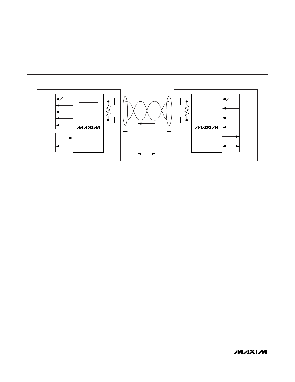
MAX9257/MAX9258
50 ______________________________________________________________________________________
Fully Programmable Serializer/Deserializer
with UART/I2C Control Channel
MAX9258
ECU
μC
CMOS
IMAGE
SENSOR
SERIAL
I/O
MAX9257
SERIAL
I/O
DATA
10
CONTROL UNIT
100Ω 100Ω
REMOTE CAMERA ASSEMBLY
PCLK
HSYNC
VSYNC
LOCK
TX
RX
CONTROL
CHANNEL
DATA
10
PCLK
HSYNC
VSYNC
SERIALIZED
DIGITAL VIDEO
UP TO 20m
CABLE LENGTH
SCL
SDA
Typical Operating Circuit
Page 51

MAX9257/MAX9258
______________________________________________________________________________________ 51
Fully Programmable Serializer/Deserializer
with UART/I2C Control Channel
Package Information
(The package drawing(s) in this data sheet may not reflect the most current specifications. For the latest package outline information,
go to www.maxim-ic.com/packages
.)
QFN THIN.EPS
Page 52

MAX9257/MAX9258
52 ______________________________________________________________________________________
Fully Programmable Serializer/Deserializer
with UART/I2C Control Channel
Package Information (continued)
(The package drawing(s) in this data sheet may not reflect the most current specifications. For the latest package outline information,
go to www.maxim-ic.com/packages
.)
Page 53

MAX9257/MAX9258
______________________________________________________________________________________ 53
Fully Programmable Serializer/Deserializer
with UART/I2C Control Channel
Package Information (continued)
(The package drawing(s) in this data sheet may not reflect the most current specifications. For the latest package outline information,
go to www.maxim-ic.com/packages
.)
32L/48L,LQFP.EPS
PACKAGE OUTLINE, 32/48L LQFP, 7x7x1.4mm
1
21-0054
F
2
Page 54

MAX9257/MAX9258
Maxim cannot assume responsibility for use of any circuitry other than circuitry entirely embodied in a Maxim product. No circuit patent licenses are
implied. Maxim reserves the right to change the circuitry and specifications without notice at any time.
54
____________________Maxim Integrated Products, 120 San Gabriel Drive, Sunnyvale, CA 94086 408-737-7600
© 2008 Maxim Integrated Products is a registered trademark of Maxim Integrated Products, Inc.
Fully Programmable Serializer/Deserializer
with UART/I2C Control Channel
Package Information (continued)
(The package drawing(s) in this data sheet may not reflect the most current specifications. For the latest package outline information,
go to www.maxim-ic.com/packages
.)
PACKAGE OUTLINE, 32/48L LQFP, 7x7x1.4mm
2
21-0054
F
2
 Loading...