

Page 1
19-0115; Rev 3; 3/95
Ultra Low-Power,
Single/Dual-Supply Comparators
_______________General Description
The MAX921–MAX924 single, dual, and quad micropower, low-voltage comparators feature the lowest
power consumption available. These comparators draw
less than 4µA supply current over temperature
(MAX921/MAX922), and include an internal 1.182V
±1% voltage reference, programmable hysteresis, and
TTL/CMOS outputs that sink and source current.
Ideal for 3V or 5V single-supply applications, the
MAX921–MAX924 operate from a single +2.5V to +11V
supply (or a ±1.25V to ±5V dual supply), and each
comparator’s input voltage range swings from the
negative supply rail to within 1.3V of the positive
supply.
The MAX921–MAX924’s unique output stage continuously sources as much as 40mA. And by eliminating
power-supply glitches that commonly occur when comparators change logic states, the MAX921–MAX924
minimize parasitic feedback, which makes them easier to
use.
The single MAX921 and dual MAX923 provide a unique
and simple method for adding hysteresis without
feedback and complicated equations, simply by using
the HYST pin and two resistors.
PART
INTERNAL 1%
PRECISION
REFERENCE
COMPARATORS
PER
PACKAGE
INTERNAL
HYSTERESIS
MAX921 Yes 1 Yes
MAX922 No 2 No
MAX923 Yes 2 Yes
MAX924 Yes 4 No
PACKAGE
8-Pin
DIP/SO/µMAX
8-Pin
DIP/SO/µMAX
8-Pin
DIP/SO/µMAX
16-Pin
DIP/SO/µMAX
________________________Applications
Battery-Powered Systems
Threshold Detectors
Window Comparators
Oscillator Circuits
____________________________Features
♦ µMAX Package—Smallest 8-Pin SO
(MAX921/MAX922/MAX923)
♦ Ultra-Low 4µA Max Quiescent Current
Over Extended Temp. Range (MAX921)
♦ Power Supplies:
Single +2.5V to +11V
Dual ±1.25V to ±5.5V
♦ Input Voltage Range Includes Negative Supply
♦ Internal 1.182V ±1% Bandgap Reference
♦ Adjustable Hysteresis
♦ TTL/CMOS-Compatible Outputs
♦ 12µs Propagation Delay (10mV Overdrive)
♦ No Switching Crowbar Current
♦ 40mA Continuous Source Current
______________Ordering Information
PART TEMP. RANGE PIN-PACKAGE
MAX921CPA
MAX921CSA 0°C to +70°C 8 SO
MAX921CUA 0°C to +70°C 8 µMAX
MAX921C/D 0°C to +70°C Dice*
MAX921EPA -40°C to +85°C 8 Plastic DIP
MAX921ESA -40°C to +85°C 8 SO
MAX921MJA -55°C to +125°C 8 CERDIP**
Ordering Information continued at end of data sheet.
* Dice are tested at T
** Contact factory for availability and processing to MIL-STD-883.
0°C to +70°C 8 Plastic DIP
= +25°C, DC parameters only.
A
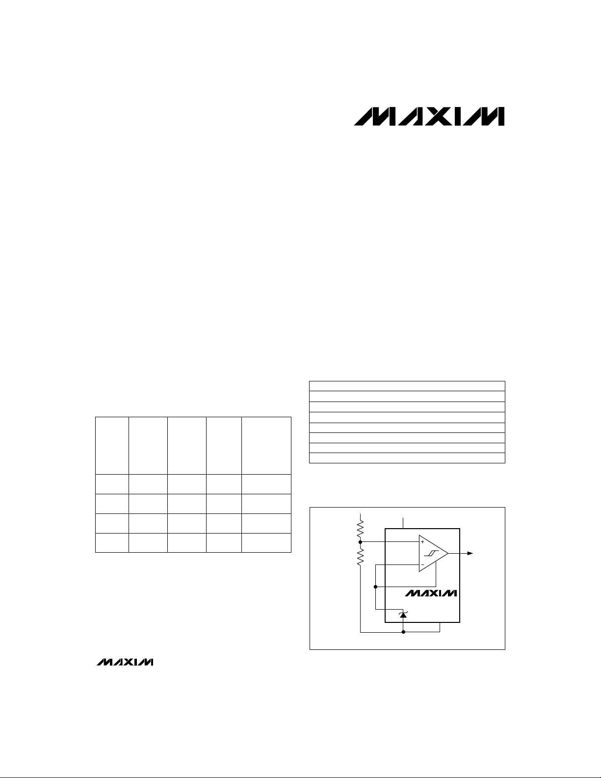
__________Typical Operating Circuit
V
IN
7
V+
3
IN+
8
OUT
IN-
4
HYST
5
REF
6
THRESHOLD DETECTOR
MAX921
V-
GND
21
MAX921–MAX924
________________________________________________________________
Maxim Integrated Products
Call toll free 1-800-998-8800 for free samples or literature.
1
Page 2
Ultra Low-Power,
Single/Dual-Supply Comparators
ABSOLUTE MAXIMUM RATINGS
V+ to V-, V+ to GND, GND to V-................................-0.3V, +12V
Inputs
Current, IN_+, IN_-, HYST...............................................20mA
Voltage, IN_+, IN_-, HYST................(V+ + 0.3V) to (V- – 0.3V)
Outputs
Current, REF....................................................................20mA
Current, OUT_.................................................................50mA
Voltage, REF ....................................(V+ + 0.3V) to (V- – 0.3V)
Voltage, OUT_ (MAX921/924).....(V+ + 0.3V) to (GND – 0.3V)
Voltage OUT_ (MAX922/923)...........(V+ + 0.3V) to (V- – 0.3V)
OUT_ Short-Circuit Duration (V+ ≤ 5.5V) ...............Continuous
Stresses beyond those listed under “Absolute Maximum Ratings‘” may cause permanent damage to the device. These are stress ratings only, and functional
operation of the device at these or any other conditions beyond those indicated in the operational sections of the specifications is not implied. Exposure to
MAX921–MAX924
absolute maximum rating conditions for extended periods may affect device reliability.
ELECTRICAL CHARACTERISTICS: 5V OPERATION
(V+ = 5V, V- = GND = 0V, TA= T
PARAMETER
POWER REQUIREMENTS
Supply Voltage Range
Supply Current IN+ = IN- + 100mV
COMPARATOR
Input Offset Voltage
Input Leakage Current (HYST)
Input Common-Mode Voltage Range
Common-Mode Rejection Ratio
Power-Supply Rejection Ratio
Voltage Noise
Hysteresis Input Voltage Range REF- 0.05V REF V
to T
MIN
, unless otherwise noted.)
MAX
(Note 1)
VCM= 2.5V
IN+ = IN- = 2.5V
MAX921, MAX923
V- to (V+ – 1.3V)
V+ = 2.5V to 11V
100Hz to 100kHz
MAX921, MAX923
TA= +25°C, 100pF load
CONDITIONS
Continuous Power Dissipation (TA= +70°C)
8-Pin Plastic DIP (derate 9.09mW/°C above +70°C) ...727mW
8-Pin SO (derate 5.88mW/°C above +70°C)................471mW
8-Pin µMAX (derate 4.1mW/°C above +70°C).............330mW
8-Pin CERDIP (derate 8.00mW/°C above +70°C)........640mW
16-Pin Plastic DIP (derate 10.53mW/°C above +70°C)..842mW
16-Pin SO (derate 8.70mW/°C above +70°C)................696mW
16-Pin CERDIP (derate 10.00mW/°C above +70°C)......800mW
Operating Temperature Ranges:
MAX92_C_ _ .......................................................0°C to +70°C
MAX92_E_ _.....................................................-40°C to +85°C
MAX92_MJ_ ..................................................-55°C to +125°C
Storage Temperature Range.............................-65°C to +150°C
Lead Temperature (soldering, 10sec).............................+300°C
MIN TYP MAX UNITS
2.5 11 V
MAX921,
HYST = REF
MAX922
MAX923,
HYST = REF
MAX924
TA= +25°C
C/E temp. ranges
M temp. range
TA= +25°C
C/E temp. ranges
M temp. range
TA= +25°C
C/E temp. ranges
M temp. range
TA= +25°C
C/E temp. ranges
M temp. range
C/E temp. ranges
M temp. range
Overdrive = 10mV
Overdrive = 100mV
2.5 3.2
2.5 3.2
3.1 4.5
5.5 6.5
±0.01 ±5
±0.02 nA
0.1 1.0 mV/V
0.1 1.0 mV/V
20 µV
12
4
4
5
4
5
6
7.5
8.5
11
±10 mV
±40
µA
nAInput Leakage Current (IN-, IN+)
VV- V+ – 1.3
RMS
µsResponse Time
2 _______________________________________________________________________________________
Page 3
Ultra Low-Power,
Single/Dual-Supply Comparators
ELECTRICAL CHARACTERISTICS: 5V OPERATION (continued)
(V+ = 5V, V- = GND = 0V, TA= T
PARAMETER
Output Low Voltage
REFERENCE (MAX921/MAX923/MAX924 ONLY)
X
Sink Current
Voltage Noise
Note 1: MAX924 comparators work below 2.5V, see
to T
MIN
, unless otherwise noted.)
MAX
CONDITIONS
MAX92_
MAX922/
MAX923
MAX921/
MAX924
100Hz to 100kHz 100 µV
C/E temp. ranges: I
M temp. range: I
C/E temp. ranges: I
M temp. range: I
C/E temp. ranges: I
M temp. range: I
Low-Voltage Operation
= 17mA;
OUT
= 10mA
OUT
= 1.8mA;
OUT
= 1.2mA
OUT
= 1.8mA;
OUT
= 1.2mA
OUT
C temp. range
E temp. range
M temp. range
TA= +25°C
M temp. range 4
TA= +25°C
C/E temp. ranges 4
M temp. range
section for more details.
ELECTRICAL CHARACTERISTICS: 3V OPERATION
(V+ = 3V, V- = GND = 0V, TA= T
PARAMETER
POWER REQUIREMENTS
Supply Current
COMPARATOR
Input Offset Voltage
Input Leakage Current (HYST)
MIN
to T
, unless otherwise noted.)
MAX
CONDITIONS
HYST = REF,
IN+ = (IN- + 100mV)
VCM= 1.5V
IN+ = IN- = 1.5V
MAX921, MAX923
MAX921
MAX922
MAX923
MAX924
TA= +25°C
C/E temp. ranges
M temp. range
TA= +25°C
C/E temp. ranges
M temp. range
TA= +25°C
C/E temp. ranges
M temp. range
TA= +25°C
C/E temp. ranges
M temp. range
C/E temp. ranges
M temp. range
MIN TYP MAX UNITS
V+ – 0.4
V- + 0.4
GND + 0.4
1.170 1.182 1.194
1.158 1.206Reference Voltage
1.147 1.217
15 25
815
2
MIN TYP MAX UNITS
2.4 3.0
3.8
4.8
2.4 3.0
3.8
4.8
3.4 4.3
5.8
7.2
5.2 6.2
8.0
10.5
±10 mV
±0.01 ±5
±40
±0.02 nA
MAX921–MAX924
VOutput High Voltage
V
V
µAC/E temp. ranges 6Source Current
µA
RMS
µA
nAInput Leakage Current (IN-, IN+)
_______________________________________________________________________________________ 3
Page 4
Ultra Low-Power,
Single/Dual-Supply Comparators
ELECTRICAL CHARACTERISTICS: 3V OPERATION (continued)
(V+ = 3V, V- = GND = 0V, TA= T
MIN
to T
, unless otherwise noted.)
MAX
PARAMETER
CONDITIONS
MIN TYP MAX UNITS
Input Common-Mode Voltage Range VV- V+ – 1.3
Common-Mode Rejection Ratio 0.2 1 mV/V
Power-Supply Rejection Ratio
Voltage Noise
Hysteresis Input Voltage Range REF- 0.05V REF V
MAX921–MAX924
Output Low Voltage
V- to (V+ – 1.3V)
V+ = 2.5V to 11V
100Hz to 100kHz
MAX921, MAX923
TA= +25°C, 100pF load
MAX92_
MAX922/
MAX923
MAX921/
MAX924
C/E temp. ranges: I
M temp. range: I
C/E temp. ranges: I
M temp. range: I
C/E temp. ranges: I
M temp. range: I
Overdrive = 10mV
Overdrive = 100mV
= 10mA;
OUT
= 6mA
OUT
= 0.8mA;
OUT
= 0.6mA
OUT
= 0.8mA;
OUT
= 0.6mA
OUT
0.1 1 mV/V
20 µV
14
5
V+ – 0.4
V- + 0.4
GND + 0.4
REFERENCE
Source Current
C temp. range
E temp. range
M temp. range
TA= +25°C
C/E temp. ranges 6
1.170 1.182 1.194
1.158 1.206Reference Voltage
1.147 1.217
15 25
M temp. range 4
Sink Current
Voltage Noise
TA= +25°C
C/E temp. ranges 4
M temp. range
100Hz to 100kHz 100 µV
815
2
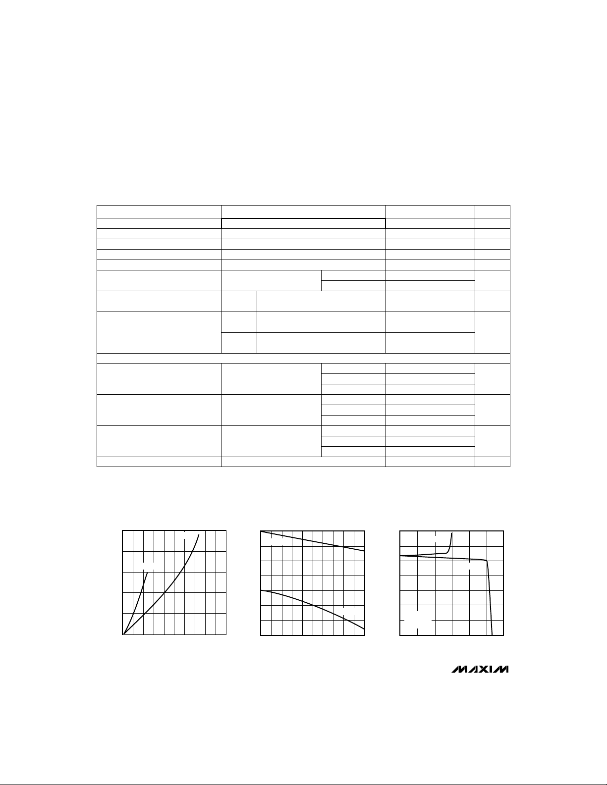
__________________________________________Typical Operating Characteristics
(V+ = 5V, V- = GND, TA = +25°C, unless otherwise noted).
OUTPUT VOLTAGE LOW
vs. LOAD CURRENT
2.5
2.0
V+ = 3V
48 16
020
(V)
OL
V
1.5
1.0
0.5
0.0
V+ = 5V
12
LOAD CURRENT (mA)
MAX921/4-TOC1
(V)
OH
V
5.0
4.5
4.0
3.5
3.0
2.5
2.0
1.5
OUTPUT VOLTAGE HIGH vs.
V+ = 5V
010 30 50
LOAD CURRENT
MAX921/924-TOC2
V+ = 3V
20 40
LOAD CURRENT (mA)
REFERENCE OUTPUT VOLTAGE vs.
OUTPUT LOAD CURRENT
1.190
1.185
1.180
1.175
1.170
1.165
REFERENCE OUTPUT VOLTAGE (V)
1.160
1.155
0 5 15 25
SINK
V+ = 5V
OR
V+ = 3V
10 20
OUTPUT LOAD CURRENT (µA)
SOURCE
RMS
µsResponse Time
VOutput High Voltage
V
V
µA
µA
RMS
MAX921/924-TOC3
30
4 _______________________________________________________________________________________
Page 5
Ultra Low-Power,
Single/Dual-Supply Comparators
__________________________________________Typical Operating Characteristics
(V+ = 5V, V- = GND, TA = +25°C, unless otherwise noted).
REFERENCE VOLTAGE
vs. TEMPERATURE
1.22
1.21
1.20
1.19
1.18
1.17
1.16
REFERENCE VOLTAGE (V)
1.15
1.14
MILITARY TEMP. RANGE
EXTENDED TEMP. RANGE
COMMERCIAL
TEMP. RANGE
-60 -20 60 140
-40 0 8040 120
20 100
TEMPERATURE (°C)
MAX923
SUPPLY CURRENT vs. TEMPERATURE
5.0
4.5
4.0
3.5
3.0
SUPPLY CURRENT (µA)
2.5
2.0
V+ = 5V, V- = 0V
V+ = 3V, V- = 0V
-60 140
-20 20 100
TEMPERATURE (°C)
60
HYSTERESIS CONTROL
80
60
OUTPUT HIGH
40
20
0
IN+ – IN- (V)
-20
-40
OUTPUT LOW
-60
-80
010 30 50
NO CHANGE
20 40
V
-V
(mV)
REF
HYST
_______________________________________________________________________________________
4.5
IN+ = IN- + 100mV
4.0
MAX921/924-TOC4
V+ = 5V, V- = -5V
3.5
3.0
SUPPLY CURRENT (µA)
2.5
2.0
-60 140
SUPPLY CURRENT vs. TEMPERATURE
10
IN+ = (IN- + 100mV)
9
MAX921/924-TOC7
8
7
V+ = 5V, V- = -5V
6
5
SUPPLY CURRENT (µA)
4
3
-60 140
5.0
4.5
4.0
MAX921/924 TOC10
3.5
3.0
2.5
2.0
1.5
OUTPUT VOLTAGE (V)
1.0
0.5
0
-0.3 -0.1 0.3
MAX921
SUPPLY CURRENT vs.
TEMPERATURE
V+ = 3V, V- = 0V
V+ = 5V, V- = 0V
-20 20 100
TEMPERATURE (°C)
60
MAX924
V+ = 5V, V- = 0V
V+ = 3V, V- = 0V
-20 20 100
TEMPERATURE (°C)
60
TRANSFER FUNCTION
100k
V
0
10µF
-0.2 0
IN+ INPUT VOLTAGE (mV)
0.1
SUPPLY CURRENT vs. TEMPERATURE
MAX922
4.5
IN+ = (IN- + 100mV)
4.0
MAX921/924-TOC5
3.5
V+ = 10V, V- = 0V
3.0
2.5
SUPPLY CURRENT (µA)
2.0
1.5
-60 140
V+ = 3V, V- = 0V
-20 20 100
TEMPERATURE (°C)
V+ = 5V, V- = 0V
60
MAX924
SUPPLY CURRENT vs.
LOW SUPPLY VOLTAGES
10
MAX921/924-TOC8
1
0.1
SUPPLY CURRENT (µA)
0.01
1.0 2.0 2.5
1.5
SINGLE-SUPPLY VOLTAGE (V)
RESPONSE TIME vs.
LOAD CAPACITANCE
18
V- = 0V
16
MAX921/924-TOC11
14
12
10
8
RESPONSE TIME (µs)
6
4
0.2
2
0 20 60 100
V
OHL
V
OLH
40 80
LOAD CAPACITANCE (nF)
MAX921-MAX924
MAX921/924-TOC6
MAX921/924-TOC9
MAX921/924 TOC12
5
Page 6

Ultra Low-Power,
Single/Dual-Supply Comparators
__________________________________________Typical Operating Characteristics
(V+ = 5V, V- = GND, TA = +25°C, unless otherwise noted).
RESPONSE TIME FOR VARIOUS
INPUT OVERDRIVES
5
4
100mV
3
2
50mV
1
OUTPUT VOLTAGE (V)
0
0
100
MAX921–MAX924
-2 2 10 18
INPUT VOLTAGE (mV)
20mV
10mV
614
RESPONSE TIME (µs)
MAX924 RESPONSE TIME
AT LOW SUPPLY VOLTAGES
100
SOURCE CURRENT INTO 0.75V LOAD
10
CURRENT (mA)
1
SINK CURRENT AT V
0.1
1.0 2.0 2.5
1.5
SINGLE-SUPPLY VOLTAGE (V)
OUT
= 0.4V
5
MAX921/924-TOC13
4
3
100mV
2
1
OUTPUT VOLTAGE (V)
50mV
0
100
0
-2 2 10 18
INPUT VOLTAGE (mV)
SHORT-CIRCUIT SOURCE CURRENT
200
180
OUT CONNECTED TO V-
160
MAX921/924-TOC16
140
120
100
80
60
SOURCE CURRENT (mA)
40
20
0
0 1.0 3.0 5.0
RESPONSE TIME FOR VARIOUS
INPUT OVERDRIVES
10mV
20mV
614
RESPONSE TIME (µs)
vs. SUPPLY VOLTAGE
2.0 4.0
TOTAL SUPPLY VOLTAGE (V)
MAX924 RESPONSE TIME
AT LOW SUPPLY VOLTAGES
10
MAX921/924-TOC14
1
0.1
RESPONSE TIME (ms)
±100mV
OVERDRIVE
0.01
1.0 2.0 2.5
±20mV OVERDRIVE
1.5
SINGLE-SUPPLY VOLTAGE (V)
MAX921/924-TOC15
SHORT-CIRCUIT SINK CURRENT
vs. SUPPLY VOLTAGE
OUT CONNECTED TO V+
MAX121/124-TOC17
GND CONNECTED TO V-
20
10
SINK CURRENT (mA)
0
010
TOTAL SUPPLY VOLTAGE (V)
5
MAX121/124-TOC18
____________________________________________________________Pin Descriptions
PIN
MAX921 MAX922 MAX923
1 – – GND Ground. Connect to V- for single-supply operation. Output swings from V+ to GND.
– 1 OUTA Comparator A output. Sinks and sources current. Swings from V+ to V-.
1
2 2 2 V- Negative supply. Connect to ground for single-supply operation (MAX921).
3 – – IN+ Noninverting comparator input
– 3 3 INA+ Noninverting input of comparator A
4 – – IN- Inverting comparator input
– 4 – INA- Inverting input of comparator A
6 _______________________________________________________________________________________
NAME FUNCTION
Page 7

Ultra Low-Power,
Single/Dual-Supply Comparators
_______________________________________________Pin Descriptions (continued)
PIN
MAX921 MAX922 MAX923
– 5 4 INB- Inverting input of comparator B
5 5 HYST
6 – 6 REF Reference output. 1.182V with respect to V-.
– 6 –
7 7 7 V+ Positive supply
8 – – OUT Comparator output. Sinks and sources current. Swings from V+ to GND.
– 8 8 OUTB Comparator B output. Sinks and sources current. Swings from V+ to V-.
PIN
MAX924
10 INC- Inverting input of comparator C
11 INC+ Noninverting input of comparator C
12 IND- Inverting input of comparator D
13 IND+ Noninverting input of comparator D
14 GND Ground. Connect to V- for single-supply operation.
15 OUTD Comparator D output. Sinks and sources current. Swings from V+ to GND.
16 OUTC Comparator C output. Sinks and sources current. Swings from V+ to GND.
–
NAME FUNCTION
1 OUTB Comparator B output. Sinks and sources current. Swings from V+ to GND.
2 OUTA Comparator A output. Sinks and sources current. Swings from V+ to GND.
3 V+ Positive supply
4 INA- Inverting input of comparator A
5 INA+ Noninverting input of comparator A
6 INB- Inverting input of comparator B
7 INB+ Noninverting input of comparator B
8 REF Reference output. 1.182V with respect to V-.
9 V- Negative supply. Connect to ground for single-supply operation.
NAME FUNCTION
Hysteresis input. Connect to REF if not used. Input voltage range is from
V
to V
REF
- 50mV.
INB+
REF
Noninverting input of comparator B
MAX921–MAX924
_______________________________________________________________________________________ 7
Page 8

Ultra Low-Power,
Single/Dual-Supply Comparators
_______________Detailed Description
The MAX921–MAX924 comprise various combinations
of a micropower 1.182V reference and a micropower
comparator. The
MAX921 configuration, and Figures 1a-1c show the
MAX922–MAX924 configurations.
Each comparator continuously sources up to 40mA,
and the unique output stage eliminates crowbar
glitches during output transitions. This makes them
immune to parasitic feedback (which can cause
instability) and provides excellent performance, even
when circuit-board layout is not optimal.
Internal hysteresis in the MAX921 and MAX923 provides
the easiest method for implementing hysteresis. It also
produces faster hysteresis action and consumes much
less current than circuits using external positive feedback.
MAX921–MAX924
Power-Supply and Input Signal Ranges
This family of devices operates from a single +2.5V to
+11V power supply. The MAX921 and MAX924 have a
Figure 1a. MAX922 Functional Diagram
Typical Operating Circuit
OUTA
1
V-
2
INA+
3
4
INA-
MAX922
OUTB
INB+
INB-
8
V+
7
6
5
shows the
separate ground for the output driver, allowing
operation with dual supplies ranging from ±1.25V to
±5.5V. Connect V- to GND when operating the
MAX921 and the MAX924 from a single supply. The
maximum supply voltage in this case is still 11V.
For proper comparator operation, the input signal can
swing from the negative supply (V-) to within one volt of
the positive supply (V+ – 1V). The guaranteed
common-mode input voltage range extends from V- to
(V+ - 1.3V). The inputs can be taken above and below
the supply rails by up to 300mV without damage.
Operating the MAX921 and MAX924 at ±5V provides
TTL/CMOS compatibility when monitoring bipolar input
signals. TTL compatibility for the MAX922 and MAX923
is achieved by operation from a single +5V supply.
Low-Voltage Operation: V+ = 1V (MAX924 Only)
The guaranteed minimum operating voltage is 2.5V (or
±1.25V). As the total supply voltage is reduced below
2.5V, the performance degrades and the supply
current falls. The reference will not function below
1
OUTB
OUTA
2
V+
3
INA-
4
5
INA+
MAX924
OUTC
OUTD
GND
IND+
IND-
16
15
14
13
12
INB-
OUTA
1
V-
2
INA+
3
4
INB-
MAX923
V-
Figure 1b. MAX923 Functional Diagram
8 _______________________________________________________________________________________
OUTB
REF
HYST
8
V+
7
6
5
Figure 1c. MAX924 Functional Diagram
6
7
INB+
8
REF
INC+
INC-
11
10
9
V-
Page 9

Ultra Low-Power,
Single/Dual-Supply Comparators
IN+
IN-
VREF - VHYST
OUT
Figure 2. Threshold Hysteresis Band
V
HB
THRESHOLDS
HYSTERESIS
BAND
about 2.2V, although the comparators will continue to
operate with a total supply voltage as low as 1V. While
the MAX924 has comparators that may be used at
supply voltages below 2V, the MAX921, MAX922, and
MAX923 may not be used with supply voltages significantly below 2.5V.
At low supply voltages, the comparators’ output drive is
reduced and the propagation delay increases (see
Typical Operating Characteristics
). The useful input
voltage range extends from the negative supply to a
little under 1V below the positive supply, which is
slightly closer to the positive rail than the device
operating from higher supply voltages. Test your
prototype over the full temperature and supply-voltage
range if operation below 2.5V is anticipated.
Comparator Output
With 100mV of overdrive, propagation delay is typically
3µs. The
Typical Operating Characteristics
show the
propagation delay for various overdrive levels.
The MAX921 and MAX924 output swings from V+ to
GND, so TTL compatibility is assured by using a +5V
±10% supply. The negative supply does not affect the
output swing, and can range from 0V to -5V ±10%.
The MAX922 and MAX923 have no GND pin, and their
outputs swing from V+ to V-. Connect V- to ground and
V+ to a +5V supply to achieve TTL compatibility.
The MAX921–MAX924’s unique design achieves an
output source current of more than 40mA and a sink
current of over 5mA, while keeping quiescent currents in
the microampere range. The output can source 100mA
(at V+ = 5V) for short pulses, as long as the package's
maximum power dissipation is not exceeded. The
output stage does not generate crowbar switching
currents during transitions, which minimizes feedback
through the supplies and helps ensure stability without
bypassing.
Voltage Reference
The internal bandgap voltage reference has an output
of 1.182V above V-. Note that the REF voltage is
referenced to V-, not to GND. Its accuracy is ±1% in
the range 0°C to +70°C. The REF output is typically
capable of sourcing 15µA and sinking 8µA. Do not
bypass the REF output.
Noise Considerations
Although the comparators have a very high gain, useful
gain is limited by noise. This is shown in the Transfer
Function graph (see
Typical Operating Characteristics
As the input voltage approaches the comparator's
offset, the output begins to bounce back and forth; this
peaks when VIN= VOS. (The lowpass filter shown on
the graph averages out the bouncing, making the
transfer function easy to observe.) Consequently, the
comparator has an effective wideband peak-to-peak
noise of around 0.3mV. The voltage reference has
peak-to peak noise approaching 1mV. Thus, when a
2.5V TO 11V
I
REF
R1
R2
Figure 3. Programming the HYST Pin
7
6
V+
REF
MAX921
MAX923
5
HYST
V-
2
MAX921–MAX924
).
_______________________________________________________________________________________ 9
Page 10
Ultra Low-Power,
Single/Dual-Supply Comparators
comparator is used with the reference, the combined
peak-to-peak noise is about 1mV. This, of course, is
much higher than the RMS noise of the individual
components. Care should be taken in the layout to
avoid capacitive coupling from any output to the
reference pin. Crosstalk can significantly increase the
actual noise of the reference.
__________Applications Information
Hysteresis increases the comparators’ noise margin by
increasing the upper threshold and decreasing the
lower threshold (see Figure 2).
Hysteresis (MAX921/MAX923)
To add hysteresis to the MAX921 or MAX923, connect
resistor R1 between REF and HYST, and connect
MAX921–MAX924
resistor R2 between HYST and V- (Figure 3). If no
hysteresis is required, connect HYST to REF. When
hysteresis is added, the upper threshold increases by
the same amount that the lower threshold decreases.
The hysteresis band (the difference between the upper
and lower thresholds, VHB) is approximately equal to
twice the voltage between REF and HYST. The HYST
input can be adjusted to a maximum voltage of REF
and to a minimum voltage of (REF – 50mV). The
maximum difference between REF and HYST (50mV)
will therefore produce a 100mV max hysteresis band.
Use the following equations to determine R1 and R2:
V
R1 =
R2 =
Where I
should not exceed the REF source capability, and
HB
×
2 I
()
REF
1.182 –
REF
V
HB
2
I
REF
(the current sourced by the reference)
should be significantly larger than the HYST input
current. I
usually appropriate. If 2.4MΩ is chosen for R2 (I
values between 0.1µA and 4µA are
REF
0.5µA), the equation for R1 and VHBcan be
approximated as:
R1 (k ) = V (mV)
Ω
HB
When hysteresis is obtained in this manner for the
MAX923, the same hysteresis applies to both comparators.
Hysteresis (MAX922/MAX924)
Hysteresis can be set with two resistors using positive
feedback, as shown in Figure 4. This circuit generally
draws more current than the circuits using the HYST
pin on the MAX921 and MAX923, and the high
Hysteresis
REF
feedback impedance slows hysteresis. The design
procedure is as follows:
1. Choose R3. The leakage current of IN+ is under
1nA (up to +85°C), so the current through R3 can be
around 100nA and still maintain good accuracy.
The current through R3 at the trip point is V
or 100nA for R3 = 11.8MΩ. 10MΩ is a good
practical value.
2. Choose the hysteresis voltage (VHB), the voltage
between the upper and lower thresholds. In this
example, choose VHB= 50mV.
3. Calculate R1.
V
R1 = R3
=×
10M
=Ω
100k
HB
×
+
V
0.05
5
4. Choose the threshold voltage for VINrising (V
In this example, choose V
THR
= 3V.
5. Calculate R2.
R2 =
(V
=
(1.182 100k)1100k110M
65.44k
=
REF R1)
V
THR
×
3
×
Ω
1
1R11
−−
1
R3
−−
A 1% preferred value is 64.9kΩ.
V+
R3
R1
V
=
IN
R2
V
Figure 4. External Hysteresis
V+
MAX924
GND
REF
OUT
V-
REF
/R3,
THR
).
10 ______________________________________________________________________________________
Page 11

Ultra Low-Power,
Single/Dual-Supply Comparators
MOMENTARY
GND
SWITCH
IN+
3
OUT
8
C
VBATT -0.15V
10mA
R
4.5V TO 6.0V
7
V+
6
REF
47k
5
HYST
1.1M
IN-
4
100k
Figure 5. Auto-off power switch operates on 2.5µA quiescent
current.
MAX921
V-
21
6. Verify the threshold voltages with these formulas:
V rising:
IN
1
1
R2
1
R3
=××++
V V R1
THR REF
V falling:
IN
V V
=−
THF THR
R1
R1 V
×+
()
R3
Board Layout and Bypassing
Power-supply bypass capacitors are not needed if the
supply impedance is low, but 100nF bypass capacitors
should be used when the supply impedance is high or
when the supply leads are long. Minimize signal lead
lengths to reduce stray capacitance between the input
and output that might cause instability. Do not bypass
the reference output.
_______________Typical Applications
Figure 5 shows the schematic for a 40mA power supply
that has a timed auto power-off function. The
comparator output is the switched power-supply
output. With a 10mA load, it typically provides a
voltage of (V
quiescent current. This circuit takes advantage of the
BATT
four key features of the MAX921: 2.5µA supply current,
an internal reference, hysteresis, and high current
output. Using the component values shown, the threeresistor voltage divider programs the maximum ±50mV
of hysteresis and sets the IN- voltage at 100mV. This
gives an IN+ trip threshold of approximately 50mV for
IN+ falling.
The RC time constant determines the maximum poweron time of the OUT pin before power-down occurs.
This period can be approximated by:
For example: 2MΩ x 10µF x 4.6 = 92sec. The actual
time will vary with both the leakage current of the
capacitor and the voltage applied to the circuit.
The MAX923 is ideal for making window detectors
(undervoltage/overvoltage detectors). The schematic
is shown in Figure 6, with component values selected
for an 4.5V undervoltage threshold, and a 5.5V
overvoltage threshold. Choose different thresholds by
changing the values of R1, R2, and R3. To prevent
chatter at the output when the supply voltage is close
to a threshold, hysteresis has been added using R4
and R5. OUTA provides an active-low undervoltage
indication, and OUTB gives an active-low overvoltage
indication. ANDing the two outputs provides an activehigh, power-good signal.
The design procedure is as follows:
1. Choose the required hysteresis level and calculate
values for R4 and R5 according to the formulas in
the
Hysteresis (MAX921/MAX923)
example, ±5mV of hysteresis has been added
comparator input
hysteresis apparent at VINwill be larger because of
the input resistor divider.
Auto-Off Power Source
– 0.12V), but draws only 3.5µA
R x C x 4.6sec
Window Detector
section. In this
at the
(VH= VHB/2). This means that the
MAX921–MAX924
______________________________________________________________________________________ 11
Page 12

Ultra Low-Power,
Single/Dual-Supply Comparators
2. Select R1. The leakage current into INB- is normally
under 1nA, so the current through R1 should
exceed 100nA for the thresholds to be accurate. R1
values up to about 10MΩ can be used, but values in
the 100kΩ to 1MΩ range are usually easier to deal
with. In this example, choose R1 = 294kΩ.
3. Calculate R2 + R3. The overvoltage threshold
should be 5.5V when VINis rising. The design
equation is as follows:
V
R2 R3 R1
+=×
294k
=×
1.068M
MAX921–MAX924
4. Calculate R2. The undervoltage threshold should
=Ω
OTH
+
V V
REF H
(1.182 0.005)
−
1
5.5
+
1
−
be 4.5V when VINis falling. The design equation is
as follows:
(V V )
−
R2 (R1 + R2 + R3)
=×
(294k + 1.068M)
=×
62.2k
=
Ω
Choose R2 61.9k (1% standard value).
=
REF H
V
(1.182 0.005)
Ω
R1
UTH
−
−
294k
4.5
−
5. Calculate R3.
R3 (R2 + R3) R2
=−
.068M 6 k
=−
119 .
1.006M
=
Ω
Choose R3 = 1MΩ (1% standard value)
6. Verify the resistor values. The equations are as
follows, evaluated for the above example.
Overvoltage threshold:
++
=+×
V (V V )
OTH REF H
=
5.474V.
Undervoltage threshold:
=−×
V (V V )
UTH REF H
=
4.484V,
where the hysteresis voltage V V
(R1 R2 R3)
R1
++
(R1 R2 R3)
(R1 + R2)
=×
H REF
R5
R4
.
V
V
OTH
IN
V
UTH
R3
10k
R2
R5
R4
2.4M
R1
Figure 6. Window Detector
The high output source capability of the MAX921 series
is useful for driving LEDs. An example of this is the
simple four-stage level detector shown in Figure 7.
The full-scale threshold (all LEDs on) is given by VIN=
(R1 + R2)/R1 volts. The other thresholds are at 3/4 full
scale, 1/2 full scale, and 1/4 full scale. The output
resistors limit the current into the LEDs.
Figure 8 shows a circuit to shift from bipolar ±5V inputs
to TTL signals. The 10kΩ resistors protect the
comparator inputs, and do not materially affect the
operation of the circuit.
= 5.5V
= 4.5V
INA+
HYST
REF
INB-
+5V
V+
OUTA
OUTB
V-
MAX923
Bar-Graph Level Gauge
UNDERVOLTAGE
POWER GOOD
OVERVOLTAGE
Level Shifter
12 ______________________________________________________________________________________
Page 13

Ultra Low-Power,
Single/Dual-Supply Comparators
MAX921–MAX924
182k
250k
250k
250k
250k
R1
1.182V
750mV
500mV
250mV
R2
+5V
3
V+
8
REF
5
INA+
4
1V
INA-
7
INB+
INB-
6
INC+
11
10
INC-
13
IND+
12
IND-
MAX924
GND
14
OUTA
OUTB
OUTC
OUTD
V
IN
10k
V
INA
9
V-
2
330Ω
1
330Ω
16
330Ω
15
330Ω
10k
V
INB
10k
V
INC
10k
V
IND
INA+
INA-
INB+
INB-
INC+
INC-
IND+
IND-
+5V
GND
V+
MAX924
OUTA
0 FOR V
< 0V
INA
> 0V
1 FOR V
INB
OUTB
OUTC
OUTD
REFV-N.C.
-5V
Figure 7. Bar-Graph Level Gauge Figure 8. Level Shifter: ±5V Input to CMOS Output
______________________________________________________________________________________ 13
Page 14
Ultra Low-Power,
Single/Dual-Supply Comparators
_________________Pin Configurations _Ordering Information (continued)
TOP VIEW
GND
IN+
IN-
1
2
V-
MAX921
3
4
8
7
6
5
DIP/SO/µMAX
1
OUTA
2
V-
MAX921–MAX924
INA+
INA-
3
4
MAX922
8
7
6
5
DIP/SO/µMAX
OUTA
INA+
INB-
1
2
V-
MAX923
3
4
8
7
6
5
OUT
V+
REF
HYST
OUTB
V+
INB+
INB-
OUTB
V+
REF
HYST
PART TEMP. RANGE PIN-PACKAGE
MAX922CPA
0°C to +70°C 8 Plastic DIP
MAX922CSA 0°C to +70°C 8 SO
MAX922CUA 0°C to +70°C 8 µMAX
MAX922C/D 0°C to +70°C Dice*
MAX922EPA -40°C to +85°C 8 Plastic DIP
MAX922ESA -40°C to +85°C 8 SO
MAX922MJA -55°C to +125°C 8 CERDIP**
MAX923CPA
0°C to +70°C 8 Plastic DIP
MAX923CSA 0°C to +70°C 8 SO
MAX923CUA 0°C to +70°C 8 µMAX
MAX923C/D 0°C to +70°C Dice*
MAX923EPA -40°C to +85°C 8 Plastic DIP
MAX923ESA -40°C to +85°C 8 SO
MAX923MJA -55°C to +125°C 8 CERDIP**
MAX924CPE
0°C to +70°C 16 Plastic DIP
MAX924CSE 0°C to +70°C 16 Narrow SO
MAX924C/D 0°C to +70°C Dice*
MAX924EPE -40°C to +85°C 16 Plastic DIP
MAX924ESE -40°C to +85°C 16 Narrow SO
MAX924MJE -55°C to +125°C 16 CERDIP**
* Dice are tested at TA= +25°C, DC parameters only.
** Contact factory for availability and processing to MIL-STD-883.
DIP/SO/µMAX
OUTB
OUTA
INAINA+
INB-
INB+
REF
1
2
V+
3
MAX924
4
5
6
7
8
OUTC
16
OUTD
15
GND
14
IND+
13
IND-
12
INC+
11
INC-
10
V-
9
DIP/Narrow SO
14 ______________________________________________________________________________________
Page 15

Ultra Low-Power,
Single/Dual-Supply Comparators
__________________________________________________________Chip Topographies
MAX921/MAX922/MAX923 MAX924
OUTB OUTC
V-
0.069"
(1.75mm)
OUTD
GND
0.108"
(2.74mm)
IND+
IND-
INC+
INC-REFINB+
1
2
3
4
5
0.059"
(1.50mm)
DIE PAD MAX921 MAX922 MAX923
1 GND OUTA OUTA
2V-V-V3V-V-V4 IN+ INA+ INA+
5 IN- INA- INB6 HYST INB- HYST
7 REF INB+ REF
8 V+V+V+
9 V+V+V+
10 OUT OUTB OUTB
TRANSISTOR COUNT: 164
SUBSTRATE CONNECTED TO V+
10
9
8
0.075"
(1.91mm)
7
6
OUTA
V+
INA-
INA+
INB-
TRANSISTOR COUNT: 267
SUBSTRATE CONNECTED TO V+
MAX921–MAX924
______________________________________________________________________________________ 15
Page 16

Ultra Low-Power,
Single/Dual-Supply Comparators
_______________________________________________________Package Information
INCHES MILLIMETERS
DIM
A
A1
B
C
D
E
e
H
L
α
0.101mm
0.004 in
C
L
A
e
A1B
α
MIN
0.036
0.004
0.010
0.005
0.116
0.116
0.188
0.016
0°
MAX
MIN
0.044
0.91
0.008
0.10
0.014
0.25
0.007
0.13
0.120
2.95
0.120
2.95
0.198
0.026
4.78
0.41
6°
0°
MAX921–MAX924
E H
8-PIN µMAX
MICROMAX SMALL-OUTLINE
PACKAGE
D
INCHES MILLIMETERS
DIM
D
A
0.101mm
e
A1
B
0.004in.
C
0°-8°
L
A
A1
B
C
E
e
H
L
MIN
0.053
0.004
0.014
0.007
0.150
0.228
0.016
MAX
MIN
0.069
1.35
0.010
0.10
0.019
0.35
0.010
0.19
0.157
3.80
0.244
0.050
5.80
0.40
0.650.0256
1.270.050
MAX
1.11
0.20
0.36
0.18
3.05
3.05
5.03
0.66
6°
21-0036D
MAX
1.75
0.25
0.49
0.25
4.00
6.20
1.27
Narrow SO
HE
SMALL-OUTLINE
PACKAGE
(0.150 in.)
Maxim cannot assume responsibility for use of any circuitry other than circuitry entirely embodied in a Maxim product. No circuit patent licenses are
implied. Maxim reserves the right to change the circuitry and specifications without notice at any time.
16
__________________Maxim Integrated Products, 120 San Gabriel Drive, Sunnyvale, CA 94086 (408) 737-7600
DIM
D
D
D
MIN
MAX
MIN
8
0.189
0.337
0.386
0.197
0.344
0.394
14
16
4.80
8.55
9.80
MAX
5.00
8.75
10.00
21-0041A
INCHES MILLIMETERS
PINS
© 1995 Maxim Integrated Products Printed USA is a registered trademark of Maxim Integrated Products.
 Loading...