

Page 1
General Description
The MAX9218 digital video serial-to-parallel converter
deserializes a total of 27 bits during data and control
phases. In the data phase, the LVDS serial input is converted to 18 bits of parallel video data and in the control
phase, the input is converted to 9 bits of parallel control
data. The separate video and control phases take
advantage of video timing to reduce the serial data rate.
The MAX9218 pairs with the MAX9217 serializer to form
a complete digital video transmission system.
Proprietary data decoding reduces EMI and provides
DC balance. The DC balance allows AC-coupling, providing isolation between the transmitting and receiving
ends of the interface. The MAX9218 features a selectable rising or falling output latch edge.
ESD tolerance is specified for ISO 10605 with ±10kV
contact discharge and ±30kV air discharge.
The MAX9218 operates from a +3.3V core supply and
features a separate output supply for interfacing to 1.8V
to 3.3V logic-level inputs. This device is available in 48lead Thin QFN and TQFP packages and is specified
from -40°C to +85°C.
Applications
Navigation System Display
In-Vehicle Entertainment System
Video Camera
LCD Displays
Features
♦ Proprietary Data Decoding for DC Balance and
Reduced EMI
♦ Control Data Deserialized During Video Blanking
♦ Five Control Data Inputs Are Single Bit-Error
Tolerant
♦ Output Transition Time Is Scaled to Operating
Frequency for Reduced EMI
♦ Staggered Output Switching Reduces EMI
♦ Output Enable Allows Busing of Outputs
♦ Clock Pulse Stretch on Lock
♦ Wide ±2% Reference Clock Tolerance
♦ Synchronizes to MAX9217 Serializer Without
External Control
♦ ISO 10605 ESD Protection
♦ Separate Output Supply Allows Interface to 1.8V
to 3.3V Logic
♦ +3.3V Core Power Supply
♦ Space-Saving Thin QFN and TQFP Packages
♦ -40°C to +85°C Operating Temperature
MAX9218
27-Bit, 3MHz-to-35MHz
DC-Balanced LVDS Deserializer
________________________________________________________________ Maxim Integrated Products 1
Pin Configurations
Ordering Information
19-3557; Rev 1; 4/05
For pricing, delivery, and ordering information, please contact Maxim/Dallas Direct! at
1-888-629-4642, or visit Maxim’s website at www.maxim-ic.com.
*EP = Exposed pad.
PART TEMP RANGE PIN-PACKAGE
MAX9218ECM -40°C to +85°C 48 TQFP C48-5
MAX9218ETM -40°C to +85°C 48 Thin QFN-EP* T4866-1
PKG
CODE
TOP VIEW
RGB_OUT17
RGB_OUT16
RGB_OUT15
RGB_OUT14
RGB_OUT13
RGB_OUT12
RGB_OUT11
RGB_OUT10
4847464544434241403938
R/F
1
RNG1
2
V
3
CCLVDS
IN+
4
IN-
PLL GND
V
CCPLL
RNG0
GND
V
REFCLK
5
6
7
8
9
10
11
CC
12
1314151617181920212223
PWRDWN
OUTEN
CNTL_OUT0
MAX9218
CNTL_OUT1
CNTL_OUT2
CNTL_OUT3
TQFP
CNTL_OUT4
CNTL_OUT5
LVDS GND
RGB_OUT9
RGB_OUT8
V
CNTL_OUT6
CNTL_OUT7
CNTL_OUT8
GND
CCOVCCO
37
24
DE_OUT
36
35
34
33
32
31
30
29
28
27
26
25
RGB_OUT7
RGB_OUT6
RGB_OUT5
RGB_OUT4
RGB_OUT3
RGB_OUT2
RGB_OUT1
RGB_OUT0
PCLK_OUT
LOCK
V
CCO
V
GND
CCO
RNG1
V
CCLVDS
LVDS GND
PLL GND
V
CCPLL
RNG0
GND
V
REFCLK
GND
CCO
RGB_OUT16
RGB_OUT15
RGB_OUT14
RGB_OUT13
RGB_OUT12
MAX9218
CNTL_OUT2
CNTL_OUT3
CNTL_OUT1
RGB_OUT11
CNTL_OUT4
RGB_OUT17
4847464544434241403938
1
R/F
2
3
4
IN+
5
IN-
6
7
8
9
10
11
CC
12
1314151617181920212223
OUTEN
PWRDWN
CNTL_OUT0
THIN QFN-EP
RGB_OUT10
RGB_OUT9
RGB_OUT8
CNTL_OUT5
CNTL_OUT6
CNTL_OUT7
CCO
V
V
37
24
DE_OUT
CNTL_OUT8
36
35
34
33
32
31
30
29
28
27
26
25
RGB_OUT7
RGB_OUT6
RGB_OUT5
RGB_OUT4
RGB_OUT3
RGB_OUT2
RGB_OUT1
RGB_OUT0
PCLK_OUT
LOCK
V
CCO
GND
V
CCO
Page 2
MAX9218
27-Bit, 3MHz-to-35MHz
DC-Balanced LVDS Deserializer
2 _______________________________________________________________________________________
ABSOLUTE MAXIMUM RATINGS
DC ELECTRICAL CHARACTERISTICS
(V
CC_
= +3.0V to +3.6V, PWRDWN = high, differential input voltage ⏐VID⏐ = 0.05V to 1.2V, input common-mode voltage VCM= ⏐VID/2⏐
to V
CC
- ⏐VID/2⏐, TA= -40°C to +85°C, unless otherwise noted. Typical values are at V
CC_
= +3.3V, ⏐VID⏐ = 0.2V, VCM= 1.2V,
T
A
= +25°C.) (Notes 1, 2)
Stresses beyond those listed under “Absolute Maximum Ratings” may cause permanent damage to the device. These are stress ratings only, and functional
operation of the device at these or any other conditions beyond those indicated in the operational sections of the specifications is not implied. Exposure to
absolute maximum rating conditions for extended periods may affect device reliability.
V
CC_
to _GND........................................................-0.5V to +4.0V
Any Ground to Any Ground...................................-0.5V to +0.5V
IN+, IN- to LVDS GND...........................................-0.5V to +4.0V
IN+, IN- Short Circuit to LVDS GND or V
CCLVDS
......Continuous
(R/F, OUTEN, RNG_, REFCLK,
PWRDWN) to GND .................................-0.5V to (V
CC
+ 0.5V)
(RGB_OUT[17:0], CNTL_OUT[8:0], DE_OUT, PCLK_OUT,
LOCK) to V
CCO
GND ...........................-0.5V to (V
CCO
+ 0.5V)
Continuous Power Dissipation (T
A
= +70°C)
48-Lead Thin QFN (derate 37mW/°C above +70°C) .2963mW
48-Lead TQFP (derate 20.8mW/°C above +70°C) ....1667mW
ESD Protection
Human Body Model (R
D
= 1.5kΩ, CS= 100pF)
All Pins to GND...........................................................±3.0kV
ISO 10605 (R
D
= 2kΩ, CS= 330pF)
Contact Discharge (IN+, IN-) to GND ............................±10kV
Air Discharge (IN+, IN-) to GND ....................................±30kV
Storage Temperature Range .............................-65°C to +150°C
Junction Temperature......................................................+150°C
Lead Temperature (soldering, 10s) .................................+300°C
PARAMETER SYMBOL CONDITIONS MIN TYP MAX UNITS
SINGLE-ENDED INPUTS (R/F, OUTEN, RNG0, RNG1, REFCLK, PWRDWN)
High-Level Input Voltage V
Low-Level Input Voltage V
Input Current I
Input Clamp Voltage V
SINGLE-ENDED OUTPUTS (RGB_OUT[17:0], CNTL_OUT[8:0], DE_OUT, PCLK_OUT, LOCK)
High-Level Output Voltage V
Low-Level Output Voltage V
High-Impedance Output Current I
IH
IL
IN
CL
OH
OL
OZ
VIN = -0.3V to (VCC + 0.3V),
PWRDWN = high or low
ICL = -18mA -1.5 V
IOH = -100µA V
IOH = -2mA,
RNG1, RNG0 = high
IOH = -2mA, RNG1, RNG0 both not high
simultaneously
IOL = 100µA 0.1
IOL = 2mA,
RNG1, RNG0 = high
IOL = 2mA, RNG1, RNG0 both not high
simultaneously
PWRDWN = low or OUTEN = low,
= -0.3V to V
V
O
+ 0.3V
CCO
2.0 VCC + 0.3 V
-0.3 +0.8 V
-70 +70 µA
- 0.1
CCO
- 0.35
V
CCO
- 0.4
V
CCO
0.3
0.35
-10 +10 µA
V
V
Page 3
MAX9218
27-Bit, 3MHz-to-35MHz
DC-Balanced LVDS Deserializer
_______________________________________________________________________________________ 3
DC ELECTRICAL CHARACTERISTICS (continued)
(V
CC_
= +3.0V to +3.6V, PWRDWN = high, differential input voltage ⏐VID⏐ = 0.05V to 1.2V, input common-mode voltage VCM= ⏐VID/2⏐
to V
CC
- ⏐VID/2⏐, TA= -40°C to +85°C, unless otherwise noted. Typical values are at V
CC_
= +3.3V, ⏐VID⏐ = 0.2V, VCM= 1.2V,
T
A
= +25°C.) (Notes 1, 2)
PARAMETER SYMBOL CONDITIONS MIN TYP MAX UNITS
RNG1, RNG0 = high, VO = 0 -10 -50
Output Short-Circuit Current I
LVDS INPUT (IN+, IN-)
Differential Input High Threshold V
Differential Input Low Threshold V
Input Current I
Input Bias Resistor R
Power-Off Input Current I
POWER SUPPLY
Worst-Case Supply Current
Power-Down Supply Current I
OS
TH
TL
IN+, IIN-
IB
INO+, IINO-
I
CCW
CCZ
RNG1, RNG0 both not high
simultaneously, V
PWRDWN = high or low -20 +20 µA
PWRDWN = high or low 35 50 65 kΩ
V
= 0 or open,
CC_
PWRDWN = 0 or open, Figure 1
V
= 0 or open,
CC_
PWRDWN = 0 or open
CL = 8pF,
worst-case
pattern,
Figure 2
(Note 3) 50 µA
= 0
O
RNG1 = low,
RNG0 = low
RNG1 = high,
RNG0 = low
RNG1 = high,
RNG0 = high
3MHz 20
7MHz 35
7MHz 25
15MHz 47
15MHz 37
35MHz 70
-7 -40
50 mV
-50 mV
35 50 65 kΩ
-40 +40 µA
mA
mA
Page 4
MAX9218
27-Bit, 3MHz-to-35MHz
DC-Balanced LVDS Deserializer
4 _______________________________________________________________________________________
Note 1: Current into a pin is defined as positive. Current out of a pin is defined as negative. All voltages are referenced to ground
except V
TH
and VTL.
Note 2: Maximum and minimum limits over temperature are guaranteed by design and characterization. Devices are production
tested at T
A
= +25°C.
Note 3: All LVTTL/LVCMOS inputs, except PWRDWN at ≤ 0.3V or ≥ V
CC
- 0.3V. PWRDWN is ≤ 0.3V.
Note 4: AC parameters are guaranteed by design and characterization, and are not production tested. Limits are set at ±6 sigma.
Note 5: C
L
includes probe and test jig capacitance.
AC ELECTRICAL CHARACTERISTICS
(V
CC_
= +3.0V to 3.6V, CL= 8pF, PWRDWN = high, differential input voltage ⏐VID⏐ = 0.1V to 1.2V, input common-mode voltage
V
CM
= ⏐VID/2⏐ to VCC- ⏐VID/2⏐, TA= -40°C to +85°C, unless otherwise noted. Typical values are at V
CC_
= +3.3V, ⏐VID⏐ = 0.2V, VCM=
1.2V, T
A
= +25°C.) (Notes 4, 5)
PARAMETER SYMBOL CONDITIONS MIN TYP MAX UNITS
REFCLK TIMING REQUIREMENTS
Period t
Frequency f
Frequency Variation ∆f
Duty Cycle DC 40 50 60 %
Transition Time t
SWITCHING CHARACTERISTICS
Output Rise Time
Output Fall Time t
PCLK_OUT High Time t
PCLK_OUT Low Time t
Data Valid Before PCLK_OUT t
Data Valid After PCLK_OUT t
Input-to-Output Delay t
T
CLK
CLK
TRAN
t
R
F
HIGH
LOW
DVB
DVA
DELAY
REFCLK to serializer PCLK_IN -2.0 +2.0 %
20% to 80% 6 ns
RNG1, RNG0 = high 3.2 4.4
Figure 3
Figure 3
Figure 4
Figure 4
Figure 5 0.35 x tT0.4 x t
Figure 5 0.35 x tT0.4 x t
Figure 6
RNG1, RNG0 both not high
simultaneously
RNG1, RNG0 = high 2.7 4.5
RNG1, RNG0 both not high
simultaneously
28.57 333.00 ns
2.575 x
3 35 MHz
3.8 5.5
3.6 5.3
0.4 x
0.4 x
tT +
8.5
0.45 x
t
T
t
T
t
0.45 x
t
0.6 x
T
0.6 x
T
T
T
2.725 x
t
T
t
T
tT +
12.8
ns
ns
ns
ns
ns
ns
ns
PLL Lock to REFCLK t
Power-Down Delay t
Output Enable Time t
Output Disable Time t
PLLREF
PDD
OE
OZ
Figure 7
Figure 7 100 ns
Figure 8 30 ns
Figure 9 30 ns
16385 x
t
T
ns
Page 5
MAX9218
27-Bit, 3MHz-to-35MHz
DC-Balanced LVDS Deserializer
_______________________________________________________________________________________ 5
Typical Operating Characteristics
(VCC_ = +3.3V, CL= 8pF, TA= +25°C, unless otherwise noted.)
WORST-CASE PATTERN
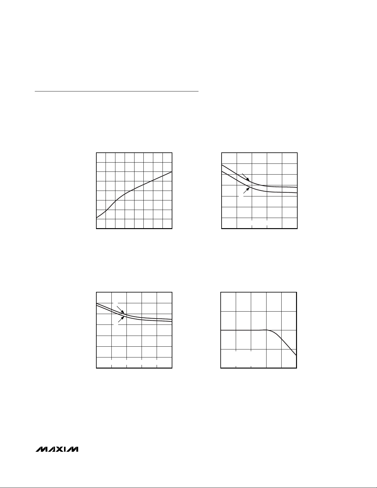
SUPPLY CURRENT vs. FREQUENCY
80
70
60
50
40
30
SUPPLY CURRENT (mA)
20
10
0
335
FREQUENCY (MHz)
MAX9218 toc01
31277 11 15 19 23
OUTPUT TRANSITION TIME
vs. OUTPUT SUPPLY VOLTAGE (V
7
6
t
5
4
3
2
OUTPUT TRANSITION TIME (ns)
1
0
1.8 3.3
R
t
F
RNG1 = RNG0 = HIGH
OUTPUT SUPPLY VOLTAGE (V)
)
CCO
MAX9218 toc02
3.02.72.42.1
OUTPUT TRANSITION TIME
vs. OUTPUT SUPPLY VOLTAGE (V
7
6
5
4
3
2
OUTPUT TRANSITION TIME (ns)
1
0
1.8 3.3
t
R
t
F
RNG1 = RNG0 = BOTH NOT HIGH
OUTPUT SUPPLY VOLTAGE (V)
)
CCO
MAX9218 toc03
3.02.72.42.1
-14
10
CAT5e
-13
10
-12
10
BIT-ERROR RATE
-11
10
-10
10
020
BIT-ERROR RATE
vs. CABLE LENGTH
35MHz CLOCK
700Mbps DATA RATE
FOR <12m, BER < 10
CAT5e CABLE LENGTH (m)
MAX9218 toc04
-12
161284
Page 6

MAX9218
27-Bit, 3MHz-to-35MHz
DC-Balanced LVDS Deserializer
6 _______________________________________________________________________________________
Pin Description
PIN NAME FUNCTION
Rising or Falling Latch Edge Select. LVTTL/LVCMOS input. Selects the edge of PCLK_OUT for
1R/F
latching data into the next chip. Set R/F = high for a rising latch edge. Set R/F = low for a falling latch
edge. Internally pulled down to GND.
2 RNG1
3V
4 IN+ Noninverting LVDS Serial Data Input
5 IN- Inverting LVDS Serial Data Input
6 LVDS GND LVDS Supply Ground
7 PLL GND PLL Supply Ground
8V
9 RNG0
10 GND Digital Supply Ground
11 V
12 REFCLK
13 PWRDWN LVTTL/LVCMOS Power-Down Input. Internally pulled down to GND.
14 OUTEN
15–23 CNTL_OUT [8:0]
CCLVDS
CCPLL
CC
LVTTL/LVCMOS Range Select Input. Set to the range that includes the serializer parallel clock input
frequency. Internally pulled down to GND.
LVDS Supply Voltage. Bypass to LVDS GND with 0.1µF and 0.001µF capacitors in parallel as close
to the device as possible, with the smallest value capacitor closest to the supply pin.
PLL Supply Voltage. Bypass to PLL GND with 0.1µF and 0.001µF capacitors in parallel as close to
the device as possible, with the smallest value capacitor closest to the supply pin.
LVTTL/LVCMOS Range Select Input. Set to the range that includes the serializer parallel clock input
frequency. Internal pulldown to GND.
Digital Supply Voltage. Supply for LVTTL/LVCMOS inputs and digital circuits. Bypass to GND with
0.1µF and 0.001µF capacitors in parallel as close to the device as possible, with the smallest value
capacitor closest to the supply pin.
LVTTL/LVCMOS Reference Clock Input. Apply a reference clock that is within ±2% of the serializer
PCLK_IN frequency. Internally pulled down to GND.
LVTTL/LVCMOS Output Enable Input. High activates the single-ended outputs. Driving low places
the single-ended outputs in high impedance. Internally pulled down to GND.
LVTTL/LVCMOS Control Data Outputs. CNTL_OUT[8:0] are latched into the next chip on the rising or
falling edge of PCLK_OUT as selected by R/F when DE_OUT is low, and are held at the last state
when DE_OUT is high.
24 DE_OUT
25, 37 V
26, 38 V
27 LOCK LVTTL/LVCMOS Lock Indicator Output. Outputs are valid when LOCK is low.
28 PCLK_OUT LVTTL/LVCMOS Parallel Clock Output. Latches data into the next chip on the edge selected by R/F.
29–36,
39–48
EP GND Exposed Pad for Thin QFN Package Only. Connect to GND.
RGB_OUT [17:0]
GND Output Supply Ground
CCO
CCO
LVTTL/LVCMOS Data Enable Output. High indicates RGB_OUT[17:0] are active. Low indicates
CNTL_OUT[8:0] are active.
Output Supply Voltage. Bypass to GND with 0.1µF and 0.001µF capacitors in parallel as close to the
device as possible, with the smallest value capacitor closest to the supply pin.
LVTTL/LVCMOS Red, Green, and Blue Digital Video Data Outputs. RGB_OUT[17:0] are latched into
the next chip on the edge of PCLK_OUT selected by R/F when DE_OUT is high, and are held at the
last state when DE_OUT is low.
Page 7

MAX9218
27-Bit, 3MHz-to-35MHz
DC-Balanced LVDS Deserializer
_______________________________________________________________________________________ 7
Functional Diagram
Figure 1. LVDS Input Bias
Figure 2. Worst-Case Output Pattern
Figure 3. Output Rise and Fall Times
Figure 4. High and Low Times
IN+
IN+
RNG0
RNG1
R/F
1
IN-
PLL
TIMING AND
CONTROL
DC BALANCE/
DECODE
SER-TO-PAR
0
OUTEN
RGB_OUT[17:0]
CNTL_OUT[8:0]
DE_OUT
PCLK_OUT
REFCLK
PWRDWN
LOCK
MAX9218
0.9V
0.1V
CCO
CCO
t
F
R
IB
1.2V
R
IB
LVDS
RECEIVER
DE_OUT
LOCK
PCLK_OUT
RGB_OUT[17:0]
CNTL_OUT[8:0]
t
R
IN-
PCLK_OUT
ODD
RGB_OUT
CNTL_OUT
EVEN
RGB_OUT
CNTL_OUT
RISING LATCH EDGE SHOWN (R/F = HIGH).
PCLK_OUT
t
LOW
t
HIGH
2.0V
0.8V
Page 8

MAX9218
27-Bit, 3MHz-to-35MHz
DC-Balanced LVDS Deserializer
8 _______________________________________________________________________________________
Figure 5. Synchronous Output Timing
Figure 6. Deserializer Delay
PCLK_OUT
PCLK_OUT SHOWN FOR R/F = HIGH (RISING LATCH EDGE)
DE_OUT
LOCK
RGB_OUT[17:0]
CNTL_OUT[8:0]
20 SERIAL BITS PCLK_OUT SHOWN FOR R/F = HIGH
IN+, IN-
SERIAL-WORD N SERIAL-WORD N + 1
0.8V
2.0V
0.8V
t
DVB
t
DVA
2.0V2.0V
0.8V
t
DELAY
PCLK_OUT
CNTL_OUT
RGB_OUT
PARALLEL-WORD N - 1 PARALLEL-WORD N
Page 9

MAX9218
27-Bit, 3MHz-to-35MHz
DC-Balanced LVDS Deserializer
_______________________________________________________________________________________ 9
PWRDWN
Figure 7. PLL Lock to REFCLK and Power-Down Delay
Figure 8. Output Enable Time
Figure 9. Output Disable Time
REFCLK
0.8V
2.0V
t
PLLREF
TRANSITION
WORD
FOUND
t
PDD
RECOVERED CLOCK
PCLK_OUT
RGB_OUT
CNTL_OUT
DE_OUT
LOCK
NOTE: R/F = HIGH
HIGH IMPEDANCE
HIGH IMPEDANCE
HIGH IMPEDANCE
OUTEN
0.8V
t
OE
DE_OUT
LOCK
RGB_OUT[17:0]
CNTL_OUT[8:0]
ACTIVEHIGH-Z
CLOCK STRETCH
OUTEN
DE_OUT
LOCK
RGB_OUT[17:0]
CNTL_OUT[8:0]
VALID DATA
2.0V
HIGH IMPEDANCE
HIGH IMPEDANCE
HIGH IMPEDANCE
t
OZ
HIGH-ZACTIVE
Page 10

MAX9218
27-Bit, 3MHz-to-35MHz
DC-Balanced LVDS Deserializer
10 ______________________________________________________________________________________
Detailed Description
The MAX9218 DC-balanced deserializer operates at a
parallel clock frequency of 3MHz to 35MHz, deserializing video data to the RGB_OUT[17:0] outputs when the
data enable output DE_OUT is high, or control data to
the CNTL_OUT[8:0] outputs when DE_OUT is low. The
video phase words are decoded using 2 overhead bits,
EN0 and EN1. Control phase words are decoded with 1
overhead bit, EN0. Encoding, performed by the
MAX9217 serializer, reduces EMI and maintains DC
balance across the serial cable. The serial input word
formats are shown in Table 1 and Table 2.
Control data inputs C0 to C4, each repeated over 3 serial bit times by the serializer, are decoded using majority
voting. Two or three bits at the same state determine the
state of the recovered bit, providing single bit-error tolerance for C0 to C4. The state of C5 to C8 is determined by the level of the bit itself (no voting is used).
AC-Coupling Benefits
AC-coupling increases the input voltage of the LVDS
receiver to the voltage rating of the capacitor. Two
capacitors are sufficient for isolation, but four capacitors—two at the serializer output and two at the deserializer input—provide protection if either end of the
cable is shorted to a high voltage. AC-coupling blocks
low-frequency ground shifts and common-mode noise.
The MAX9217 serializer can also be DC-coupled to the
MAX9218 deserializer. Figure 10 is the AC-coupled
serializer and deserializer with two capacitors per link,
and Figure 11 is the AC-coupled serializer and deserializer with four capacitors per link.
Applications Information
Selection of AC-Coupling Capacitors
See Figure 12 for calculating the capacitor values for
AC-coupling, depending on the parallel clock frequency. The plot shows capacitor values for two- and fourcapacitor-per-link systems. For applications using less
than 18MHz clock frequency, use 0.125µF capacitors.
Termination and Input Bias
The IN+ and IN- LVDS inputs are internally connected
to +1.2V through 35kΩ (min) to provide biasing for ACcoupling (Figure 1). Assuming 100Ω interconnect, the
LVDS input can be terminated with a 100Ω resistor.
Match the termination to the differential impedance of
the interconnect.
Use a Thevenin termination, providing 1.2V bias, on an
AC-coupled link in noisy environments. For interconnect with 100Ω differential impedance, pull each LVDS
line up to V
CC
with 130Ω and down to ground with 82Ω
at the deserializer input (Figure 10 and Figure 11). This
termination provides both differential and commonmode termination. The impedance of the Thevenin termination should be half the differential impedance of
the interconnect and provide a bias voltage of 1.2V.
Bit 0 is the LSB and is deserialized first. EN[1:0] are encoding bits. S[17:0] are encoded symbols.
Table 1. Serial Video Phase Word Format
Bit 0 is the LSB and is deserialized first. C[8:0] are the mapped control inputs.
Table 2. Serial Control Phase Word Format
0 1 2 3 4 5 6 7 8 9 10 11 12 13 14 15 16 17 18 19
EN0 EN1 S0 S1 S2 S3 S4 S5 S6 S7 S8 S9 S10 S11 S12 S13 S14 S15 S16 S17
012345678910111213141516171819
E N 0C0C0C0C1C1C1C2C2C2C3C3C3C4C4C4C5C6C7C8
Page 11

MAX9218
27-Bit, 3MHz-to-35MHz
DC-Balanced LVDS Deserializer
______________________________________________________________________________________ 11
Figure 10. AC-Coupled Serializer and Deserializer with Two Capacitors per Link
Figure 11. AC-Coupled Serializer and Deserializer with Four Capacitors per Link
V
CC
130Ω
RGB_IN
CNTL_IN
DE_IN
PCLK_IN
RNG0
RNG1
PWRDWN
1
0
INPUT LATCH
PLL
ENCODE
DC BALANCE/
TIMING AND
CONTROL
PAR-TO-SER
OUT
CMF
MOD0
MOD1
*
*
82Ω 82Ω
RNG0
RNG1
MAX9217
CERAMIC RF SURFACE-MOUNT CAPACITOR
130Ω
IN
PLL
TIMING AND
CONTROL
100Ω DIFFERENTIAL STP CABLE
*CAPS CAN BE AT EITHER END.
DECODE
DC BALANCE/
MAX9218
1
0
SER-TO-PAR
R/F
OUTEN
RGB_OUT
CNTL_OUT
DE_OUT
PCLK_OUT
REF_IN
PWRDWN
LOCK
V
CC
130Ω
RGB_IN
CNTL_IN
DE_IN
PCLK_IN
RNG0
RNG1
PWRDWN
1
0
INPUT LATCH
PLL
ENCODE
DC BALANCE/
TIMING AND
CONTROL
PAR-TO-SER
OUT
CMF
MOD0
MOD1
82Ω 82Ω
RNG0
RNG1
MAX9217
CERAMIC RF SURFACE-MOUNT CAPACITOR
130Ω
IN
PLL
TIMING AND
CONTROL
100Ω DIFFERENTIAL STP CABLE
DECODE
DC BALANCE/
MAX9218
1
0
SER-TO-PAR
R/F
OUTEN
RGB_OUT
CNTL_OUT
DE_OUT
PCLK_OUT
REF_IN
PWRDWN
LOCK
Page 12

MAX9218
27-Bit, 3MHz-to-35MHz
DC-Balanced LVDS Deserializer
12 ______________________________________________________________________________________
Input Frequency Detection
A frequency-detection circuit detects when the LVDS
input is not switching. When not switching, all outputs
except LOCK are low, LOCK is high, and PCLK_OUT
follows REFCLK. This condition occurs, for example, if
the serializer is not driving the interconnect or if the
interconnect is open.
Frequency Range Setting (RNG[1:0])
The RNG[1:0] inputs select the operating frequency
range of the MAX9218 and the transition time of the
outputs. Select the frequency range that includes the
MAX9217 serializer PCLK_IN frequency. Table 3 shows
the selectable frequency ranges and the corresponding data rates and output transition times.
Power Down
Driving PWRDWN low puts the outputs in high impedance and stops the PLL. With PWRDWN ≤ 0.3V and all
LVTTL/LVCMOS inputs ≤ 0.3V or ≥ VCC- 0.3V, the supply current is reduced to less than 50µA. Driving
PWRDWN high initiates lock to the local reference clock
(REFCLK) and afterwards to the serial input.
Lock and Loss of Lock (
LOCK
)
When PWRDWN is driven high, the PLL begins locking
to REFCLK, drives LOCK from high impedance to high
and the other outputs from high impedance to low
except PCLK_OUT. PCLK_OUT outputs REFCLK while
the PLL is locking to REFCLK. Locking to REFCLK
takes a maximum of 16,385 REFCLK cycles. When
locking to REFCLK is complete, the serial input is monitored for a transition word. When a transition word is
found, LOCK is driven low indicating valid output data,
and the parallel rate clock recovered from the serial
input is output on PCLK_OUT. PCLK_OUT is stretched
on the change from REFCLK to recovered clock (or
vice versa).
If a transition word is not detected within 220cycles of
PCLK_OUT, LOCK is driven high and the other outputs
except PCLK_OUT are driven low. REFCLK is output on
PCLK_OUT and the deserializer continues monitoring
the serial input for a transition word. See Figure 7 for
the synchronization timing diagram.
Output Enable (OUTEN) and
Busing Outputs
The outputs of two MAX9218s can be bused to form a
2:1 mux with the outputs controlled by the output
enable. Wait 30ns between disabling one deserializer
(driving OUTEN low) and enabling the second one (driving OUTEN high) to avoid contention of the bused outputs. OUTEN controls all outputs.
Rising or Falling Output Latch Edge (R/F)
The MAX9218 has a selectable rising or falling output
latch edge through a logic setting on R/F. Driving R/F
high selects the rising output latch edge, which latches
the parallel output data into the next chip on the rising
edge of PCLK_OUT. Driving R/F low selects the falling
output latch edge, which latches the parallel output
data into the next chip on the falling edge of
PCLK_OUT. The MAX9218 output-latch-edge polarity
does not need to match the MAX9217 serializer inputlatch-edge polarity. Select the latch-edge polarity
required by the chip being driven by the MAX9218.
Figure 12. AC-Coupling Capacitor Values vs. Clock Frequency
of 18MHz to 35MHz
Table 3. Frequency Range Programming
RNG1 RNG0
PARALLEL
CLOCK
(MHz)
00
01
1 0 7 to 15 140 to 300
1 1 15 to 35 300 to 700 Fast
3 to 7 60 to 140
SERIAL
DATA RATE
(Mbps)
OUTPUT
TRANSITION
TIME
Slow
AC-COUPLING CAPACITOR VALUE
vs. PARALLEL CLOCK FREQUENCY
140
125
110
95
80
65
CAPACITOR VALUE (nF)
50
35
20
18 36
FOUR CAPACITORS PER LINK
TWO CAPACITORS PER LINK
PARALLEL CLOCK FREQUENCY (MHz)
333021 24 27
Page 13

MAX9218
27-Bit, 3MHz-to-35MHz
DC-Balanced LVDS Deserializer
______________________________________________________________________________________ 13
Staggered and Transition Time Adjusted
Outputs
RGB_OUT[17:0] are grouped into three groups of six,
with each group switching about 1ns apart in the video
phase to reduce EMI and ground bounce.
CNTL_OUT[8:0] switch during the control phase. Output
transition times are slower in the 3MHz-to-7MHz and
7MHz-to-15MHz ranges and faster in the 15MHz-to35MHz range.
Data Enable Output (DE_OUT)
The MAX9218 deserializes video and control data at different times. Control data is deserialized during the video
blanking time. DE_OUT high indicates that video data is
being deserialized and output on RGB_OUT[17:0].
DE_OUT low indicates that control data is being deserialized and output on CNTL_OUT[8:0]. When outputs are
not being updated, the last data received is latched on
the outputs. Figure 13 shows the DE_OUT timing.
Power-Supply Circuits and Bypassing
There are separate on-chip power domains for digital
circuits and LVTTL/LVCMOS inputs (V
CC
supply and
GND), outputs (V
CCO
supply and V
CCO
GND), PLL
(V
CCPLL
supply and V
CCPLL
GND), and the LVDS input
(V
CCLVDS
supply and V
CCLVDS
GND). The grounds are
isolated by diode connections. Bypass each VCC,
V
CCO
, V
CCPLL
, and V
CCLVDS
pin with high-frequency,
surface-mount ceramic 0.1µF and 0.001µF capacitors
in parallel as close to the device as possible, with the
smallest value capacitor closest to the supply pin. The
outputs are powered from V
CCO
, which accepts a
1.71V to 3.6V supply, allowing direct interface to inputs
with 1.8V to 3.3V logic levels.
Cables and Connectors
Interconnect for LVDS typically has a differential
impedance of 100Ω. Use cables and connectors that
have matched differential impedance to minimize
impedance discontinuities.
Twisted-pair and shielded twisted-pair cables offer
superior signal quality compared to ribbon cable and
tend to generate less EMI due to magnetic field canceling effects. Balanced cables pick up noise as common
mode, which is rejected by the LVDS receiver.
Board Layout
Separate the LVTTL/LVCMOS outputs and LVDS inputs
to prevent crosstalk. A four-layer PC board with separate
layers for power, ground, and signals is recommended.
Figure 13. Output Timing
PCLK_OUT
CNTL_OUT
DE_OUT
RGB_OUT
CONTROL DATA
= OUTPUT DATA HELD
CONTROL DATAVIDEO DATA
PCLK_OUT TIMING SHOWN FOR R/F = HIGH (RISING OUTPUT LATCH EDGE)
Page 14

MAX9218
27-Bit, 3MHz-to-35MHz
DC-Balanced LVDS Deserializer
14 ______________________________________________________________________________________
ESD Protection
The MAX9218 ESD tolerance is rated for the Human
Body Model and ISO 10605. ISO 10605 specifies ESD
tolerance for electronic systems. The Human Body
Model discharge components are C
S
= 100pF and R
D
= 1.5kΩ (Figure 14). The ISO 10605 discharge components are CS= 330pF and RD= 2kΩ (Figure 15).
Chip Information
TRANSISTOR COUNT: 17,782
PROCESS: CMOS
Figure 14. Human Body ESD Test Circuit
Figure 15. ISO 10605 Contact Discharge ESD Test Circuit
R
D
1MΩ
1.5kΩ
CHARGE-CURRENT-
DC
LIMIT RESISTOR
100pF
HIGH-
VOLTAGE
SOURCE
C
S
DISCHARGE
RESISTANCE
STORAGE
CAPACITOR
DEVICE
UNDER
TEST
R
D
S
2kΩ
DISCHARGE
RESISTANCE
STORAGE
CAPACITOR
DEVICE
UNDER
TEST
50Ω TO 100Ω
CHARGE-CURRENT-
DC
LIMIT RESISTOR
C
330pF
HIGH-
VOLTAGE
SOURCE
Page 15

MAX9218
27-Bit, 3MHz-to-35MHz
DC-Balanced LVDS Deserializer
______________________________________________________________________________________ 15
Package Information
(The package drawing(s) in this data sheet may not reflect the most current specifications. For the latest package outline information
go to www.maxim-ic.com/packages
.)
32L/48L,TQFP.EPS
PACKAGE OUTLINE, 32/48L TQFP, 7x7x1.4mm
21-0054
1
E
2
PACKAGE OUTLINE, 32/48L TQFP, 7x7x1.4mm
21-0054
2
E
2
Page 16

MAX9218
27-Bit, 3MHz-to-35MHz
DC-Balanced LVDS Deserializer
Maxim cannot assume responsibility for use of any circuitry other than circuitry entirely embodied in a Maxim product. No circuit patent licenses are
implied. Maxim reserves the right to change the circuitry and specifications without notice at any time.
16 ____________________Maxim Integrated Products, 120 San Gabriel Drive, Sunnyvale, CA 94086 408-737-7600
© 2005 Maxim Integrated Products Printed USA is a registered trademark of Maxim Integrated Products, Inc.
Package Information (continued)
(The package drawing(s) in this data sheet may not reflect the most current specifications. For the latest package outline information
go to www.maxim-ic.com/packages
.)
PACKAGE OUTLINE, 48L THIN QFN
6x6x0.8mm BODY / 0.4mm LEAD PITCH
NOTE :
1. ALL DIMENSIONS ARE IN mm. ANGLES IN DEGREES.
2. COPLANARITY APPLIES TO THE EXPOSED PAD AS WELL AS THE TERMINALS. COPLANARITY SHALL NOT EXCEED 0.08mm.
3. WARPAGE SHALL NOT EXCEED 0.10 mm.
4. PACKAGE LENGTH / PACKAGE WIDTH ARE CONSIDERED AS SPECIAL CHARACTERISTIC. (S)
5. REFER TO JEDEC MO-220.
6. THE TERMINAL #1 IDENTIFIER AND TERMINAL NUMBERING CONVENTION SHALL CONFORM TO JESD 95-1 SPP-012.
DETAILS OF TERMINAL #1 IDENTIFIER ARE OPTIONAL, BUT MUST BE LOCATED WITHIN THE ZONE INDICATED.
THE TERMINAL #1 IDENTIFIER MAY BE EITHER A MOLD OR MARKED FEATURE.
7. ND AND NE REFER TO THE NUMBER OF TERMINALS ON EACH D AND E SIDE RESPECTIVELY.
21-0160
1
A
2
48L THIN QFN.EPS
S
A
A1
A2
b
D
e
E
k
k1
L
L1
N
ND
NE
COMMON DIMENSIONS
O
MIN. NOM. MAX.
S
L
BMY
0.700 0.750 0.800
0.000 -- -- 0.050
0.150 0.200 0.250
5.900 6.000 6.100
5.900 6.000 6.050
0.250 0.350 0.450
0.350 0.450 0.550
0.400 0.500 0.600
0.300 0.400 0.500
0.200 REF.
0.400 TYP.
48
12
12
PKG.
CODE
T4866-1
EXPOSED PAD VARIATONS
D2
MIN. NOM. MAX. MIN. NOM. MAX.
PACKAGE OUTLINE, 48L THIN QFN
6x6x0.8mm BODY / 0.4mm LEAD PITCH
E2
4.404.304.204.404.304.20
21-0160
2
A
2
 Loading...