

Page 1
General Description
The MAX9201/MAX9202/MAX9203 high-speed, lowpower, quad/dual/single comparators feature TTL logic
outputs with active internal pullups. Fast propagation
delay (7ns typ at 5mV overdrive) makes these devices
ideal for fast A/D converters and sampling circuits, line
receivers, V/F converters, and many other data-discrimination, signal restoration applications.
All comparators can be powered from separate analog
and digital power supplies or from a single combined
supply voltage. The analog input common-mode range
includes the negative rail, allowing ground sensing
when powered from a single supply. The MAX9201/
MAX9202/MAX9203 consume only 9mW per comparator when powered from a +5V supply.
The MAX9202/MAX9203 feature output latches with TTL
compatible inputs. The comparator output states are
held when the latch inputs are driven low. The
MAX9201 provides all the same features as the
MAX9202/MAX9203 with the exception of the latches.
The MAX9201/MAX9202/MAX9203 are lower power and
lower cost upgrades to the MAX901/MAX902/MAX903
offering a 50% power savings and smaller packaging.
________________________Applications
____________________________Features
♦ Fast 7ns Propagation Delay
♦ Low 9mW/Comparator Power Consumption
♦ Separate Analog and Digital Supplies
♦ Flexible Analog Supply: +5V to +10V or ±5V
♦ Input Voltage Range Includes
Negative Supply Rail
♦ TTL-Compatible Outputs
♦ TTL-Compatible Latch Inputs
(MAX9202/MAX9203)
♦ Available in Space-Saving Packages
8-Pin SOT23 (MAX9203)
14-Pin TSSOP (MAX9202)
16-Pin TSSOP (MAX9201)
MAX9201/MAX9202/MAX9203
Low-Cost, 7ns, Low-Power
Voltage Comparators
________________________________________________________________ Maxim Integrated Products 1
Pin Configurations
For price, delivery, and to place orders, please contact Maxim Distribution at 1-888-629-4642,
or visit Maxim’s website at www.maxim-ic.com.
PART TEMP RANGE PIN-PACKAGE
MAX9201EUE -40°C to +85°C 16 TSSOP
MAX9201ESE -40°C to +85°C 16 Narrow SO
MAX9202EUD -40°C to +85°C 14 TSSOP
MAX9202ESD -40°C to +85°C 14 Narrow SO
-40°C to +85°C 8 SOT23-8
MAX9203ESA -40°C to +85°C 8 Narrow SO
Ordering Information
High-Speed A/D
Converters
High-Speed V/F
Converters
Line Receivers
High-Speed Signal
Squaring/Restoration
Threshold Detectors
Input Trigger Circuitry
High-Speed Data
Sampling
PWM Circuits
19-1936; Rev 0; 1/01
TOP VIEW
1
INA- IND-
INA+
2
GND
3
MAX9201
4
OUTA
OUTB
5
V
6
EE
INB+
7
INB-
8
SO/TSSOP
16
15
IND+
14
V
OUTD
13
OUTC
12
V
11
10
INC+
9
INC-
INA-
INA+
GND
CC
OUTA
DD
N.C.
EE
1
2
3
4
5
6
7
MAX9202
SO/TSSOP
MAX9203EKA-T
V
14
CC
V
1
CC
13
N.C.
12
OUTB
11
LATCHBLATCHA
10
V
DD
9
INB+
8
INB-V
2
IN-
EE
MAX9203
3
4
SO
87V
6
5
OUTIN+
GND
LATCHV
V
GND
LATCH
1
DD
2
MAX9203
3
4
SOT23
DD
87V
6
5
CC
IN+OUT
IN-
V
EE
Page 2
MAX9201/MAX9202/MAX9203
Low Cost, 7ns, Low-Power
Voltage Comparators
2 _______________________________________________________________________________________
ABSOLUTE MAXIMUM RATINGS
ELECTRICAL CHARACTERISTICS
(VCC= +5V, VEE= -5V, VDD= +5V, GND = 0, VCM= 0, LATCH_ = logic high, TA= -40°C to +85°C. Typical values are at TA= +25°C,
unless otherwise noted.) (Note 1)
Stresses beyond those listed under “Absolute Maximum Ratings” may cause permanent damage to the device. These are stress ratings only, and functional operation of the device at these or any other conditions beyond those indicated in the operational sections of the specifications is not implied. Exposure
to absolute maximum rating conditions for extended periods may affect device reliability.
Analog Supply Voltage (V
CC
- VEE) .....................................+12V
Digital Supply Voltage (VDD) .................................................+7V
Differential Input Voltage..................(VEE- 0.3V) to (VCC+ 0.3V)
Common Mode Input Voltage ..........(VEE- 0.3V) to (VCC+ 0.3V)
Latch Input Voltage
(MAX9202/MAX9203 only) .....................-0.3V to (V
DD
+ 0.3V)
Output Short-Circuit Duration
To GND ......................................................................Continuous
To VDD..................................................................................1min
Continuous Power Dissipation (T
A
= +70°C)
8-Pin SOT23-8 (derate 9.1mW/°C above +70°C) ...727mW/°C
8-Pin SO (derate 5.9mW/°C above +70°C).............471mW/°C
14-Pin TSSOP (derate 9.1mW/°C above +70°C) ....727mW/°C
14-Pin SO (derate 8.3mW/°C above +70°C)...........667mW/°C
16-Pin TSSOP (derate 9.4mW/°C above +70°C) ....755mW/°C
16-Pin SO (derate 8.7mW/°C above +70°C)...........696mW/°C
Operating Temperature Range ...........................-45°C to +85°C
Junction Temperature......................................................+150°C
Storage Temperature Range ............................-65°C to +150°C
Lead Temperature (soldering, 10s) ................................+300°C
Analog Supply Voltage Range V
Digital Supply Voltage Range V
Input Offset Voltage V
Input Bias Current I
Input Offset Current I
Common-Mode Input Voltage
Range
Common-Mode Rejection
Ratio
Power-Supply Rejection Ratio PSRR Note 3
Output High Voltage V
Output Low Voltage V
Latch Input Threshold Voltage
High
Latch Input Threshold Voltage
Low
Latch Input Current High I
Latch Input Current Low I
Input Capacitance C
Differential Input Impedance R
Common-Mode Input
Impedance
Positive Analog Supply
Current
PARAMETER SYMBOL CONDITIONS MIN TYP MAX UNITS
- VEEReferenced to V
CC
Referenced to GND 4.75 5.25 V
DD
VCM = 0,
OS
B
OS
V
CM
CMRR
OH
OL
V
LH
V
LL
LH
LL
IN
IND
R
INCM
I
CC
= 1.4V
V
OUT
I
or I
IN+
IN-
VCM = 0,
= 1.4V
V
OUT
Note 2 V
- 5.1V < V
V
OU T
(V
IN+
(V
IN+
C M
= 1.4V
- V
IN-
- V
IN-
< +2.75V
) > 250mV, I
) < -250mV, I
Note 4 1.4 2 V
Note 4 0.8 1.4 V
VLH = 3.0V, Note 4 0.5 3 µA
VLL = 0.3V, Note 4 0.5 3 µA
Note 5
EE
4.75 10.5 V
TA = +25°C14
T
= -40°C to +85°C 7.5
A
TA = +25°C 1.25 5
TA = -40°C to +85°C 7.0
TA = +25°C 50 250
T
= -40°C to +85°C 450
A
V
EE
- 0.1
C C -
2.25
TA = +25°C 50 150
T
= -40°C to +85°C 250
A
TA = +25°C 50 150
T
= -40°C to +85°C 250
A
= 1mA 3.0 3.5 V
SOURCE
= 8mA 0.25 0.4 V
SINK
4pF
5MΩ
5.5 MΩ
MAX9201 4.7 7
MAX9202 2.5 4.0
MAX9203 1.3 2
mV
µA
nA
V
µV/V
µV/V
mA
Page 3
MAX9201/MAX9202/MAX9203
Low Cost, 7ns, Low-Power
Voltage Comparators
_______________________________________________________________________________________ 3
Note 1: All devices are 100% production tested at TA= +25°C. All temperature limits are guaranteed by design.
Note 2: Inferred by CMRR test.
Note 3: Tested for +4.75V < V
CC
< +5.25V, and -5.25V < VEE< -4.75V with VDD= +5V, although permissible analog power-supply
range is 4.75V < V
CC
< +10.5V for single supply operation with VEEgrounded.
Note 4: Specification does not apply to MAX9201.
Note 5: I
CC
tested for 4.75V < VCC< +10.5V with VEEgrounded. IEEtested for -5.25V < VEE< -4.75V with VCC= +5V. IDDtested for
+4.75V < V
DD
< +5.25V with all comparator outputs low, worst-case condition.
Note 6: Guaranteed by design. Times are for 100mV step inputs (see propagation delay characteristics in Figures 2 and 3)
Note 7: Maximum difference in propagation delay between two comparators in the MAX9201/MAX9202.
TIMING CHARACTERISTICS
(VCC= +5V, VEE= -5V, VDD= +5V, GND = 0, VCM= 0, LATCH_ = logic high, TA= -40°C to +85°C. Typical values are at
T
A
= +25°C, unless otherwise noted.) (Notes 1, 6)
ELECTRICAL CHARACTERISTICS (continued)
(VCC= +5V, VEE= -5V, VDD= +5V, GND = 0, VCM= 0, LATCH_ = logic high, TA= -40°C to +85°C. Typical values are at TA= +25°C,
unless otherwise noted.) (Note 1)
Negative Analog Supply
Current
Power Dissipation P
PARAMETER SYMBOL CONDITIONS MIN TYP MAX UNITS
MAX9201 3.4 5.0
I
DD
EE
Note 5
Note 5
= V
V
CC
D
V
EE
= 0V
DD
= +5V,
MAX9202 1.8 3.0
MAX9203 1.0 1.6
MAX9201 2 3.0
MAX9202 1 1.5Digital Supply Current I
MAX9203 0.5 0.8
MAX9201 33 44
MAX9202 17 24
MAX9203 9 13
mA
mA
mW
Input-to-Output High
Response Time
Input-to-Output Low
Response Time
Rise Time t
Fall Time t
Difference in Response Time
Between Outputs
Latch Disable to Output High
Delay
Latch Disable to Output Low
Delay
Minimum Setup Time t
Minimum Hold Time t
Minimum Latch Disable
Pulse Width
PARAMETER SYMBOL CONDITIONS MIN TYP MAX UNITS
VOD = 5mV,
t
PD+
C
= 15pF,
L
I
OUT
= 2mA
VOD = 5mV,
t
PD-
R
F
∆t
PD
t
+(D) Note 4 10 ns
PD
t
-(D) Note 4 10 ns
PD
S
N
t
(D) Note 4 8 ns
PW
= 15pF,
C
L
I
= 2mA
OUT
CL = 15pF,
= 2mA
I
OUT
CL = 15pF,
= 2mA
I
OUT
Note 7
Note 4 2 ns
Note 4 1 ns
TA = +25°C79
ns
T
= -40°C to +85°C12
A
TA = +25°C79
ns
T
= -40°C to +85°C12
A
T
= +25°C 2.0 ns
A
T
= +25°C 1.0 ns
A
TA = +25°C 0.5 1.5
T
= -40°C to +85°C 2.5
A
ns
Page 4

MAX9201/MAX9202/MAX9203
Low Cost, 7ns, Low-Power
Voltage Comparators
4 _______________________________________________________________________________________
Typical Operating Characteristics
(VCC= +5V, VEE= -5V, VDD= +5V, GND = 0, VCM= 0, LATCH_ = logic high, V
OUT
= 1.4V, TA= +25°C, unless otherwise noted.)
0.4
0.8
0.6
1.2
1.0
1.6
1.4
1.8
-40 10-15 356085
INPUT BIAS CURRENT vs. TEMPERATURE
MAX9201 toc02
TEMPERATURE (°C)
INPUT BIAS CURRENT (µA)
VCM = 0
INPUT OFFSET VOLTAGE vs. TEMPERATURE
1.5
1.0
0.5
0
-0.5
INPUT OFFSET VOLTAGE (mV)
-1.0
-1.5
-40 10-15 35 60 85
TEMPERATURE (°C)
MAX9201 toc01
OUTPUT HIGH VOLTAGE (VOH)
vs. LOAD CURRENT
4.0
3.8
3.6
3.4
TA = +25°C
3.2
OUTPUT HIGH VOLTAGE (V)
3.0
2.8
0462 8 10 12
LOAD CURRENT (mA)
TA = +85°C
TA = -40°C
MAX9201 toc03
OUTPUT LOW VOLTAGE (VOL)
vs. LOAD CURRENT
400
350
300
250
200
150
100
OUTPUT LOW VOLTAGE (mV)
50
0
TA = -40°C
TA = +25°C
TA = +85°C
042681012
LOAD CURRENT (mA)
MAX9201 toc04
ICC SUPPLY CURRENT (PER COMPARATOR)
1.6
1.5
1.4
1.3
1.2
1.1
SUPPLY CURRENT (mA)
CC
I
1.0
0.9
0.8
5678910
SUPPLY VOLTAGE
vs. V
CC
TA = +85°C
TA = +25°C
TA = -40°C
VCC SUPPLY VOLTAGE (V)
VEE = GND
MAX9201 toc05
RESPONSE TIME vs. INPUT OVERDRIVE
10.0
9.5
9.0
8.5
8.0
7.5
7.0
RESPONSE TIME (ns)
6.5
6.0
5.5
5.0
t
PD-
t
PD+
010152052530354540 50
INPUT OVERDRIVE (mV)
MAX9201 toc06
Page 5

MAX9201/MAX9202/MAX9203
Low Cost, 7ns, Low-Power
Voltage Comparators
_______________________________________________________________________________________ 5
Typical Operating Characteristics (continued)
(VCC= +5V, VEE= -5V, VDD= +5V, GND = 0, VCM= 0, LATCH_ = logic high, V
OUT
= 1.4V, TA= +25°C, unless otherwise noted.)
Pin Description
6.0
7.0
6.5
8.5
8.0
7.5
9.5
9.0
10.0
0304010 20 50 60 70 80 90
RESPONSE TIME vs. LOAD CAPACITANCE
(5mV OVERDRIVE, R
LOAD
= 2.4kΩ)
MAX9201 toc08
LOAD CAPACITANCE (pF)
RESPONSE TIME (ns)
t
PD-
t
PD+
6.5
7.0
6.8
7.5
7.3
7.8
8.0
-40-30-20-100 1020304050607080 90
RESPONSE TIME vs. TEMPERATURE
(5mV OVERDRIVE)
MAX9201 toc07
TEMPERATURE (°C)
RESPONSE TIME (ns)
t
PD-
t
PD+
MAX9201
MAX9202
PIN NAME FUNCTION
1, 8, 9,
16
2, 7, 10,
15
IN_+
3 GND Ground
4, 5, 12,
13
OUT_ Output (Channels A, B, C, D)
6V
11 V
14 V
PIN NAME FUNCTION
IN_-
Negative Input (Channels A, B, C,
D)
Positive Input (Channels A, B, C,
D)
EE
DD
CC
Negative Analog Supply and
Substrate
Positive Digital Supply
Positive Analog Supply
1, 8 IN_- Negative Input (Channels A, B)
2, 9 IN_+ Positive Input (Channels A, B)
3 GND Ground
4, 11 LATCH_ Latch Input (Channels A, B)
5, 12 OUT_ Output (Channels A, B)
6, 13 N.C. No Connection
7V
10 V
14 V
EE
DD
CC
Negative Analog Supply and
Substrate
Positive Digital Supply
Positive Analog Supply
Page 6

Applications Information
Circuit Layout
Because of the large gain-bandwidth transfer function
of the MAX9201/MAX9202/MAX9203 special precautions must be taken to realize their full high-speed
capability. A printed circuit board with a good, lowinductance ground plane is mandatory. All decoupling
capacitors (the small 100nF ceramic type is a good
choice) should be mounted as close as possible to the
power-supply pins. Separate decoupling capacitors for
analog VCCand for digital VDDare also recommended.
Close attention should be paid to the bandwidth of the
decoupling and terminating components. Short lead
lengths on the inputs and outputs are essential to avoid
unwanted parasitic feedback around the comparators.
Solder the device directly to the printed circuit board
instead of using a socket.
Input Slew-Rate Requirements
As with all high-speed comparators, the high gain-bandwidth product of the MAX9201/MAX9202/ MAX9203 can
create oscillation problems when the input traverses the
linear region. For clean output switching without oscillation or steps in the output waveform, the input must meet
minimum slew-rate requirements (0.5V/s typ). Oscillation
is largely a function of board layout and of coupled
source impedance and stray input capacitance. Both
poor layout and large source impedance will cause the
part to oscillate and increase the minimum slew-rate
requirement. In some applications, it may be helpful to
apply some positive feedback between the output and
positive input. This pushes the output through the transition region clearly, but applies a hysteresis in threshold
seen at the input terminals.
TTL Output and Latch Inputs
The comparator TTL output stages are optimized for
driving low-power Schottky TTL with a fan-out of four.
When the latch is connected to a logic high level or left
floating, the comparator is transparent and immediately
responds to changes at the input terminals. When the
latch is connected to a TTL low level, the comparator
output latches (in the same state) the instant that the
latch command is applied, and will not respond to subsequent changes at the input. No latch is provided on
the MAX9201.
6 _______________________________________________________________________________________
MAX9201/9202/9203
Low Cost, 7ns, Low-Power
Voltage Comparators
Pin Description (continued)
Typical Power-Supply Alternatives
Figure 1a. Separate Analog Supply,
Common Ground
Figure 1b. Single +5V Supply, Common
Ground
Figure 1c. Split ±5V Supply, Separate
Ground
MAX9203
PIN
SO SOT
18VCCPositive Analog Supply
2 7 IN+ Positive Input
3 6 IN- Negative Input
45V
5 4 LATCH Latch Input
6 3 GND Ground
7 2 OUT Output
81VDDPositive Digital Supply
NAME FUNCTION
EE
Negative Analog Supply and
Substrate
+10V
+5V
V
CC
V
DD
OUT
GND
V
EE
+5V
V
V
CC
V
DD
OUT
GND
EE
+5V
-5V
+5V
V
CC
V
DD
OUT
GND
V
EE
Page 7
_______________________________________________________________________________________ 7
MAX9201/9202/9203
Low Cost, 7ns, Low-Power
Voltage Comparators
Power Supplies
The MAX9201/MAX9202/MAX9203 can be powered
from separate analog and digital supplies or from a single +5V supply. The analog supply can range from +5V
to +10V with VEEgrounded for single-supply operation
(Figures 1a and 1b) or from a split ±5V supply (Figure
1c). The VDDdigital supply always requires +5V.
In high-speed, mixed-signal applications where a common ground is shared, a noisy digital environment can
adversely affect the analog input signal. When set up with
separate supplies, the MAX9201/MAX9202/MAX9203
isolate analog and digital signals by providing a separate
analog ground (V
EE
) and digital ground (GND).
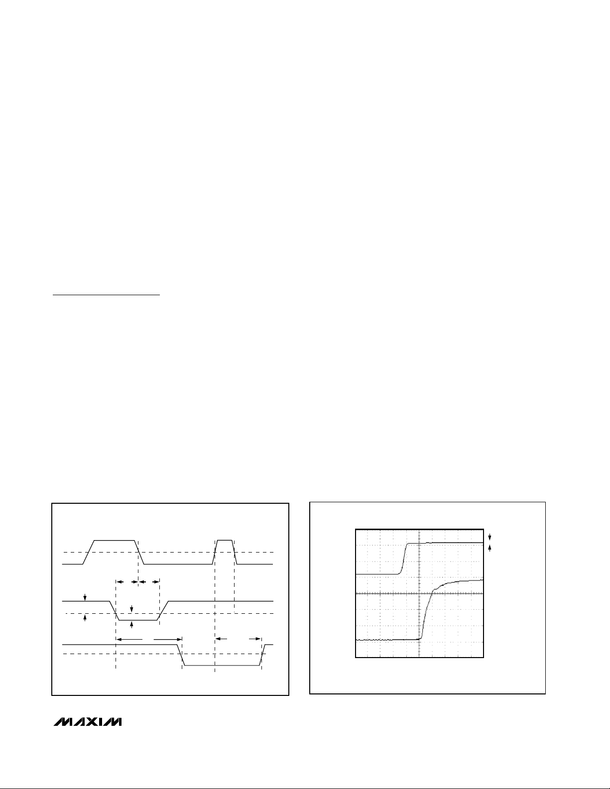
Definition of Terms
V
OS
Input Offset Voltage: Voltage applied be-
tween the two input terminals to obtain TTL
logic threshold (+1.4V) at the output.
V
IN
Input Voltage Pulse Amplitude: Usually set
to 100mV for comparator specifications.
V
OD
Input Voltage Overdrive: Usually set to 5mV
and in opposite polarity to VINfor comparator
specifications.
t
pd+
Input to Output High Delay: The propagation
delay measured from the time the input signal
crosses the input offset voltage to the TTL
logic threshold (+1.4V) of an output low to high
transition.
t
pd-
Input to Output Low Delay: The propagation
delay measured from the time the input signal
crosses the input offset voltage to the TTL
logic threshold (+1.4V) of an output high to low
transition.
t
pd+
(D) Latch Disable to Output High Delay: The
propagation delay measured from the latch
signal crossing the TTL logic threshold
(+1.4V) in a low to high transition to the point
of the output crossing TTL threshold (+1.4V)
in a low to high transition.
tpd- (D) Latch Disable to Output Low Delay: The
propagation delay measured from the latch
signal crossing the TTL threshold (+1.4V) in a
low to high transition to the point of the output
crossing TTL threshold (+1.4V) in a high to
low transition.
t
s
Minimum Setup Time: The minimum time,
before the negative transition of the latch signal, that an input signal change must be present in order to be acquired and held at the
outputs.
t
h
Minimum Hold Time: The minimum time,
after the negative transition of the latch signal, that an input signal must remain
unchanged in order to be acquired and held
at the output.
tpw(D) Minimum Latch Disable Pulse Width: The
minimum time that the latch signal must
remain high in order to acquire and hold an
input signal change.
Figure 2. MAX9201/MAX9202/MAX9203 Diagram Figure 3. t
PD+
Response Time to 5mV Overdrive
LATCH
ENABLE
INPUT
LATCH
COMPARATOR
V
IN
OUTPUT
COMPARE
LATCH
tst
h
V
OD
t
pd
COMPARE
tpw (D)
t
pd+
(D)
LATCH
1.4V
V
1.4V
INPUT
OS
OUTPUT
0V
0V
5ns/div
V
OD
50mV/div
1V/div
+ 5mV
Page 8

MAX9201/9202/9203
Low Cost, 7ns, Low-Power
Voltage Comparators
Figure 4. t
PD-
Response Time to 5mV Overdrive Figure 5. Response-Time Setup
Figure 6. Response to 50MHz Sine Wave
Figure 7. Response to 100MHz Sine Wave
Chip Information
MAX9201 TRANSISTOR COUNT: 348
MAX9202 TRANSISTOR COUNT: 176
MAX9203 TRANSISTOR COUNT: 116
PROCESS: Bipolar
Maxim cannot assume responsibility for use of any circuitry other than circuitry entirely embodied in a Maxim product. No circuit patent licenses are
implied. Maxim reserves the right to change the circuitry and specifications without notice at any time.
8 _____________________Maxim Integrated Products, 120 San Gabriel Drive, Sunnyvale, CA 94086 408-737-7600
© 2001 Maxim Integrated Products Printed USA is a registered trademark of Maxim Integrated Products.
INPUT
50mV/div
0V
OUTPUT
1V/div
0V
5ns/div
OUTPUT
0V
0V
INPUT
+ 5mV
V
OD
2V/div
10mV/div
INPUT TO 10X
SCOPE PROBE
(10MΩ 14pF)
PRECISION
STEP
GENERATOR
V
CC
OFFSET
ADJUST
OUTPUT
INPUT
= +5V VDD = +5V
V
CC
10kΩ
10kΩ
D.U.T.
V
EE
100nF
= -5V
1kΩ
10kΩ
100nF
0V
0V
100nF
R
L
2.43kΩ
OUTPUT TO 10X
SCOPE PROBE
(10MΩ 14pF)
100nF
2V/div
10mV/div
5ns/div
5ns/div
 Loading...