

Page 1
General Description
The MAX9132/MAX9134/MAX9135 high-speed, multiple-port, low-voltage differential signaling (LVDS) crossbar switches are specially designed for digital video
and camera signal transmission. These switches have a
wide bandwidth, supporting data rates up to 840Mbps.
The MAX9132 has three input ports and two output
ports, the MAX9134 has three input ports and four output ports, and the MAX9135 has four input ports and
three output ports. The digital video or camera signal
can go through the switches from an input port to one
or multiple output ports.
The MAX9132/MAX9134/MAX9135 switch routing is
programmable through either an I
2
C interface or a
Local Interconnect Network (LIN) serial interface. In
addition, the MAX9134/MAX9135 provide pins to set
switch routing. These pins also set the initial conditions
for the I2C mode. To generate more input or output
ports, these switches can be connected in parallel or in
cascade.
The MAX9132/MAX9134/MAX9135 operate from a
+3.3V supply and are specified over the -40°C to
+105°C temperature range. The MAX9134/MAX9135
are available in a 32-pin (5mm x 5mm) TQFP package,
while the MAX9132 is available in a 20-pin (6.5mm x
4.4mm) TSSOP package. The input/output port pins are
rated up to ±25kV ESD for the ISO Air-Gap Discharge
Model, ±15kV ESD for the IEC Air-Gap Discharge
Model, and ±10kV for the ESD Contact Discharge
Model. All other pins support up to ±3kV ESD for the
Human Body Model.
Applications
Digital Video in Automotive
Video/Audio Distribution Systems
Camera Surveillance Systems
High-Speed Digital Media Routing
Navigation System Displays
Features
Supports up to 840Mbps Data Rate at Each Port
Nonactivated Ports are in High-Impedance State
for Easy Port Expansion
Programmable Preemphasis on LVDS Outputs
Self Common-Mode Biasing on LVDS Inputs
Three Selectable Approaches for Switch Routing:
I
2
C Interface
LIN Interface
Programmable Pins (MAX9134/MAX9135)
> ±25kV ESD Protection
+3.3V Supply Voltage
-40°C to +105°C Operating Temperature Range
MAX9132/MAX9134/MAX9135
Programmable, High-Speed, Multiple
Input/Output LVDS Crossbar Switches
________________________________________________________________
Maxim Integrated Products
1
Pin Configurations
19-4215; Rev 0; 7/08
For pricing, delivery, and ordering information, please contact Maxim Direct at 1-888-629-4642,
or visit Maxim’s website at www.maxim-ic.com.
*
EP = Exposed pad.
+
Denotes a lead-free/RoHS-compliant package.
Note: Devices are specified over the -40°C to +105°C temperature range.
Pin Configurations continued at end of data sheet.
Ordering Information
PART PIN-PACKAGE INPUTS OUTPUTS ROUTE CONTROL
MAX9132GUP+ 20 TSSOP-EP* 3 2 I
2
C, LIN
MAX9134GHJ+ 32 TQFP-EP* 3 4 I2C, LIN, Pins
MAX9135GHJ+ 32 TQFP-EP* 4 3 I2C, LIN, Pins
20
19
18
17
16
15
14
13
1
2
3
4
5
6
7
8
SCL/RXD
LVDSVDD
DOUT0+DIN0-
DIN0+
DVDD
PD
TOP VIEW
DOUT0-
DOUT1+
DOUT1-
LVDSGNDDIN2-
DIN2+
DIN1-
DIN1+
12
11
9
10
AS1/NSLP
AS0
*EXPOSED PAD. CONNECT EP TO GND.
FS
AVDD
MAX9132
TSSOP-EP*
SDA/TXD
+
Page 2
MAX9132/MAX9134/MAX9135
Programmable, High-Speed, Multiple
Input/Output LVDS Crossbar Switches
2 _______________________________________________________________________________________
ABSOLUTE MAXIMUM RATINGS
DC ELECTRICAL CHARACTERISTICS
(V
AVDD
= V
DVDD
= V
LVDSVDD
= +3.0V to +3.6V, TA= -40°C to +105°C, unless otherwise noted. Typical values are at V
AVDD
= V
DVDD
= V
LVDSVDD
= +3.3V, TA= +25°C.) (Note 2)
Stresses beyond those listed under “Absolute Maximum Ratings” may cause permanent damage to the device. These are stress ratings only, and functional
operation of the device at these or any other conditions beyond those indicated in the operational sections of the specifications is not implied. Exposure to
absolute maximum rating conditions for extended periods may affect device reliability.
VDDto GND...........................................................-0.3V to +4.0V
All Pins to GND .............................................-0.3V to V
DD
+ 0.3V
Short-Circuit Duration (all outputs).............................Continuous
Continuous Power Dissipation (T
A
= +70°C)
32-Pin TQFP (derate 27.8mW/°C above +70°C)........2222mW
20-Pin TSSOP (derate 26.5mW/°C above +70°C) .....2122mW
Junction-to-Case Thermal Resistance (θ
JC
) (Note 1)
32-Pin TQFP ...................................................................4°C/W
20-Pin TSSOP.................................................................2°C/W
Junction-to-Ambient Thermal Resistance (θ
JA
) (Note 1)
32-Pin TQFP .................................................................36°C/W
20-Pin TSSOP............................................................37.7°C/W
Operating Temperature Range .........................-40°C to +105°C
Junction Temperature......................................................+150°C
Storage Temperature Range .............................-65°C to +150°C
ESD Protection
Human Body Model (RD= 1.5kΩ, CS= 100pF)
All Other Pins Including SCL, SDA to GND .................±2kV
IEC61000-4-2 (RD= 330Ω, CS= 150pF)
Contact Discharge
(DIN_, DOUT_) to GND ..............................................±10kV
Ai-Gap Discharge
(DIN_, DOUT_) to GND ..............................................±15kV
ISO10605 (RD= 2kΩ, CS= 330pF)
Contact Discharge
(DIN_, DOUT_) to GND ..............................................±10kV
Ai-Gap Discharge
(DIN_, DOUT_) to GND ..............................................±25kV
Lead Temperature (soldering, 10s) ................................+300°C
Note 1: Package thermal resistances were obtained using the method described in JEDEC specification JESD51-7, using a four-
layer board. For detailed information on package thermal considerations, refer to www.maxim-ic.com/thermal-tutorial
.
Supply Voltage V
Supply Current
SINGLE-ENDED CMOS INPUTS (PD, FS, RXD)
Input High Level V
Input Low Level V
Input High Current I
SINGLE-ENDED OUTPUTS (TXD, AS1/NSLP)
Output High Level V
Output Low Level V
3-LEVEL INPUTS (S5–S0, AS0, AS1)
Input High Level V
Input Low Level V
Input Open Level V
Input Current IL3, I
PARAMETER SYMBOL CONDITIONS MIN TYP MAX UNITS
DD
,
I
AVDD
I
DVDD
I
LVDSVDD
IH1
IL1
IN1
OH
OL
IH3
IL3
IO3
H3VIL3
Outputs switching at
,
20MHz
VIN = 0 to V
IOL = 4mA 0.4 V
Measured at the input pins 1.2 1.45 1.9 V
= 0 or V
DD
IH3
MAX9132 60 80
MAX9134/MAX9135 86 100
= V
DD
3.0 3.6 V
2.0 V
0.8 V
-20 +20 µA
VDD -
0.4
2.5 V
0.8 V
-20 +20 µA
mA
V
Page 3
MAX9132/MAX9134/MAX9135
Programmable, High-Speed, Multiple
Input/Output LVDS Crossbar Switches
_______________________________________________________________________________________ 3
,
DC ELECTRICAL CHARACTERISTICS (continued)
(V
AVDD
= V
DVDD
= V
LVDSVDD
= +3.0V to +3.6V, TA= -40°C to +105°C unless otherwise noted. Typical values are at V
AVDD
= V
DVDD
= V
LVDSVDD
= +3.3V, TA= +25°C.) (Note 2)
AC ELECTRICAL CHARACTERISTICS
(V
AVDD
= V
DVDD
= V
LVDSVDD
= +3.0V to +3.6V, TA= -40°C to +105°C, unless otherwise noted. Typical values are at V
AVDD
=
V
DVDD
= V
LVDSVDD
= +3.3V, TA= +25°C.) (Notes 3, 4)
DIFFERENTIAL INPUTS (DIN_)
Differential Input High Threshold V
Differential Input Low Threshold V
Common Input Voltage V
Input Current I
DIFFERENTIAL OUTPUTS (DOUT_)
Differential Output Voltage V
Change in VOD Between
Complementary Output States
Output Common-Mode Voltage V
Change in V
Complementary Output States
Output Short-Circuit Current I
SERIAL-INTERFACE INPUT, OUTPUT (SCL, SDA)
Input High Level V
Input Low Level V
H i g h- Level Outp ut Leakag e C ur r ent I
Low-Level Output V
Input Capacitance C
PARAMETER SYMBOL CONDITIONS MIN TYP MAX UNITS
COM
Between
VID = V
VID = V
V
COM
I
IN-
50Ω load, no preemphasis 250 3.65 450 mV
|0135mV
OD
4
|
Two output pins connected to GND -15 -7 mA
IH
IL
Open drain with 1kΩ pullup to V
IOL = 3mA 0.4 V
I
IN+
|∆V
|∆V
LEAKH
IDH
IDL
COM
OD
COM
COM
OS
OL
IN+
IN+
= (V
- V
- V
IN+
IN-
IN-
- V
)/2 1.00 1.29 1.60 V
IN-
DD
100 mV
-100 mV
-50 +50 µA
1.125 1.29 1.475 V
0135mV
0.7 x
V
DD
0.3 x
V
DD
V
V
1µA
10 pF
DIFFERENTIAL SIGNALS (DOUT_)
Output-to-Output Skew t
Rise Time t
Fall Time t
Duty Cycle D
PARAMETER SYMBOL CONDITIONS MIN TYP MAX UNITS
SK
RL = 100Ω differential 50 250 ps
20% to 80% of the signal swing; RL = 50Ω
R
differential (R
= 5pF
C
L
= 100Ω double termination),
L
0.3 0.4 ns
20% to 80% of the signal swing; RL = 50Ω
differential (R
F
C
= 5pF
L
Input duty cycle 50%; 840Mbps clock
pattern
= 100Ω double termination),
L
0.3 0.4 ns
45 55 %
Page 4
MAX9132/MAX9134/MAX9135
Programmable, High-Speed, Multiple
Input/Output LVDS Crossbar Switches
4 _______________________________________________________________________________________
Note 2: Parameters are 100% production tested at TA= +25°C, unless otherwise noted.
Note 3: I
2
C timing parameters are specified for fast-mode I2C. Maximum data rate = 400kbps.
Note 4: Parameters are guaranteed by design.
AC ELECTRICAL CHARACTERISTICS (continued)
(V
AVDD
= V
DVDD
= V
LVDSVDD
= +3.0V to +3.6V, TA= -40°C to +105°C, unless otherwise noted. Typical values are at V
AVDD
=
V
DVDD
= V
LVDSVDD
= +3.3V, TA= +25°C.) (Notes 3, 4)
Output Peak-to-Peak Jitter
(Pr eem p hasi s O n)
Propagation Delay t
LVDS Switchover Time t
LV D S w i th P r eem p hasi s Am p l i tud e|V
I2C TIMING
CLK Frequency f
Start Condition Hold Time t
Low Period of SCL Clock t
High Period of SCL Clock t
Repeated START Condition
Setup Time
Data Hold Time t
Data Setup Time t
Setup Time for STOP Condition t
Bus Free Time t
PARAMETER SYMBOL CONDITIONS MIN TYP MAX UNITS
t
J
D
LON
ODPE
SCL
HD:STA
LOW
HIGH
t
SU:STA
HD:DAT
SU:STA
SU:STO
BUF
VID = 200mV, V
pattern; input transition time (20% to 80%) =
200ps
VID = 200mV, V
23
- 1 PRBS pattern; input transition time
2
(20% to 80%) = 200ps
S w i tchover ti m e fr om one channel to another 100 ns
50Ω differential (100Ω double termination)
|
load, 840Mbps
(Figure 1) 0.6 µs
(Figure 1) 1.3 µs
(Figure 1) 0.6 µs
(Figure 1) 0.6 µs
(Figure 1) 0 0.9 µs
(Figure 1) 100 ns
(Figure 1) 0.6 µs
(Figure 1) 1.3 µs
= 1.2V, 840Mbps clock
COM
= 1.2V, 840Mbps
COM
10 30 ps
85 180 ps
2ns
335 530 680 mV
400 kHz
Page 5
MAX9132/MAX9134/MAX9135
Programmable, High-Speed, Multiple
Input/Output LVDS Crossbar Switches
_______________________________________________________________________________________
5
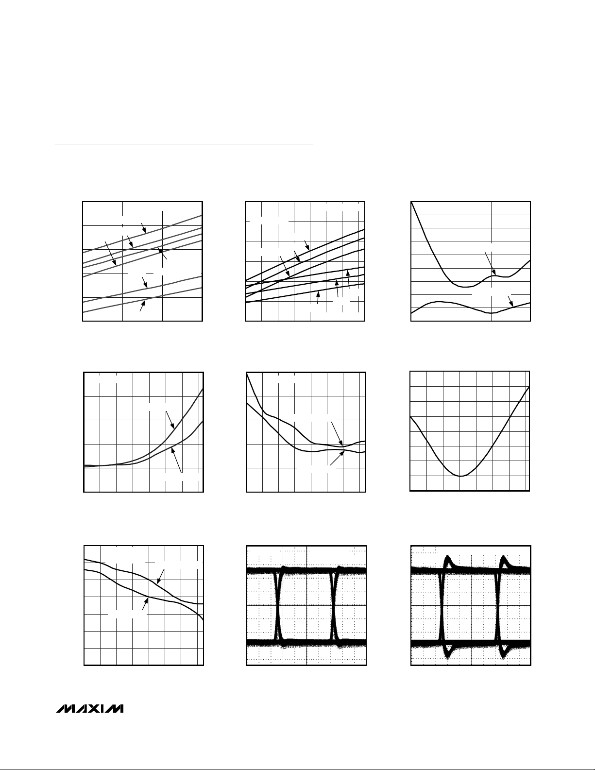
Typical Operating Characteristics
(V
AVDD
= V
DVDD
= V
LVDSVDD
= +3.3V, TA = +25°C, unless otherwise noted.)
SUPPLY CURRENT vs. SUPPLY VOLTAGE
105
PREEMPHASIS
100
+105°C
95
90
SUPPLY CURRENT (mA)
85
80
3.0 3.43.2 3.6
840Mbps 1010 PATTERN
-40°C
+25°C
+25°C
+105°C
SUPPLY VOLTAGE (V)
PEAK-TO-PEAK JITTER
vs. TEMPERATURE
250
840Mbps PRBS
200
NO PREEMPHASIS
150
100
PEAK-TO-PEAK JITTER (ps)
50
0
-40 0 20-20 40 60 80 100
TEMPERATURE (°C)
SUPPLY CURRENT vs. DATA RATE
105
PREEMPHASIS
100
-40°C
NO PREEMPHASIS
PREEMPHASIS
MAX9132/4/5 toc01
95
90
85
SUPPLY CURRENT (mA)
80
75
100 300200 400 500 600 700 800
250
200
MAX9132/4/5 toc04
150
100
PEAK-TO-PEAK JITTER (ps)
50
0
100 300 400200 500 600 700 800
-40°C
+25°C
+105°C
+105°C
DATA RATE (Mbps)
PEAK-TO-PEAK JITTER
vs. DATA RATE
PRBS PATTERN
NO PREEMPHASIS
PREEMPHASIS
DATA RATE (Mbps)
1010 PATTERN
-40°C
+25°C
NO PREEMPHASIS
130
125
120
MAX9132/4/5 toc02
115
110
105
100
PEAK-TO-PEAK JITTER (ps)
95
90
85
3.0 3.2 3.4 3.6
CHANNEL-TO-CHANNEL SKEW
45
46
47
MAX9132/4/5 toc05
48
49
50
51
CHANNEL-TO-CHANNEL SKEW (ps)
52
53
-40 0 20-20 40 60 80 100
PEAK-TO-PEAK JITTER
vs. SUPPLY VOLTAGE
840Mbps PRBS
MAX9132/4/5 toc03
NO PREEMPHASIS
PREEMPHASIS
SUPPLY VOLTAGE (V)
vs. TEMPERATURE
MAX9132/4/5 toc06
TEMPERATURE (°C)
CHANNEL-TO-CHANNEL SKEW
vs. DATA RATE
35
30
25
20
15
10
CHANNEL-TO-CHANNEL SKEW (ps)
5
0
1010 PATTERN
= 200mV
V
DIFF
PREEMPHASIS
100 300 400200 500 600 700 800
DATA RATE (Mbps)
NO PREEMPHASIS
MAX9132/4/5 toc07
OV
150mV/div
EYE DIAGRAM
200Mbps PRBS
NO PREEMPHASIS
1ns/div
MAX9132/4/5 toc08
EYE DIAGRAM
200Mbps PRBS WITH PREEMPHASIS
150mV/div
MAX9132/4/5 toc09
OV
1ns/div
Page 6
Pin Description
MAX9132/MAX9134/MAX9135
Programmable, High-Speed, Multiple
Input/Output LVDS Crossbar Switches
6 _______________________________________________________________________________________
Typical Operating Characteristics (continued)
(V
AVDD
= V
DVDD
= V
LVDSVDD
= +3.3V, TA = +25°C, unless otherwise noted.)
OV
200ps/div
EYE DIAGRAM
MAX9132/4/5 toc10
150mV/div
840Mbps PRBS
NO PREEMPHASIS
OV
200ps/div
EYE DIAGRAM
MAX9132/4/5 toc11
150mV/div
840Mbps PRBS WITH PREEMPHASIS
MAX9132
TSSOP
13130PD
23231DVDD
3 1 1 DIN0+ Port 0 Positive Input
4 2 2 DIN0- Port 0 Negative Input
5 3 3 DIN1+ Port 1 Positive Input
6 4 4 DIN1- Port 1 Negative Input
— 5 — AGND Analog Ground
7 6 5 DIN2+ Port 2 Positive Input
8 7 6 DIN2- Port 2 Negative Input
— — 7 DIN3+ Port 3 Positive Input
— — 8 DIN3- Port 3 Negative Input
989AVDD
10——FSI
— 9 10 S0 Routing Selection 0 Input. See Tables 6a and 6b.
— 10 11 S1 Routing Selection 1 Input. See Tables 6a and 6b.
— 11 12 S2 Routing Selection 2 Input. See Tables 6a and 6b.
— 12 13 S3 Routing Selection 3 Input. See Tables 6a and 6b.
11 13 14 AS0
MAX9134
TQFP
PIN
MAX9135
TQFP
NAME FUNCTION
P ow er - D ow n Inp ut. P D = l ow for p ow er - d ow n. P D = hi g h for p ow er - up w i thout
p r eem p hasi s. Leave P D op en for p ow er - up w i th p r eem p hasi s on al l outp uts.
Digital Power Supply. Bypass DVDD to DGND with 0.1µF and 0.01µF
capacitors as close as possible to the device.
Analog Power Supply. Bypass AVDD to AGND with 0.1µF and 0.01µF
capacitors as close as possible to the device.
2
C and LIN Interface Selection Input. FS = low for LIN, FS = high for I2C.
3-Level I
Input (Table 4)
2
C Address Selection 0 Input (Table 3) or LIN Identifier Selection 0
Page 7

MAX9132/MAX9134/MAX9135
Programmable, High-Speed, Multiple
Input/Output LVDS Crossbar Switches
_______________________________________________________________________________________ 7
Pin Description (continued)
PIN
MAX9132
TSSOP
12 14 15 AS1/NSLP
13 16, 25 19, 24 LVDSGND LVDS Ground
— 17 — DOUT3- Port 3 Negative Output
— 18 — DOUT3+ Port 3 Positive Output
— 19 17 DOUT2- Port 2 Negative Output
— 20 18 DOUT2+ Port 2 Positive Output
14 21 20 DOUT1- Port 1 Negative Output
15 22 21 DOUT1+ Port 1 Positive Output
16 23 22 DOUT0- Port 0 Negative Output
17 24 23 DOUT0+ Port 0 Positive Output
18 15, 26 16, 25 LVDSVDD
19 27 26 SDA/TXD
20 28 27 SCL/RXD
— 29 28 S5 Routing Selection 5 Input. See Tables 6a and 6b.
— 30 29 S4 Routing Selection 4 Input. See Tables 6a and 6b.
— — 32 DGND Digital Ground
———EP
MAX9134
TQFP
MAX9135
TQFP
NAME FUNCTION
2
3-Level I
mode, it becomes an NSLP output, the sleep mode activation pin (active
low) to the LIN bus driver.
LVDS Supply Input. Bypass LVDSVDD to LVDSGND with 0.1µF and 0.01µF
capacitors as close as possible to the device.
2
I
mode and TXD when in LIN mode.
2
I
when in LIN mode.
Exposed Pad. Internally connected to GND. Connect to a large ground
plane to maximize thermal performance.
C Address Selection 1 Input (in I2C Mode, Table 3). In LIN bus
C Data Link Input/LIN Tx Output. SDA/TXD becomes SDA when in I2C
C Clock/LIN Rx Input. SCL/RXD becomes SCL when in I2C mode and RXD
Page 8

MAX9132/MAX9134/MAX9135
Programmable, High-Speed, Multiple
Input/Output LVDS Crossbar Switches
8 _______________________________________________________________________________________
Functional Diagrams
DVDD
DGND
AVDD
AGND
LVDSVDD
LVDSGND
DIN0+ DIN1+
DIN0- DIN1-
DOUT0- DOUT1-
DOUT1+
DIN2+
DIN2- FS
MAX9132
ROUTING
CONTROL
REGISTERS
2
I
C/LIN
INTERFACE
AS1/
AS0DOUT0+
NSLP
DIN0+ DIN1+
DIN0- DIN1-
PD
SCL/RXD
SDA/TXD
DIN2+
DIN2-
DVDD
DGND
AVDD
AGND
LVDSVDD
LVDSGND
DIN3+
DIN3- S5
DVDD
DGND
AVDD
AGND
LVDSVDD
LVDSGND
DOUT0+
DOUT0-
ROUTING
CONTROL
REGISTERS
INTERFACE
DIN0+ DIN1+
DIN0- DIN1-
DOUT1- DOUT2-
S4S3S2S1S0
2
I
C/LIN
DOUT2+
PD
SCL/RXD
SDA/TXD
DIN2+
DIN2- S5
MAX9134
DOUT3+
DOUT3-
ROUTING
CONTROL
REGISTERS
I
INTERFACE
AS0DOUT1+
2
C/LIN
S4S3S2S1S0
PD
SCL/RXD
SDA/TXD
AS1/
NSLP
MAX9135
DOUT0+
DOUT0-
DOUT2+
DOUT1- DOUT2-
AS1/
AS0DOUT1+
NSLP
Page 9

MAX9132/MAX9134/MAX9135
Programmable, High-Speed, Multiple
Input/Output LVDS Crossbar Switches
_______________________________________________________________________________________ 9
Detailed Description
The MAX9132/MAX9134/MAX9135 high-speed, multiple-port, low-voltage differential signaling (LVDS)
crossbar switches are specially designed for digital
video and camera signal transmission. These switches
have a wide bandwidth, supporting data rates up to
840Mbps. This allows the use of MAX9132/MAX9134/
MAX9135 with LVDS serializers/deserializers (SerDes)
to create a complete video or camera network. The
MAX9132 has three input ports and two output ports,
the MAX9134 has three input ports and four output
ports, and the MAX9135 has four input ports and three
output ports. The video or camera signal can go
through the switch from an input port to one or multiple
output ports.
The MAX9132/MAX9134/MAX9135 switch routing is
programmable through either an I2C interface or a
Local Interconnect Network (LIN) serial interface. AS0
and AS1 set the slave addresses for either of these
modes, allowing several devices on a bus simultaneously. In addition, the MAX9134/MAX9135 provide
3-level pins S[5:0] to set switch routing and the initial
conditions for I2C mode. To improve the signal integrity,
all the LVDS outputs feature selectable preemphasis.
Initial Power-Up
On power-up, all control registers have a value of 0x00.
For the MAX9134/MAX9135, leaving S[5:0] unconnected, allows control through the LIN interface with all outputs deactivated. Otherwise, the switch runs in
pin-control mode with S[5:0] controlling the switch routing. The I2C is also active while the device is in pincontrol mode. Successful routing through I2C overrides
the pin settings. For more details, see the
I2C Interface
section. For the MAX9132, the FS input determines
which interface is active.
Register Description
There are four 1-byte control registers in the
MAX9132/MAX9134/MAX9135. These registers control
the routing of the switch. Table 1 describes the register
map for both I
2
C and LIN. When the MAX9132/
MAX9134/MAX9135 operate in LIN mode, register 0x00
acts as an error flag register. Its function is described
in detail in Table 5. In either I
2
C or LIN mode, the control registers (0x01, 0x02) program the MAX9132/
MAX9134/MAX9135 switch routing control. In addition,
these registers can individually activate and deactivate
preemphasis for each output port. Table 2a describes
the routing for the MAX9132/MAX9134 and Table 2b for
the MAX9135. For I2C programming, register 0xFF controls the activation of routing.
SDA
SCL
t
HD:STA
t
LOW
t
HIGH
t
R
t
F
t
SU:DAT
t
SU:STA
t
SU:STO
t
BUF
t
HD:STA
t
HD:DAT
START
CONDITION
STOP
CONDITION
START
CONDITION
REPEATED
START CONDITION
Figure 1. I2C Serial-Interface Timing Details
Table 1. Register Address Map
REGISTER
ADDRESS (HEX)
0x00 R LIN Status Register Reserved
0x01 R/W Switch Control Register 1 Switch Control Register 1
0x02 R/W
0xFF W Reserved Route Activation Register
READ/
WRITE
LIN INTERFACE DESCRIPTION I
Switch Control Register 2 (MAX9134/MAX9135
only)
2
C DESCRIPTION
Switch Control Register 2 (MAX9134/MAX9135
only)
Page 10

MAX9132/MAX9134/MAX9135
Programmable, High-Speed, Multiple
Input/Output LVDS Crossbar Switches
10 ______________________________________________________________________________________
Table 2a. I2C/LIN Switch Routing Control Registers for the MAX9132/MAX9134
BIT 7…………….……………… BIT 0 ACK BIT BIT 7…………….…………………BIT 0 ACK BIT
8-BIT DATA AS
BIT 7…….…….…………BIT 0 ACK BIT
7-BIT SLAVE ID 0 AS
ADDR
AS
ADDRESS/COMMAND BYTE
S P
SINGLE WRITE
SINGLE READ
BIT 7…………….……….BIT 0 ACK BIT
BIT 7………….…………BIT 0 ACK BITBIT 7…………….……………BIT 0 ACK BIT
8-BIT DATA
/AM
BIT 7…….…………BIT 0 ACK BIT
7-BIT SLAVE ID
0AS
ADDR
AS S 7-BIT SLAVE ID
1AS
ADDRESS/COMMAND BYTE
S P
ADDR: 8-BIT REGISTER ADDRESS
S: 2-WIRE BUS START CONDITION BY MASTER
P: 2-WIRE BUS STOP CONDITION BY MASTER
AS: ACKNOWLEDGE BY SLAVE
AM: ACKNOWLEDGE BY MASTER
/AM: NO ACKNOWLEDGE BY MASTER
Figure 2. Single-Byte Write and Single-Byte Read
REGISTER
ADDRESS
0x01
0x02
(MAX9134 only)
REGISTER BIT(S) DESCRIPTION VALUE FUNCTION
D7 DOUT1 Preemphasis
0 DOUT1 preemphasis off
1 DOUT1 preemphasis on
000 DOUT1 in high impedance
D[6:4]
DOUT1 Routing
Connection
001 DOUT1 connected to DIN1
010 DOUT1 connected to DIN0
011 DOUT1 connected to DIN2
D3 DOUT0 Preemphasis
0 DOUT0 preemphasis off
1 DOUT0 preemphasis on
000 DOUT0 in high impedance
D[2:0]
DOUT0 Routing
Connection
001 DOUT0 connected to DIN1
010 DOUT0 connected to DIN0
011 DOUT0 connected to DIN2
D7 DOUT3 Preemphasis
0 DOUT3 preemphasis off
1 DOUT3 preemphasis on
000 DOUT3 in high impedance
D[6:4]
DOUT3 Routing
Connection
001 DOUT3 connected to DIN1
010 DOUT3 connected to DIN0
011 DOUT3 connected to DIN2
D3 DOUT2 Preemphasis
0 DOUT2 preemphasis off
1 DOUT2 preemphasis on
000 DOUT2 in high impedance
D[2:0]
DOUT2 Routing
Connection
001 DOUT2 connected to DIN1
010 DOUT2 connected to DIN0
011 DOUT2 connected to DIN2
Page 11

MAX9132/MAX9134/MAX9135
I2C Interface
The MAX9132/MAX9134/MAX9135 operate as slaves
that send and receive data through I
2
C (see Figure 1).
The interface uses a serial-data line (SDA) and a serialclock line (SCL) to achieve bidirectional communication
between master(s) and slave(s). A master (typically a
microcontroller) initiates all data transfers to and from
the slave and generates the SCL clock that synchronizes the data transfer. The SDA line operates as both
an input and an open-drain output. A pullup resistor,
typically 4.7kΩ, is required on SDA. The SCL line operates only as an input. A pullup resistor is required on
SCL if there are multiple masters on the I2C interface, or
if the master in a single-master system has an opendrain SCL output. Each transmission consists of a
START condition sent by a master, followed by the 7-bit
slave address plus R/W bit, a register address byte, a
data byte, and finally a STOP condition. Table 3 shows
the slave address selection by the AS0 and AS1 pins.
Data Format for Writing to the Slave
A write to the MAX9132/MAX9134/MAX9135 comprises
the transmission of the slave address with the R/W bit
set to 0, followed by at least 1 byte of information. The
first byte of information is the command byte. The command byte determines which registers of the
MAX9132/MAX9134/MAX9135 are to be written by the
next byte, if received. If a STOP condition is detected
after the command byte is received, the MAX9132/
MAX9134/MAX9135 take no further action beyond storing the command byte. Any bytes that are received
after the command byte are data bytes. The first data
byte goes into the internal register of the crossbar
switch selected by the command byte (Figure 2). If
Programmable, High-Speed, Multiple
Input/Output LVDS Crossbar Switches
______________________________________________________________________________________ 11
Table 2b. I2C Switch Routing Control Registers for the MAX9135
REGISTER
ADDRESS
0x01
0x02
REGISTER BIT(S) DESCRIPTION VALUE FUNCTION
D7 DOUT1 Preemphasis
D[6:4]
D3 DOUT0 Preemphasis
D[2:0]
D[7:4] Reserved 0000 Set these bits to 0000
D3 DOUT2 Preemphasis
D[2:0]
DOUT1 Routing
Connection
DOUT0 Routing
Connection
DOUT2 Routing
Connection
0 DOUT1 preemphasis off
1 DOUT1 preemphasis on
000 DOUT1 not connected
001 DOUT1 connected to DIN1
010 DOUT1 connected to DIN0
011 DOUT1 connected to DIN2
100 DOUT1 connected to DIN3
0 DOUT0 preemphasis off
1 DOUT0 preemphasis on
000 DOUT0 not connected
001 DOUT0 connected to DIN1
010 DOUT0 connected to DIN0
011 DOUT0 connected to DIN2
100 DOUT0 connected to DIN3
0 DOUT2 preemphasis off
1 DOUT2 preemphasis on
000 DOUT2 not connected
001 DOUT2 connected to DIN1
010 DOUT2 connected to DIN0
011 DOUT2 connected to DIN2
100 DOUT2 connected to DIN3
Page 12

MAX9132/MAX9134/MAX9135
Programmable, High-Speed, Multiple
Input/Output LVDS Crossbar Switches
12 ______________________________________________________________________________________
multiple data bytes are transmitted before a STOP condition is detected, these bytes are generally stored in
subsequent MAX9132/MAX9134/MAX9135 internal registers because the command byte address generally
autoincrements (Table 1).
Data Format for Reading from the Slave
The MAX9132/MAX9134/MAX9135 are read using the
devices’ internally stored command bytes as an
address pointer, the same way the stored command
byte is used as an address pointer for a write. The
pointer does not autoincrement after each data byte is
read. Initiate a read by writing the command byte to the
proper slave address (Figure 2), then send the device’s
slave address with the R/W bit set to 1. The slave now
responds with the contents of the requested register
(Figure 2).
LIN Interface
The LIN interface is a low-speed, low-cost interface used
in slow control signal traffic in automotive applications.
This device is the slave node in the LIN bus cluster and
is designed based on the LIN Rev. 1.3 specification. The
LIN master sends data to the MAX9132/MAX9134/
FRAME SLOT
FRAME
RESPONSE
SPACE
INTER-
FRAME
SPACE
RESPONSEHEADER
BREAK SYNC PROTECTED
INDENTIFIER
TRANSMITTED
FROM MASTER
TRANSMITTED
FROM A MASTER OR SLAVE
*N = 2 FOR WRITE
AND 4 FOR READ
DATA 1 DATA 2 DATA N* CHECKSUM
Figure 3. LIN Bus Signal Format
READ FORMATWRITE FORMAT
0x00 0x010x01
DATA 1 DATA 2 DATA 1 DATA 2 DATA 3 DATA 4
0x02 0x02 0xFF
Figure 4. LIN Write and Read Data Frame
Table 3. I2C Slave Addresses
PIN ADDRESS
AS0 AS1 A[7:5] A4 A3 A2 A1 A0
Low Low 101 0 0 0 0 R/W 0xA0
Low Open 101 0 0 0 1 R/W 0xA2
Low High 101 0 0 1 0 R/W 0xA4
Open Low 101 0 0 1 1 R/W 0xA6
Open Open 101 0 1 0 0 R/W 0xA8
Open High 101 0 1 0 1 R/W 0xAA
High Low 101 0 1 1 0 R/W 0XAC
High Open 101 0 1 1 1 R/W 0xAE
High High 101 1 0 0 0 R/W 0xB0
ADDRESS (HEX)
Page 13

MAX9132/MAX9134/MAX9135
Programmable, High-Speed, Multiple
Input/Output LVDS Crossbar Switches
______________________________________________________________________________________ 13
MAX9135 LSB first, up to a maximum data rate of
20kbps. The LIN slave node waits for the synchronization
pulse, then synchronizes itself to the pulse. The node
must then read the identifier and send/receive data bytes
to the master, setting the error flag register when necessary. The LIN interface uses the same routing function of
the switch control registers (0x01, 0x02) as the I2C interface. The routing action takes place after correct checksum verification. The LIN status register (0x00) holds the
error flags for the LIN transceiver. For a write, the master
writes 2 bytes of data to the registers (0x01, 0x02). For a
read, the slave outputs the contents of registers 0x00,
0x01, and 0x02, along with the stuffing byte at a constant
value (0xFF). In either mode, the checksum follows at the
end of the data bytes. Figure 3 shows the write and read
signal frame format. Figure 4 shows the LIN write and
read data frame.
LIN-Protected Identifier
The LIN bus uses the 8-bit protected identifier (PID) to
address the slave nodes. Two parity bits (MSBs) along
with 6 ID bits (LSBs) make up the PID field. Table 4
defines the sets of the identifiers for the write/read
operations of the LIN slave node. AS0 selects the identifiers. AS1/NSLP becomes the NSLP output for activating the LIN driver chip (MAX13020).
LIN Error Handling
Register 0x00 contains the error flags found in the LIN
signal by the slave note (Table 5). A successful LIN
read resets register 0x00.
Pin Control by S[5:0] (MAX9134/MAX9135)
The programming pins S[5:0] initially set the switch
routing upon power-up, while the device latches the
state of these pins. The I2C interface can override the
power-on state later. Table 6a gives the details of the
routing control for the MAX9134. Table 6b gives the
details of the routing control for the MAX9135.
Applications Information
3-Level Inputs
The MAX9132/MAX9134/MAX9135 use several 3-level
inputs to control the device. Use three-state logic to
realize the 3-level logic using digital control.
Alternatively, if a high-impedance output is unavailable,
apply a voltage of V
DD
/2 to realize the midlevel high-
impedance state.
Table 4. LIN Identifiers for Write and Read Operations
Table 5. Register 0x00 Error Flag Mapping for LIN
MAX9132
MAX9134
MAX9135
V
BAT
MAX13020
V
DD
INH
TXD
RXD
NSLP
LIN
BUS
TXD
5kΩ
5kΩ5kΩ
RXD
NSLP
NWAKE
LIN
Figure 5. Connecting the MAX9132/MAX9134/MAX9135 to the
MAX13020
AS0
Low 0x08 0x08 0x27 0xE7
Open 0x0A 0xCA 0x29 0xE9
High 0x1C 0x9C 0x2B 0x2B
ID[5:0] PID FIELD ID[5:0] PID FIELD
WRITE ID READ ID
REGISTER BIT(S) DESCRIPTION FUNCTION
D[7:5] Reserved Reserved
D4 Sync Sync pulse widths outside the given tolerances detected
D3 Transmit Value read on RXD different from value transmitted on TXD during a read
D2 Checksum Checksum sent during a write does not match the expected checksum
D1 Parity ID parity bit does not match expected parity
D0 Frame Message frame did not complete within the maximum allowed time
Page 14

MAX9132/MAX9134/MAX9135
Interface Selection Using S[5:0]
(MAX9134/MAX9135)
S[5:0] determine which interface controls the
MAX9134/MAX9135. Leave S[5:0] unconnected or set
to a midlevel state to enable the LIN interface. Other
settings to S[5:0] set the switch routing according to
Tables 6a (MAX9134) and 6b (MAX9135). The I2C interface is active when the MAX9132/MAX9134/MAX9135
are not in LIN interface mode. Writing to an I2C register
overrides the S[5:0] settings.
Interface Selection Using FS
(MAX9132 Only)
The FS input selects the interface for the MAX9132. Set
FS high for LIN interface control and FS low for I2C
interface. The MAX9132 powers up with all LVDS outputs unconnected for either mode.
Interfacing the
MAX9132/MAX9134/MAX9135
to the LIN Bus
The MAX9132/MAX9134/MAX9135 interface to the LIN
bus through the MAX13020 LIN transceivers. This
device translates the +12V to +42V LIN bus signal down
Programmable, High-Speed, Multiple
Input/Output LVDS Crossbar Switches
14 ______________________________________________________________________________________
Table 6a. Switch Routing Control Pin Setting for the MAX9134
X = Don’t care.
PORT S5 S4 S3 S2 S1 S0 CONNECTION DESCRIPTION
0 DOUT0 connected to DIN0
Open DOUT0 connected to DIN1X
0X X X
DOUT0,
DOUT1
1
1X X X 1 X
X0
DOUT2,
DOUT3
X1
X11XXX
XX X 0
X X X Open
0 DOUT2 connected to DIN0
X
Open DOUT2 connected to DIN1
1 DOUT2 connected to DIN2
0 DOUT3 connected to DIN0
Open DOUT3 connected to DIN1
1
Open
X
0 DOUT2 connected to DIN0
Open DOUT2 connected to DIN10
1
0 DOUT3 connected to DIN0
Open DOUT3 connected to DIN1
1
0 DOUT1 connected to DIN0
Open DOUT1 connected to DIN1
1
XX
XX
XX
1 DOUT0 connected to DIN2
X
DOUT1 connected to DIN2
0 DOUT0 connected to DIN0
Open DOUT0 connected to DIN1
1 DOUT0 connected to DIN2
0 DOUT1 connected to DIN0
Open DOUT1 connected to DIN1
1 DOUT1 connected to DIN2
DOUT0 and DOUT1
in high impedance
DOUT3 connected to DIN2
DOUT2 connected to DIN2
DOUT3 connected to DIN2
DOUT2 and DOUT3
in high impedance
Both DOUT0 and DOUT1
outputs are on
DOUT1 is not connected,
DOUT0 is on
DOUT0 is not connected,
DOUT1 is on
Both DOUT0 and DOUT1
are not connected
Both DOUT2 and DOUT3
outputs are on
DOUT3 is not connected,
DOUT2 is on
DOUT2 is not connected,
DOUT3 is on
Both DOUT2 and DOUT3
are not connected
Page 15

to the +3.3V logic level. Figure 5 shows the circuit that
interfaces the crossbar switches to the LIN bus.
Waking Up the LIN Bus Driver
At power-up, the MAX9132/MAX9134/MAX9135 leave
NSLP low, keeping the LIN bus driver in sleep mode.
When the LIN driver receives a wake-up signal (Figure
6) from the LIN bus, the driver pulls RXD low. When the
MAX9132/MAX9134/MAX9135 detect a falling edge on
RXD, the device pulls NSLP high waking up the LIN driver. The MAX9132/MAX9134/MAX9135 then enable the
TXD pin.
Putting the LIN Bus Driver into Sleep Mode
There are two conditions under which the MAX9132/
MAX9134/MAX9135 put the LIN driver to sleep: line
activity timeout and receiving a sleep command. The
first condition arises if there is inactivity on the LIN bus
for more than 3s. The second condition requires sending the data 0x00 0xFF 0xFF 0xFF 0xFF 0xFF 0xFF 0xFF
using the identifier 0x3C to the device. If any of the two
conditions happen, the device disables TXD and drives
NSLP low. This puts the LIN driver into sleep mode.
Multiple MAX9132/MAX9134/MAX9135 for
Port Expansion
The MAX9132/MAX9134/MAX9135 high-impedance
outputs allow the attachment of several parts in parallel.
Figure 7 shows example connection schemes to realize
larger crossbar connections.
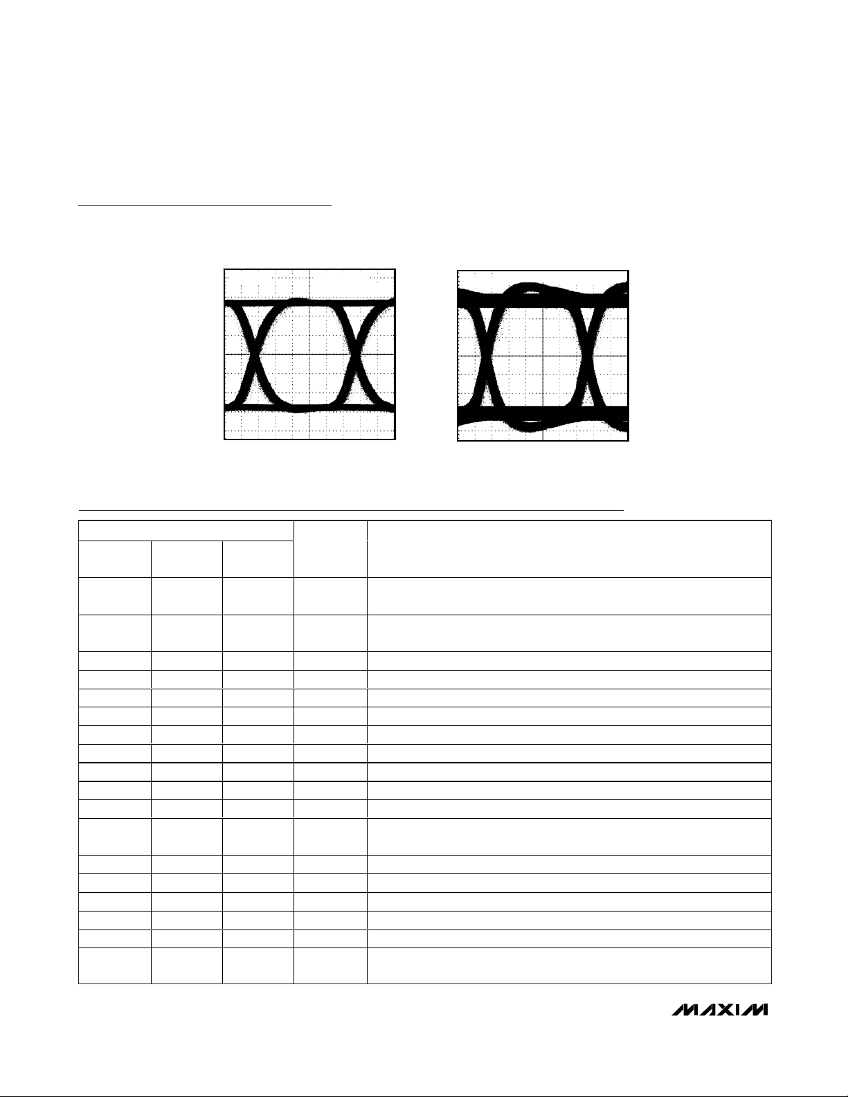
LVDS Output Preemphasis
The MAX9132/MAX9134/MAX9135 feature a preemphasis mode where extra current is added to the output
and causes the amplitude to increase by 50% at the
transition point. Preemphasis helps to get a faster transition, better eye diagram, and improved signal integrity (see the
Typical Operating Characteristics
). During
data transition, the switch injects additional current for
a short period, typically 400ps. Leave PD open or apply
a midlevel voltage (VDD/2) to enable preemphasis on
all LVDS outputs. Set PD high to set preemphasis
through the I2C or LIN interfaces. Preemphasis in this
mode is initially not on.
Power-Down
Set PD low to enable power-down mode. The registers
retain their values and the device resumes operation
from the same mode upon power-up.
MAX9132/MAX9134/MAX9135
Programmable, High-Speed, Multiple
Input/Output LVDS Crossbar Switches
______________________________________________________________________________________ 15
Figure 6. LIN Bus Wake-Up Signal
X = Don’t care.
Table 6b. Switch Routing Control Pin Setting for the MAX9135
PORT S5 S4 S3 S2 S1 S0 CONNECTION DESCRIPTION
0 0 DOUT0 connected to DIN0
0 Open DOUT0 connected to DIN1
DOUT0
DOUT1 X
DOUT2 X X
0
1 0 DOUT0 connected to DIN3
1
XXXX
1 DOUT0 connected to DIN2
XXXX
0 0 DOUT1 connected to DIN0
0 Open DOUT1 connected to DIN1
0
1 0 DOUT1 connected to DIN3
1
XX
XX
0 0 DOUT2 connected to DIN0
0 Open DOUT2 connected to DIN1
0 1 DOUT2 connected to DIN2
1 0 DOUT2 connected to DIN3
1 Open
Open
Open DOUT0 in high impedance
1 DOUT1 connected to DIN2
XX
X
DOUT1 in high impedance
DOUT2 in high impedance
S5 and S0 determine
DOUT0 connection
S4 and S1 determine
DOUT1 connection
S3 and S2 determine
DOUT2 connection
RXD
> 30µs
Page 16

MAX9132/MAX9134/MAX9135
Input/Output Termination
Terminate LVDS inputs/outputs through 100Ω differen-
tial termination, or use an equivalent Thevenin termination. Terminate both inputs/outputs and use identical
terminations on each for the lowest output-to-output
skew.
Power-Supply Bypassing
Adequate power-supply bypassing is necessary to
maximize the performance and noise immunity. Bypass
each supply to their respective grounds with highfrequency surface-mount 0.01µF ceramic capacitors as
close as possible to the device. Use multiple bypass
vias for connection to minimize inductance.
Board Layout
Separate the I2C/LIN signals and LVDS signals to prevent crosstalk. When possible, use a four-layer PCB
with separate layers for power, ground, LVDS, and digital signals. Layout PCB traces for 100Ω differential
characteristic impedance. The trace dimensions
depend on the type of trace used (microstrip or
stripline).
Route the PCB traces for an LVDS channel (there are
two conductors per LVDS channel) in parallel to maintain the differential characteristic impedance. Place the
100Ω (typ) termination resistor at both ends of the
LVDS driver and receiver. Avoid vias. If vias must be
used, use only one pair per LVDS channel and place
the via for each line at the same point along the length
of the PCB traces. This way, any reflections occur at
the same time. Do not make vias into test points for
automated test equipment. Make the PCB traces that
make up a differential pair the same length to avoid
skew within the differential pair.
Cables and Connectors
Interconnect for LVDS typically has a differential
impedance of 100Ω. Use cables and connectors that
have matched differential impedance to minimize
impedance discontinuities. Twisted-pair and shielded
twisted-pair cables offer superior signal quality compared to ribbon cable and tend to generate less EMI
due to magnetic-field-canceling effects. Balanced
cables pick up noise as common mode that is rejected
by the LVDS receiver. Add a 0.1µF capacitor in series
with each output for AC-coupling.
Choosing Pullup Resistors
I2C requires pullup resistors to provide a logic-high
level to data and clock lines. There are tradeoffs
between power dissipation and speed, and a compromise must be made in choosing pullup resistor values.
Every device connected to the bus introduces some
capacitance even when the device is not in operation.
I2C specifies 300ns rise times to go from low to high
(30% to 70%) for fast mode, which is defined for a data
rate up to 400kbps (see the
I2C Interface
section for
details). To meet the rise time requirement, choose the
pullup resistors so that the rise time tR= 0.85R
PULLUP
x
C
BUS
< 300ns. If the transition time becomes too slow,
the setup and hold times may not be met and waveforms are not recognized.
Programmable, High-Speed, Multiple
Input/Output LVDS Crossbar Switches
16 ______________________________________________________________________________________
Figure 7. Topologies for Port Expansion
DIN1 DIN2 DIN3
DIN1 DIN2 DIN3
MAX9134
DOUT1 DOUT2 DOUT3 DOUT4
3 x 8 SWITCH 6 x 4 SWITCH
DIN1 DIN2 DIN3
MAX9134
DOUT1 DOUT2 DOUT3 DOUT4
DOUT1 DOUT2 DOUT3 DOUT4
MAX9134
DIN1 DIN2 DIN3
MAX9134
DOUT1 DOUT2 DOUT3 DOUT4
Page 17

Exposed Pad
The TQFP and TSSOP packages used for the
MAX9132/MAX9134/MAX9135 have exposed pads on
the bottom. The exposed pad is internally connected to
ground. Connect the exposed pad to ground using a
landing pad large enough to accommodate the entire
exposed pad. Add vias from the exposed pad’s land
area to a copper polygon on the other side of the PCB
to provide lower thermal impedance from the device to
the ambient air.
ESD Protection
The MAX9132/MAX9134/MAX9135 ESD tolerance is
rated for IEC 61000-4-2, Human Body Model, and ISO
10605 standards. IEC 61000-4-2 and ISO 10605 specify ESD tolerance for electronic systems. The IEC
61000-4-2 discharge components are CS= 150pF and
R
D
= 330Ω (Figure 8). For IEC 61000-4-2, the LVDS
outputs are rated for ±10kV Contact Discharge and
±15kV Air-Gap Discharge. The Human Body Model
discharge components are C
S
= 100pF and RD=
1.5kΩ (Figure 9). For the Human Body Model, all pins
are rated for ±2kV Contact Discharge. The ISO 10605
discharge components are CS= 330pF and RD= 2kΩ
(Figure 10). For ISO 10605, the LVDS outputs are rated
for ±10kV Contact and ±25kV Air-Gap Discharge.
MAX9132/MAX9134/MAX9135
Programmable, High-Speed, Multiple
Input/Output LVDS Crossbar Switches
______________________________________________________________________________________ 17
Figure 8. IEC 61000-4-2 Contact Discharge ESD Test Circuit
STORAGE
CAPACITOR
HIGH-
VOLTAGE
DC
SOURCE
DEVICE
UNDER
TEST
CHARGE-CURRENT-
LIMIT RESISTOR
DISCHARGE
RESISTANCE
1MΩ
R
D
1.5kΩ
C
S
100pF
Figure 9. Human Body ESD Test Circuit
STORAGE
CAPACITOR
HIGH-
VOLTAGE
DC
SOURCE
DEVICE
UNDER
TEST
CHARGE-CURRENT-
LIMIT RESISTOR
DISCHARGE
RESISTANCE
R
D
2kΩ
C
S
330pF
Figure 10. ISO 10605 Contact Discharge ESD Test Circuit
R
D
330Ω
HIGH-
VOLTAGE
DC
SOURCE
CHARGE-CURRENT-
LIMIT RESISTOR
150pF
C
S
DISCHARGE
RESISTANCE
STORAGE
CAPACITOR
DEVICE
UNDER
TEST
Page 18

MAX9132/MAX9134/MAX9135
Programmable, High-Speed, Multiple
Input/Output LVDS Crossbar Switches
18 ______________________________________________________________________________________
Typical Application Circuit
LVDS INPUTS
0.1µF
V
DD
100Ω × 3
DIN0+ DIN0- DIN1+ DIN1- DIN2+ DIN2-
DVDD
AVDD
AGND
LVDSVDD
LVDSGND
DOUT0+ DOUT0- DOUT1+ DOUT1- DOUT2+ DOUT2- DOUT3+ DOUT3-
100Ω × 4
0.1µF
LVDS OUTPUTS
MAX9134
CONNECT S[5:0] ACCORDING
TO DESIRED INITIAL ROUTING
S0 S1 S2 S3 S4 S5
SCL/RXD
SDA/TXD
AS0
AS1/NSLP
V
DD
R
PURPU
TO I2C
MASTER
Page 19

MAX9132/MAX9134/MAX9135
Programmable, High-Speed, Multiple
Input/Output LVDS Crossbar Switches
Maxim cannot assume responsibility for use of any circuitry other than circuitry entirely embodied in a Maxim product. No circuit patent licenses are
implied. Maxim reserves the right to change the circuitry and specifications without notice at any time.
Maxim Integrated Products, 120 San Gabriel Drive, Sunnyvale, CA 94086 408-737-7600 ____________________
19
© 2008 Maxim Integrated Products is a registered trademark of Maxim Integrated Products, Inc.
Chip Information
PROCESS: CMOS
Pin Configurations (continued)
MAX9134
TQFP-EP*
TOP VIEW
29
30
28
27
12
11
13
14
1
+
24567
2324 22 20 19 18
S5
S4
S3
S2
S1
S0
3
21
31
10
32
9
26
15
25
16
8
17
SCL/RXD
LVDSVDD
DOUT0+
DIN0-
DIN0+
DVDD
PD
DOUT0-
DOUT1+
DOUT1-
DOUT2+
DOUT2-
DOUT3+
DOUT3-
LVDSGND
LVDSVDD
LVDSGND
DIN2-
DIN2+
DIN1-
DIN1+
AS1/NSLP
AS0
*EXPOSED PAD. CONNECT EP TO GND.
AVDD
AGND
SDA/TXD
Package Information
For the latest package outline information and land patterns, go
to www.maxim-ic.com/packages
.
PACKAGE TYPE PACKAGE CODE DOCUMENT NO.
20 TSSOP-EP U20E+1
21-0108
32 TQFP-EP H32E+6
21-0079
DOUT0+
LVDSGND
DOUT0-
DOUT1+
DOUT1-
LVDSGND
DOUT2+
DIN3+
DOUT2-
17
8
DIN3-
TOP VIEW
2324 22 20 19 18
DVDD
DGND
25
26
27
28
S5
29
S4
30
PD
31
32
+
24567
1
DIN0-
DIN0+
LVDSVDD
SDA/TXD
SCL/RXD
*EXPOSED PAD. CONNECT EP TO GND.
21
MAX9135
3
DIN1-
DIN1+
TQFP-EP*
DIN2+
DIN2-
16
15
14
13
12
11
10
9
LVDSVDD
AS1/NSLP
AS0
S3
S2
S1
S0
AVDD
 Loading...