

Page 1
MAX9107/MAX9108/MAX9109
25ns, Dual/Quad/Single, Low-Power,
TTL Comparators
________________________________________________________________ Maxim Integrated Products 1
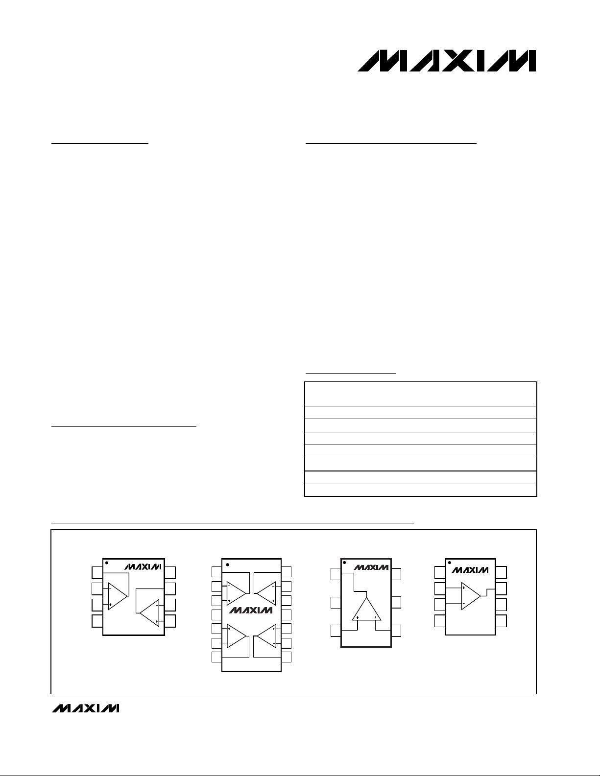
Pin Configurations
19-2045; Rev. 0; 5/01
General Description
The MAX9107/MAX9108/MAX9109 dual/quad/single,
high-speed, low-power voltage comparators are
designed for use in systems powered from a single
+5V supply. Their 25ns propagation delay (with 10mV
input overdrive) is achieved with a power consumption
of only 1.75mW per comparator. The wide input common-mode range extends from 200mV below ground
to within 1.5V of the positive supply rail.
The MAX9107/MAX9108/MAX9109 outputs are TTLcompatible, requiring no external pullup circuitry.
These easy-to-use comparators incorporate internal
hysteresis to ensure clean output switching even when
the devices are driven by a slow-moving input signal.
The MAX9107/MAX9108/MAX9109 are higher-speed,
lower-power, lower-cost upgrades to industry-standard
comparators MAX907/MAX908/MAX909. The MAX9109
features an output latch but does not have complementary outputs.
The dual MAX9107 is available in both 8-pin SO and
SOT23 packages. The quad MAX9108 is available in
14-pin TSSOP and SO packages while the single
MAX9109 is available in an ultra-small 6-pin SC70
package, a space-saving 6-pin SOT23 package and
an 8-pin SO package.
Applications
Features
♦ 25ns Propagation Delay
♦ 350µA (1.75mW) Supply Current Per Comparator
♦ Single 4.5V to 5.5V Supply Operation
♦ Wide Input Range Includes Ground
♦ Low 500µV Offset Voltage
♦ Internal Hysteresis Provides Clean Switching
(2mV)
♦ TTL-Compatible Outputs
♦ Internal Latch (MAX9109 only)
♦ No Phase Reversal for Overdriven Inputs
♦ Space-Saving Packages:
6-Pin SC70 (MAX9109)
8-Pin SOT23 (MAX9107)
14-Pin TSSOP (MAX9108)
Ordering Information
Battery-Powered Systems
A/D Converters
Line Receivers
Threshold Detectors/
Discriminators
Sampling Circuits
Zero-Crossing Detectors
For pricing, delivery, and ordering information, please contact Maxim/Dallas Direct! at
1-888-629-4642, or visit Maxim’s website at www.maxim-ic.com.
PART TEMP. RANGE
MAX9107EKA-T -40°C to +85°C 8 SOT23-8 AAIB
MAX9107ESA -40°C to +85°C 8 SO —
MAX9108EUD -40°C to +85°C 14 TSSOP —
MAX9108ESD -40°C to +85°C 14 SO —
MAX9109EXT-T -40°C to +85°C 6 SC70-6 AAU
MAX9109EUT-T -40°C to +85°C 6 SOT23-6 AARU
MAX9109ESA -40°C to +85°C 8 SO —
PINPACKAGE
TOP
MARK
TOP VIEW
OUTA
INA-
INA+
GND
OUTA
INA-
INA+
INB+
INB-
CC
1
2
3
4
5
6
7
A
MAX9108
B
TSSOP/SO
1
2
3
4
MAX9107
SOT23/SO
V
CC
OUTB
7
6
INB-
INB+
5
14
OUTD
OUT
13
IND-
D
12
IND+
GND
11
GNDV
INC+
10
C
9
INC-
OUTCOUTB
8
MAX9109
16V
2
34
SC70/SOT23
CC
5 LE
IN-IN+
8
V
IN+
N.C.
1
CC
IN-
MAX9109
2
3
4
SO
8
N.C.
OUT
7
6
GND
LE
5
Page 2
MAX9107/MAX9108/MAX9109
25ns, Dual/Quad/Single, Low-Power,
TTL Comparators
2 _______________________________________________________________________________________
Power-Supply Ranges
Supply Voltage (V
CC
to GND)..............................................6V
Differential Input Voltage........................-0.3V to (V
CC
+ 0.3V)
Common-Mode Input Voltage to GND ...-0.3V to (V
CC
+ 0.3V)
Latch-Enable Input Voltage
(MAX9109 only)...................................-0.3V to (V
CC
+ 0.3V)
Output Short-Circuit Duration to V
CC
or GND ........................10s
Continuous Power Dissipation (T
A
= +70°C)
6-Pin SC70 (derate 3.1mW/°C above +70°C)..............245mW
6-Pin SOT23 (derate 8.7mW/°C above +70°C)............696mW
8-Pin SOT23 (derate 9.1mW/°C above +70°C)............727mW
8-Pin SO (derate 5.9mW/°C above +70°C)..................470mW
14-Pin TSSOP (derate 9.1mW/°C above +70°C) .........727mW
14-Pin SO (derate 8.33mW/°C above +70°C)..............666mW
Operating Temperature Range ...........................-40°C to +85°C
Storage Temperature Range .............................-65°C to +150°C
Lead Temperature (soldering, 10s) .................................+300°C
ELECTRICAL CHARACTERISTICS
(VCC= +5V, VCM= 0, VLE= 0 (MAX9109 only), TA= T
MIN
to T
MAX
, unless otherwise noted. Typical values are at TA= +25°C.) (Note 1)
Stresses beyond those listed under “Absolute Maximum Ratings" may cause permanent damage to the device. These are stress ratings only, and functional
operation of the device at these or any other conditions beyond those indicated in the operational sections of the specifications is not implied. Exposure to
absolute maximum rating conditions for extended periods may affect device reliability.
ABSOLUTE MAXIMUM RATINGS
PARAMETER
Operating Voltage Range
Input Bias Current
Input Offset Current
Common-Mode Rejection Ratio
Power-Supply Rejection Ratio
Output High Voltage
Output Low Voltage
Output Rise Time
Output Fall Time
t
f
t
r
V
OL
V
OH
PSRR
CMRR
I
OS
I
B
V
CC
SYMBOL
V
OUT
= 2.4V to 0.4V, CL= 10pF
V
OUT
= 0.4V to 2.4V, CL= 10pF
I
SINK
= 8mA
I
SINK
= 3.2mA
I
SOURCE
= 100µA
4.5V ≤ V
CC
≤ 5.5V
VCC= 5.5V (Note 5)
TA= +25°C
Guaranteed by PSRR
CONDITIONS MIN TYP MAX
4.5 5.5
0.5 1.6
125 350
25 80
50 1000
50 1000
3.0 3.5
0.35 0.6
0.4
12
6 ns
ns
V
V
µV/V
µV/V
nA
nA
V
UNITS
Input Hysteresis
V
HYST
(Note 3) 2 mV
Input Voltage Range
V
CMR
(Note 4) -0.2 VCC- 1.5 V
mASupply Current Per Comparator VCC= +5.5V, all outputs low
I
CC
0.35 0.7
Input Offset Voltage
V
OS
TA= T
MIN
to T
MAX
4.0
mV
(Note 2)
Page 3
MAX9107/MAX9108/MAX9109
25ns, Dual/Quad/Single, Low-Power,
TTL Comparators
_______________________________________________________________________________________ 3
ELECTRICAL CHARACTERISTICS (continued)
(VCC= +5V, VCM= 0, VLE= 0 (MAX9109 only), TA= T
MIN
to T
MAX
, unless otherwise noted. Typical values are at TA= +25°C.) (Note 1)
Latch Hold Time
Latch Setup Time
Latch Input Current
Latch Input Voltage Low
Latch Input Voltage High
Propagation Delay Skew
Differential Propagation Delay
Propagation Delay
PARAMETER SYMBOL
t
PD+,tPD-
∆t
PD
tPDskew
V
IH
V
IL
IIH, I
IL
t
s
t
h
(Note 8)
(Note 8)
(Note 8)
(Note 8)
(Note 8)
VIN= 100mV, VOD= 10mV
(Note 7)
VIN= 100mV, VOD= 10mV
(Note 6)
VIN= 100mV, VOD= 10mV
CONDITIONS MIN TYP MAX
25
1
5
2.0
0.8
0.4 1
2
2 ns
ns
µA
V
V
ns
ns
ns
UNITS
Note 1: Devices are 100% production tested at TA= +25°C. All temperature limits are guaranteed by design.
Note 2: Input Offset Voltage is defined as the center of the input-referred hysteresis zone. Specified for V
CM
= 0. See Figure 1.
Note 3: Trip Point is defined as the input voltage required to make the comparator output change state. The difference
between upper (V
TRIP
+) and lower (V
TRIP
-) trip points is equal to the width of the input-referred hysteresis zone (V
HYST
).
Specified for an input common-mode voltage (V
CM
) of 0. See Figure 1.
Note 4: Inferred from the CMRR test. Note that a correct logic result is obtained at the output, provided that at least one input is
within the V
CMR
limits. Note also that either or both inputs can be driven to the upper or lower absolute maximum limit with-
out damage to the part.
Note 5: Tested over the full-input voltage range (V
CMR
).
Note 6: Differential Propagation Delay is specified as the difference between any two channels in the MAX9107/MAX9108 (both
outputs making either a low-to-high or a high-to-low transition).
Note 7: Propagation Delay Skew is specified as the difference between any single channel’s output low-to-high transition (t
PD
+)
and high-to-low transition (t
PD
-).
Note 8: Latch specifications apply to MAX9109 only. See Figure 2.
Page 4
MAX9107/MAX9108/MAX9109
25ns, Dual/Quad/Single, Low-Power,
TTL Comparators
4 ________________________________________________________________________________________________
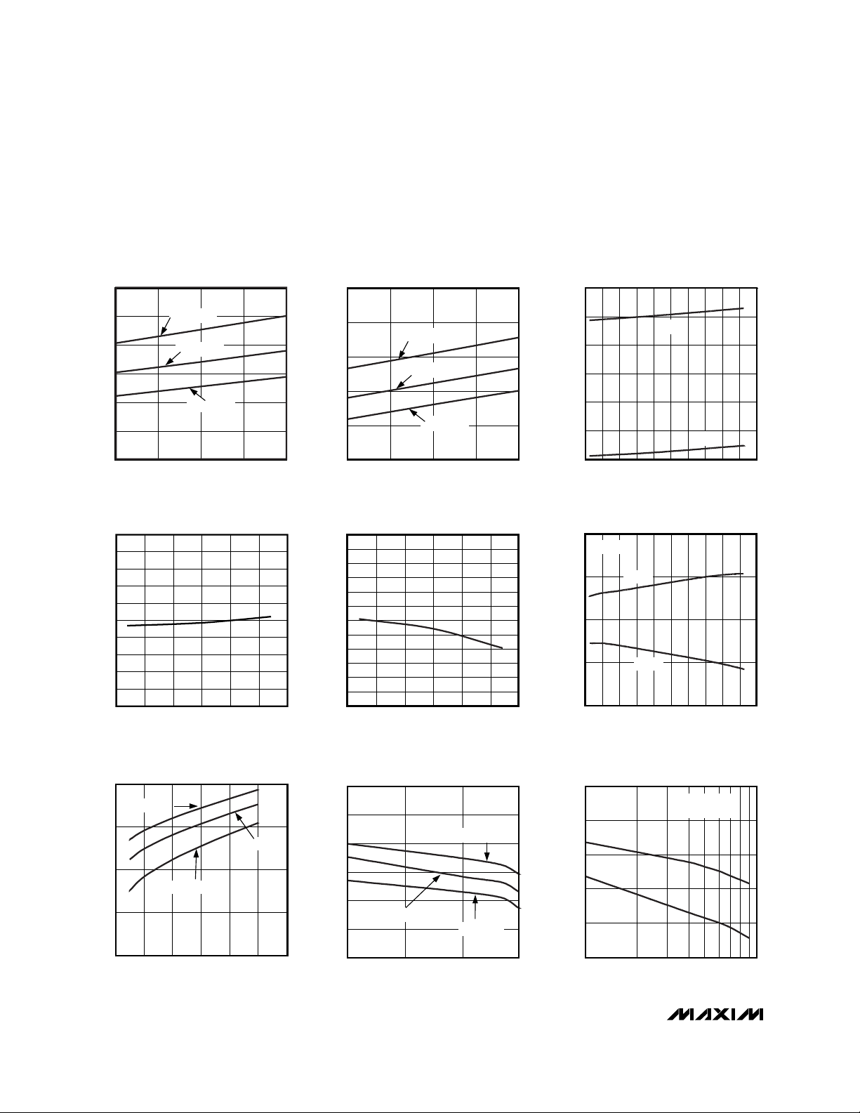
__________________________________________Typical Operating Characteristics
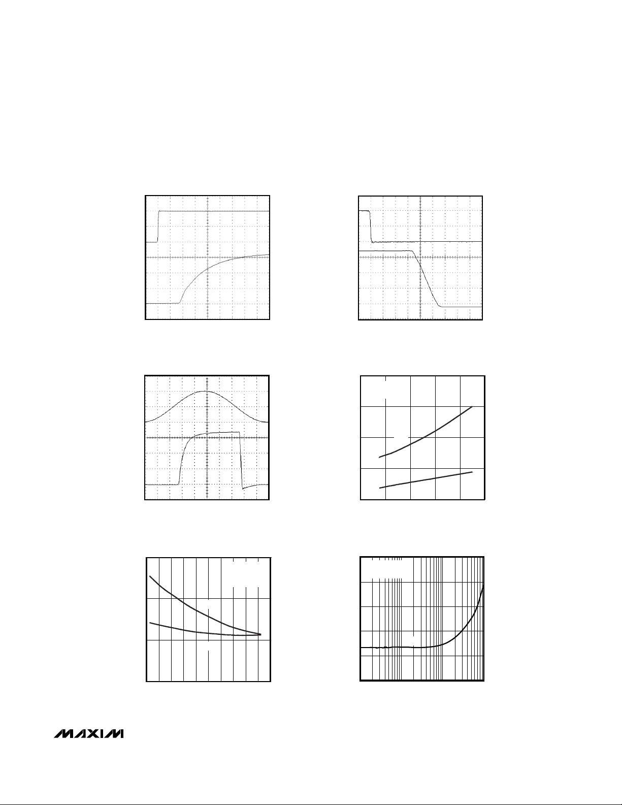
(VCC= 5V, VCM= 0, CL= 15pF, TA= +25°C, unless otherwise noted.)
0.6
SUPPLY CURRENT
vs. SUPPLY VOLTAGE
(OUTPUTS AT V
OL
SUPPLY CURRENT
)
0.5
(OUTPUTS AT V
)
OH
5
vs. SUPPLY VOLTAGE
INPUT VOLTAGE RANGE
vs. TEMPERATURE
0.5
0.4
0.3
0.2
SUPPLY CURRENT (mA)
0.1
0
4.0 5.04.5 5.5 6.0
0.5
0.4
0.3
0.2
0.1
0
-0.1
-0.2
INPUT OFFSET VOLTAGE (mV)
-0.3
-0.4
-0.5
-50 0-25 25 50 75 100
TA = +125°C
TA = +25°C
TA = -55°C
SUPPLY VOLTAGE (V)
INPUT OFFSET VOLTAGE
vs. TEMPERATURE
TEMPERATURE (°C)
0.4
MAX9107/08/09 toc01
0.3
0.2
SUPPLY CURRENT (mA)
0.1
0
200
150
100
50
MAX9107/08/09 toc04
0
-50
-100
-150
-200
INPUT CURRENT (nA)
-250
-300
-350
-400
TA = +125°C
TA = +25°C
TA = -55°C
4.0 5.04.5 5.5 6.0
SUPPLY VOLTAGE (V)
INPUT BIAS CURRENT
vs. TEMPERATURE
-50 0 25-25 50 75 100
TEMPERATURE (°C)
4
MAX9107/08/09 toc02
MAX9107/08/09 toc05
3
2
1
INPUT VOLTAGE RANGE (V)
0
-1
-60 200-40 -20 40 60 80 100 120 140
2
1
(mV)
0
OS
V
-1
-2
-60 -20 0 20 40-40 60 80 100 120 140
vs. TEMPERATURE
VCM = 0
V
TRIP+
V
CMR+
V
TEMPERATURE (°C)
TRIP POINT
V
TRIP-
TEMPERATURE (°C)
MAX9107/08/09 toc03
CMR-
MAX9107/08/09 toc06
OUTPUT LOW VOLTAGE
vs. SINK CURRENT
0.5
TA = -55°C
0.4
TA = +25°C
(V)
0.3
OL
V
0.2
0.1
0624 81012
TA = +125°C
I
SINK
(mA)
5.0
4.5
MAX9107/08/09 toc07
4.0
(V)
3.5
OH
V
3.0
2.5
2.0
OUTPUT HIGH VOLTAGE
vs. SOURCE CURRENT
TA = +125°C
TA = +25°C
TA = -55°C
1 100 1000
10
I
SOURCE
(µA)
35
30
MAX9107/08/09 toc08
25
20
PROPAGATION DELAY (ns)
15
10
PROPAGATION DELAY
vs. INPUT OVERDRIVE
t
t
PD-
10 100
INPUT OVERDRIVE (mV)
PD+
RS = 10
C
LOAD
Ω
= 15pF
MAX9107/08/09 toc09
Page 5
MAX9107/MAX9108/MAX9109
25ns, Dual/Quad/Single, Low-Power,
TTL Comparators
_________________________________________________________________________________________________ 5
____________________________Typical Operating Characteristics (continued)
(VCC= 5V, VCM= 0, CL= 15pF, TA= +25°C, unless otherwise noted.)
PROPAGATION DELAY (t
PD+
)
PROPAGATION DELAY (t
PD-
)
INPUT
50mV/div
OVERDRIVE
10mV
OUTPUT
1V/div
INPUT
50mV/div
OUTPUT
1V/div
10ns/div
SINUSOID 2MHz RESPONSE
50ns/div
MAX9107/08/09 toc10
MAX9107/08/09 toc12
INPUT
50mV/div
OVERDRIVE
10mV
OUTPUT
1V/div
40
35
30
PROPAGATION DELAY (ns)
25
20
5ns/div
PROPAGATION DELAY
vs. CAPACITIVE LOAD
VOD = 10mV
= 10
R
Ω
S
t
PD+
t
PD-
04020 60 80 100
CAPACITIVE LOAD (pF)
MAX9107/08/09 toc11
MAX9107/08/09 toc13
PROPAGATION DELAY
vs. TEMPERATURE
40
30
20
PROPAGATION DELAY (ns)
10
-60 200-40 -20 40 60 80 100 120 140
TEMPERATURE (°C)
VOD = 10mV
= 10
R
S
C
LOAD
t
PD+
t
PD-
Ω
= 15pF
MAX9107/08/09 toc14
100
80
60
40
PROPAGATION DELAY (ns)
20
0
PROPAGATION DELAY
vs. SOURCE IMPEDANCE
VOD = 5mV
= 15pF
C
LOAD
10 10k1k100
SOURCE IMPEDANCE (Ω)
MAX9107/08/09 toc15
t
PD+
Page 6
MAX9107/MAX9108/MAX9109
25ns, Dual/Quad/Single, Low-Power,
TTL Comparators
6 _______________________________________________________________________________________
_______________Detailed Description
Timing
Noise or undesired parasitic AC feedback cause most
high-speed comparators to oscillate in the linear region
(i.e., when the voltage on one input is at or near the
voltage on the other input). The MAX9107/MAX9108/
MAX9109 eliminate this problem by incorporating an
internal hysteresis of 2mV. When the two comparator
input voltages are equal, hysteresis effectively causes
one comparator input voltage to move quickly past the
other, thus taking the input out of the region where
oscillation occurs. Standard comparators require that
hysteresis be added through the use of external resistors. The MAX9107/MAX9108/MAX9109’s fixed internal
hysteresis eliminates these resistors. To increase hysteresis and noise margin even more, add positive feedback with two resistors as a voltage divider from the
output to the noninverting input.
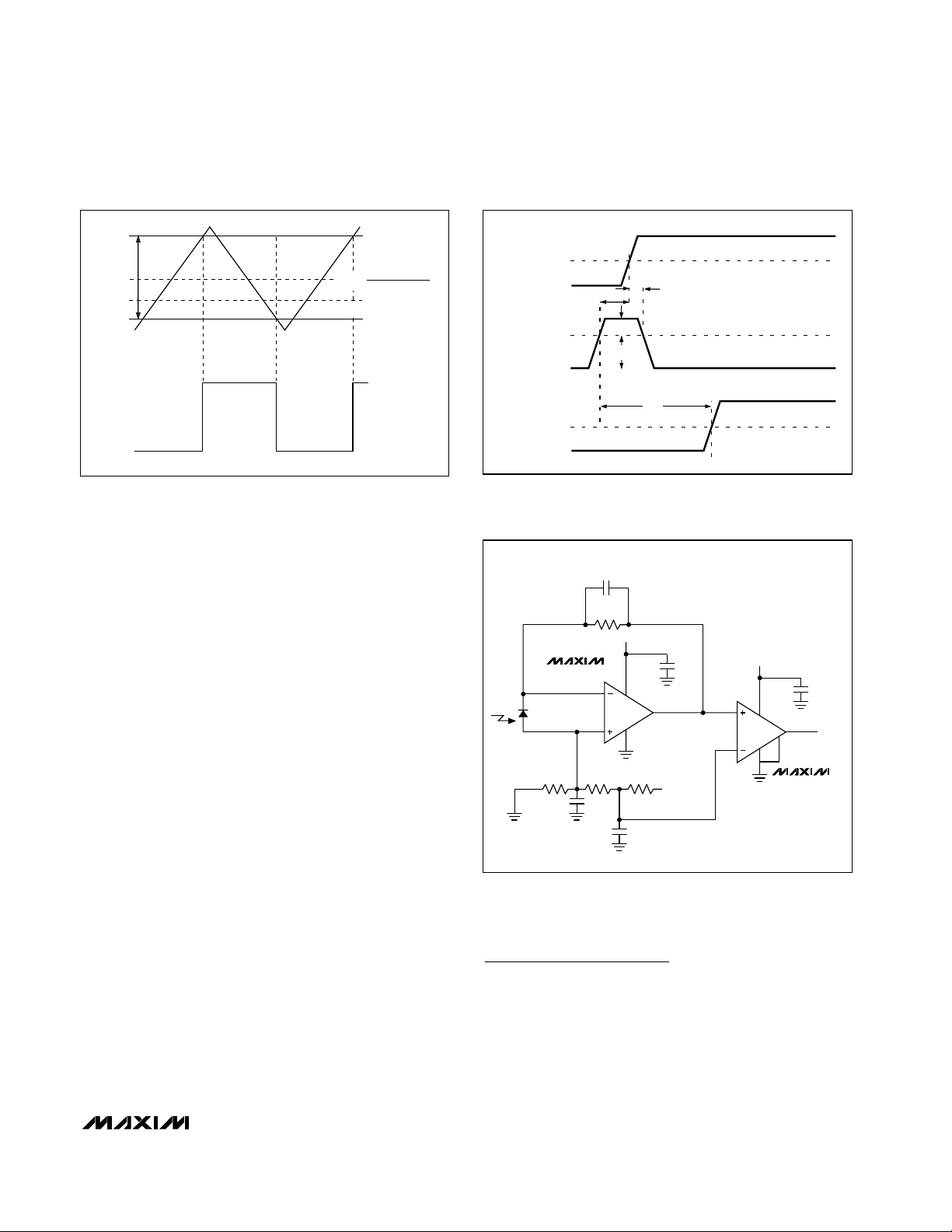
Adding hysteresis to a comparator creates two trip
points: one for the input voltage rising and one for the
input voltage falling (Figure 1). The difference between
these two input-referred trip points is the hysteresis.
The average of the trip points is the offset voltage.
Figure 1 illustrates the case where IN- is fixed and IN+
is varied. If the inputs were reversed, the figure would
look the same, except the output would be inverted.
The MAX9109 includes an internal latch, allowing the
result of a comparison to be stored. If LE is low, the
latch is transparent (i.e., the comparator operates as
though the latch is not present). The state of the comparator output is latched when LE is high (Figure 2).
Applications Information
Circuit Layout
Because of the MAX9107/MAX9108/MAX9109’s high
gain bandwidth, special precautions must be taken to
realize the full high-speed capability. A printed circuit
board with a good, low-inductance ground plane is
mandatory. Place the decoupling capacitor (a 0.1µF
ceramic capacitor is a good choice) as close to VCCas
______________________________________________________________Pin Description
MAX9107 MAX9108
11 ——OUTA Channel A Output
22 ——INA- Channel A Inverting Input
33 ——INA+ Channel A Noninverting Input
77 ——OUTB Channel B Output
66 ——INB- Channel B Inverting Input
55 ——INB+ Channel B Noninverting Input
— 8 ——OUTC Channel C Output
— 9 ——INC- Channel C Inverting Input
— 10 ——INC+ Channel C Noninverting Input
— 14 ——OUTD Channel D Output
— 13 ——IND- Channel D Inverting Input
— 12 ——IND+ Channel D Noninverting Input
—— 1 7 OUT Output
—— 3 2 IN+ Noninverting Input
—— 4 3 IN- Inverting Input
8461V
4 11 2 6 GND Ground
—— 5 5 LE Latch E nab l e. The l atch i s tr ansp ar ent w hen LE i s l ow .
—— — 4, 8 N.C. No Connection. Not internally connected.
PIN
MAX9109
SC70/SOT23 SO
NAME FUNCTION
CC
Positive Supply
Page 7
MAX9107/MAX9108/MAX9109
25ns, Dual/Quad/Single, Low-Power,
TTL Comparators
_______________________________________________________________________________________ 7
V
Figure 1. Input and Output Waveforms, Noninverting Input
Varied
possible. Pay close attention to the decoupling capacitor’s bandwidth, keeping leads short. Short lead
lengths on the inputs and outputs are also essential to
avoid unwanted parasitic feedback around the comparators. Solder the device directly to the printed circuit
board instead of using a socket.
Overdriving the Inputs
The inputs to the MAX9107/MAX9108/MAX9109 may be
driven to the voltage limits given in the Absolute
Maximum Ratings. If the inputs are overdriven, there is
no output phase reversal.
Battery-Operated Infrared Data Link
In Figure 3, the circuit allows reception of infrared data.
The MAX4400 converts the photodiode current to a
voltage, and the MAX9109 determines whether the
amplifier output is high enough to be called a “1.” The
current consumption of this circuit is minimal: the
MAX4400 and MAX9109 require typically 410µA and
350µA, respectively.
Figure 2. MAX9109 Timing Diagram
Figure 3. Battery-Operated Infrared Data Link Consumes Only
760µA
Chip Information
MAX9107 TRANSISTOR COUNT: 262
MAX9108 TRANSISTOR COUNT: 536
MAX9109 TRANSISTOR COUNT: 140
PROCESS: Bipolar
TRIP+
V
HYST
V
TRIP-
COMPARATOR
OUTPUT
3V
V
IN+
V
+ V
TRIP+
V
=
OS
V
= 0
IN-
TRIP-
2
V
OH
V
OL
LE
DIFFERENTIAL
INPUT
VOLTAGE
OUTPUT
1.4V
V
V
1.4V
V
0
OS
OH
OL
COMPARE
LATCH
t
h
t
s
V
OD
V
IN
tPD+
10pF
1M
Ω
MAX4400
SIEMENS BP-104
PHOTODIODE
100k
Ω
1000pF
1000pF
47k
+5V
3
1
100k
Ω
0.1µF
5
4
2
Ω
+5V
+5V
3
4
2
0.1µF
6
1
DATA
5
MAX9109
Page 8

MAX9107/MAX9108/MAX9109
25ns, Dual/Quad/Single, Low-Power,
TTL Comparators
8 _______________________________________________________________________________________
Package Information
SOT23, 8L.EPS
TSSOP.EPS
Page 9

MAX9107/MAX9108/MAX9109
25ns, Dual/Quad/Single, Low-Power,
TTL Comparators
_______________________________________________________________________________________ 9
Package Information (continued)
SC70, 6L.EPS
6LSOT.EPS
Page 10

MAX9107/MAX9108/MAX9109
25ns, Dual/Quad/Single, Low-Power,
TTL Comparators
Maxim cannot assume responsibility for use of any circuitry other than circuitry entirely embodied in a Maxim product. No circuit patent licenses are
implied. Maxim reserves the right to change the circuitry and specifications without notice at any time.
10 ____________________Maxim Integrated Products, 120 San Gabriel Drive, Sunnyvale, CA 94086 408-737-7600
© 2001 Maxim Integrated Products Printed USA is a registered trademark of Maxim Integrated Products.
Package Information (continued)
SOICN.EPS
 Loading...