

Page 1
General Description
The MAX9100/MAX9101 micropower comparators are
optimized for single-cell systems, and are fully specified for operation from a single supply of +1.0V to
+5.5V. This ultra-low voltage operation, 5µA quiescent
current consumption, and small footprint make the
MAX9100/MAX9101 ideal for use in battery-powered
systems. A wide-input common-mode range that
includes the negative rail and Rail-to-Rail®output swing
allows almost all of the power supply to be used for signal voltage. In addition, propagation delay is less than
4µs, and rise and fall times are 100ns.
The MAX9100 features a push-pull CMOS output stage
that sinks and sources current with large internal output
drivers that allow rail-to-rail output swings with loads up
to 5mA.The MAX9101 has an open-drain output stage
that makes it suitable for mixed-voltage designs.
The MAX9100/MAX9101 are available in tiny SOT23-5
packages.
________________________Applications
Single-Cell Systems
Pagers
Closed Sensor Applications
Battery-Powered Instrumentation
Portable Electronic Equipment
Portable Communication Devices
____________________________Features
• Ultra-Low Voltage: Guaranteed Down to +1.0V
• Low Quiescent Current: 5µA
• Optimized for Single-Cell Battery-Powered
Systems
• Wide Input Common-Mode Range
• CMOS Rail-to-Rail Output Swing (MAX9100)
• Open-Drain Output (MAX9101)
• 4µs Propagation Delay
• High Output Drive Capability: 5mA Sink and
Source (MAX9100)
• No Output Phase Reversal for Overdriven Inputs
• Available in Tiny SOT23-5 Package
MAX9100/MAX9101
+1.0V Micropower SOT23 Comparators
GND
IN-
IN+
1
5
V
CC
OUT
MAX9100
MAX9101
SOT23
TOP VIEW
2
3
4
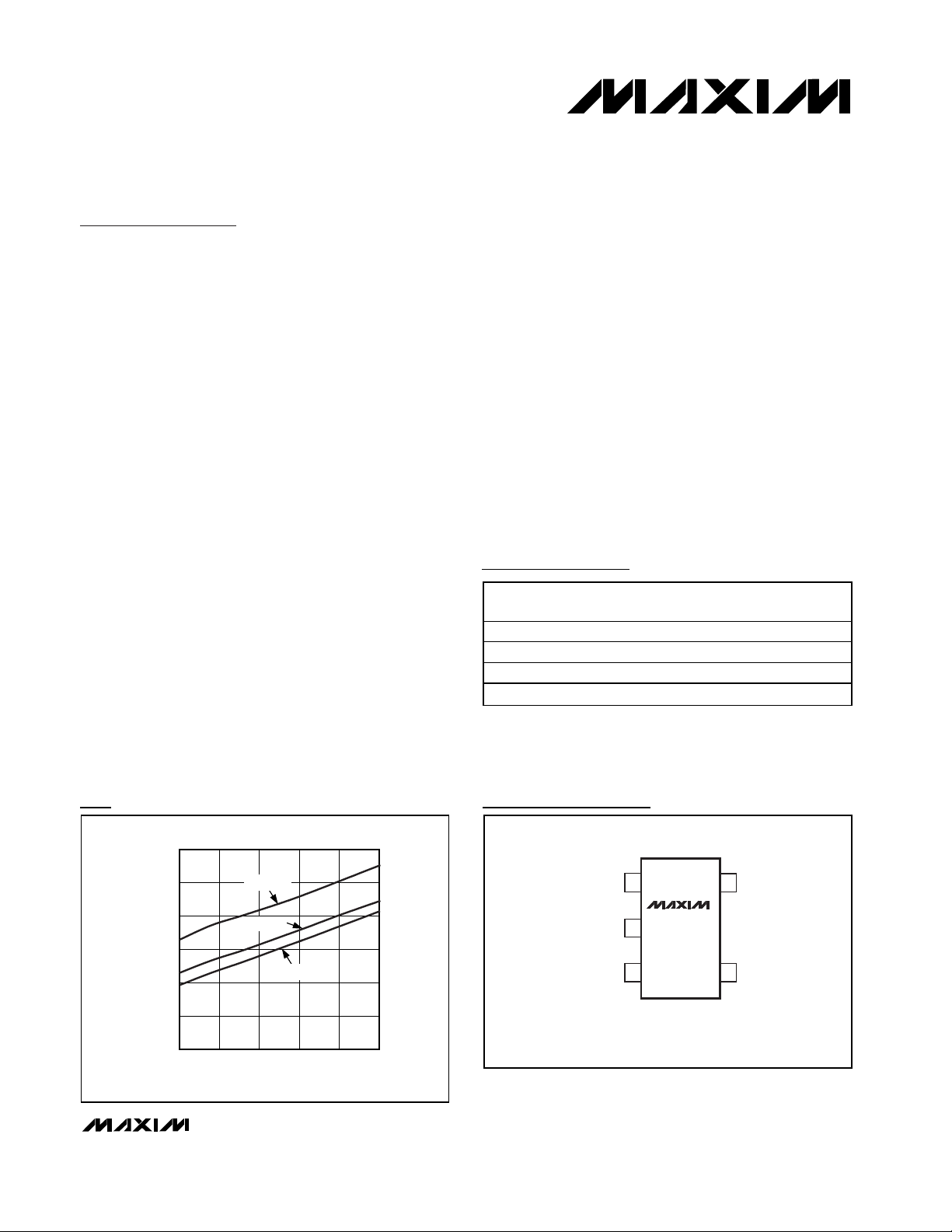
Typical Operating Characteristic
2
4
3
6
5
7
8
-40 10-15 35 60 85
SUPPLY CURRENT vs. TEMPERATURE
MAX9100 toc01
TEMPERATURE (°C)
I
CC
(µA)
VCC = +5V
VCC = +2V
VCC = +1V
19-1808; Rev 0; 10/00
Ordering Information
Pin Configurations
Pin Configurations continued at end of data sheet.
________________________________________________________________ Maxim Integrated Products 1
Rail-to-Rail is a registered trademark of Nippon Motorola, Ltd.
For price, delivery, and to place orders, please contact Maxim Distribution at 1-888-629-4642,
or visit Maxim’s website at www.maxim-ic.com.
PART TEMP. RANGE
MAX9100EUK-T -40°C to +85°C 5 SOT23-5 ADOR
MAX9100ESA -40°C to +85°C 8 SO —
MAX9101EUK-T -40°C to +85°C 5 SOT23-5 ADOS
MAX9101ESA -40°C to +85°C 8 SO —
PINPACKAGE
TOP
MARK
Page 2
MAX9100/MAX9101
+1.0V Micropower SOT23 Comparators
2 _______________________________________________________________________________________
ABSOLUTE MAXIMUM RATINGS
ELECTRICAL CHARACTERISTICS
(VCC= +1.2V to +5.5V, VCM= 0, and TA= T
MIN
to T
MAX
, unless otherwise noted. Typical values are at TA= +25°C.) (Note 1)
Stresses beyond those listed under “Absolute Maximum Ratings” may cause permanent damage to the device. These are stress ratings only, and functional
operation of the device at these or any other conditions beyond those indicated in the operational sections of the specifications is not implied. Exposure to
absolute maximum rating conditions for extended periods may affect device reliability.
Supply Voltage (VCCto GND) ................................. -0.3V to +6V
IN+ or IN- to GND...................................... -0.3V to (V
CC
+ 0.3V)
Output Voltages to GND
MAX9100.............................................. -0.3V to (V
CC
+ 0.3V)
MAX9101 ............................................................ -0.3V to +6V
Output Short-Circuit Duration (to V
CC
or GND)......... Continuous
Continuous Power Dissipation (T
A
= +70°C)
5-Pin Plastic SOT23
(derate 7.3mW/°C above +70°C)............................... 571mW
8-Pin Plastic SO
(derate 5.88mW/°C above +70°C)............................. 471mW
Operating Temperature Range .......................... -40°C to +85°C
Junction Temperature..................................................... +150°C
Storage Temperature Range ............................ -65°C to +150°C
Lead Temperature (soldering, 10s) .................................+300°C
PARAMETER SYMBOL CONDITIONS MIN TYP MAX UNITS
Supply Voltage Range V
Supply Current I
Input Offset Voltage V
Input Hysteresis V
Input Offset Current I
Input Bias Current I
Input Resistance R
Input Common-Mode Voltage
Range (Note 2)
Common-Mode
Rejection Ratio (Note 3)
Power-Supply
Rejection Ratio
Output Voltage Low V
HYST
V
CMRR
PSRR
C C
CC
CC
OS
OS
B
IN
CM
- V
OL
Inferred from the PSRR tests 1.0 5.5 V
VCC = +1V, TA = +25°C 5.0 8.0
VCC = +5V, TA = T
TA = +25°C ±3 ±10
TA = T
MIN
to T
MAX
VCC = +5.5V, TA = +25°C ±0.1 ±5
VCC = +5.5V, TA = T
VCC = +5.5V, TA = +25°C ±5 ±15
VCC = +5.5V, TA = T
Differential mode 200
Common mode 65
Inferred from CMRR test 0 V
TA = +25°C5468
= T
MIN
to T
MAX
T
A
1.0V ≤ VCC ≤ 1.5V, TA = +25°C5466
1.5V ≤ V
VCC = +5.0V, I
VCC = +1.2V, I
OH
VCC = +1.0V, I
VCC = +5.0V, I
VCC = +1.2V, I
VCC = +1.0V, I
≤ 5.5V, TA = -40°C to +85°C5668
CC
SOURCE
SOURCE
SOURCE
SINK
SINK
SINK
MIN
to T
MAX
6.0 13.0
±20
±2mV
MIN
MIN
to T
to T
MAX
MAX
±10
±30
- 0.2 V
C C
46
= 5mA 90 180
= 0.5mA 60 120Output Voltage High (MAX9100) V
= 0.1mA, TA =
25 75
= 5mA 100 180
= 0.5mA 45 120
= 0.5mA, TA = +25°C1575
µA
mV
nA
nA
MΩ
dB
dB
mV
mV
Page 3
MAX9100/MAX9101
+1.0V Micropower SOT23 Comparators
_______________________________________________________________________________________ 3
ELECTRICAL CHARACTERISTICS (continued)
(VCC= +1.2V to +5.5V, VCM= 0, and TA= T
MIN
to T
MAX
, unless otherwise noted. Typical values are at TA= +25°C.) (Note 1)
Note 1: All specifications are 100% production tested at TA= +25°C. All temperature limits are guaranteed by design.
Note 2: Operation with V
CM
up to VCCis possible with reduced accuracy. See Input Stage Circuitry and Rail-to-Rail Operation in
the Applications section for more information.
Note 3: Tested over the specified Input Common-Mode Voltage Range and with V
CC
= +5.5V.
Note 4: Specified with C
L
= 15pF for MAX9100/MAX9101, and with R
PULLUP
= 5kΩ for MAX9101.
Note 5: Input overdrive is defined above and beyond the offset voltage and hysteresis of the comparator input.
Output Short-Circuit Current I
Output Open-Drain Leakage
Current (MAX9101)
Power-Up Time t
Input Capacitance C
Output Rise Time (MAX9100) t
Output Fall Time (Note 4) t
Propagation Delay (Note 5)
PARAMETER SYMBOL CONDITIONS MIN TYP MAX UNITS
I
LKG
rise
t
pd+
t
pd-
t
pd+
t
pd-
SC
PU
fall
IN
Sourcing
(MAX9100)
Sinking
VCC = +5.5V 0.02 0.2 µA
CL = 15pF 100 ns
CL = 15pF 100 ns
V
OVERDRIVE
V
OVERDRIVE
V
OVERDRIVE
V
OVERDRIVE
VCC = +5.0V 25
= +1.2V 3
V
CC
VCC = +5.0V 28
= +1.2V 3
V
CC
250 ns
3pF
= 50mV, VCC = +5.0V 3.4
= 50mV, VCC = +5.0V 4.5
= 50mV, VCC = +1.0V 3.3
= 50mV, VCC = +1.0V 3.7
mA
µs
Page 4

Typical Operating Characteristics
(VCC= +5V, VCM= 0, TA= +25°C, unless otherwise noted.)
MAX9100/MAX9101
+1.0V Micropower SOT23 Comparators
4 _______________________________________________________________________________________
SUPPLY CURRENT vs. TEMPERATURE
8
600
OUTPUT VOLTAGE LOW
vs. SINK CURRENT
600
OUTPUT VOLTAGE HIGH
vs. SOURCE CURRENT
7
6
(µA)
5
CC
I
4
3
2
-40 10-15 356085
900
800
700
600
500
(nA)
400
BIAS
I
300
200
100
0
-100
021 345
VCC = +5V
VCC = +2V
VCC = +1V
TEMPERATURE (°C)
INPUT BIAS CURRENT vs. V
I
= I
BIAS(-)
BIAS(+)
VCM(V)
MAX9100 toc01
(mV)
V
CM
MAX9100 toc04
500
400
VCC = +1V
300
VCC = +1.2V
OL
200
100
0
01051520
VCC = +2V
I
(mA)
LOAD
VCC = +5V
MAX1900 toc02
SUPPLY CURRENT vs. SUPPLY VOLTAGE
7.5
7.0
6.5
(µA)
6.0
CC
I
5.5
5.0
4.5
V
= V
OUT
CC
V
= GND
OUT
VCM = V
13245
VCC (V)
MAX9100 toc05
CC
500
VCC = +1V
400
(mV)
OH
300
- V
VCC = +1.2V
CC
V
200
100
0
01051520
I
LOAD
VCC = +2V
VCC = +5V
(mA)
MAX1900 toc03
SUPPLY CURRENT
vs. OUTPUT TRANSITION FREQUENCY
40
35
VCC = +2V
VCC = +1V
f
(kHz)
CLK
VCC = +5V
30
25
(µA)
20
CC
I
15
10
5
0
0.01 1 100.1 100
MAX9100 toc06
PROPAGATION DELAY (tpd+)
vs. INPUT OVERDRIVE
5.0
4.5
4.0
3.5
PROPAGATION DELAY (µs)
3.0
VCC = +5V
2.5
0 10050 150 200 250
+85°C
+25°C, -40°C
VOD (mV)
MAX9100 toc07
5.0
4.5
4.0
3.5
PROPAGATION DELAY (µs)
3.0
2.5
PROPAGATION DELAY (tpd+)
vs. INPUT OVERDRIVE
+85°C
+25°C
-40°C
VCC = +2V
04020 60 80 100
VOD (mV)
MAX9100 toc08
PROPAGATION DELAY (tpd)+
vs. INPUT OVERDRIVE
5.0
4.5
4.0
3.5
PROPAGATION DELAY (µs)
3.0
VCC = +1V
2.5
04020 60 80 100
-40°C
+25°C
VOD (mV)
MAX9100 toc09
+85°C
Page 5
MAX9100/MAX9101
+1.0V Micropower SOT23 Comparators
_______________________________________________________________________________________ 5
Typical Operating Characteristics (continued)
(VCC= +5V, VCM= 0, TA= +25°C, unless otherwise noted.)
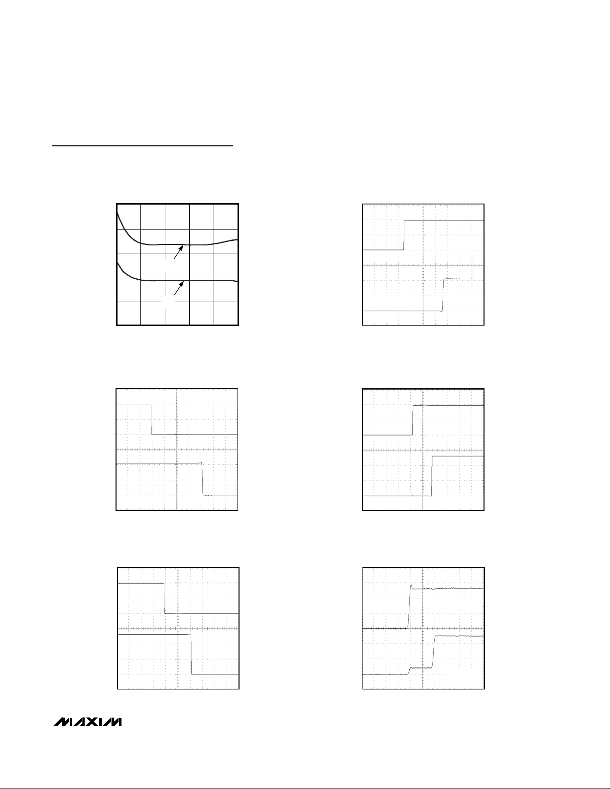
PROPAGATION DELAY vs. V
4.5
4.0
3.5
t
pd-
3.0
PROPAGATION DELAY (µs)
2.5
2.0
021 345
t
pd+
VCM (mV)
PROPAGATION DELAY (tPD-)
IN+
CM
MAX9100 toc10
MAX9100 toc12
50mV/div
PROPAGATION DELAY (tPD+)
IN+
OUT 500mV/div
VOD = 50mV
1µs/div
PROPAGATION DELAY (tPD+)
IN+
MAX9100 toc11
50mV/div
MAX9100 toc13
50mV/div
MAX9100 toc14
500mV/div
50mV/div
2V/div
OUT
V
OUT
CC
VOD = 50mV
1µs/div
POWER-UP DELAY
100ns/div
VIN- = 0
+ = 100mV
V
IN
MAX9100 toc15
OUT
VOD = 50mV
1µs/div
PROPAGATION DELAY (tpd-)
IN+
OUT
VOD = 50mV
1µs/div
2V/div
2V/div
2V/div
Page 6

MAX9100/MAX9101
+1.0V Micropower SOT23 Comparators
6 _______________________________________________________________________________________
Detailed Description
The MAX9100/MAX9101 are low-power and ultra-low
single-supply voltage comparators. They have an operating supply voltage range between +1.0V to +5.5V
and consume only 5µA of quiescent supply current,
while achieving 4µs propagation delay.
Input Stage Circuitry and
Rail-to-Rail Operation
The devices’ input common-mode range is fully specified from 0 to (VCC- 0.2V), although full rail-to-rail input
range is possible with degraded performance. These
comparators may operate at any differential input voltage within these limits. Input bias current is typically
±5nA if the input voltage is within the specified common-mode range. Comparator inputs are protected
from overvoltage by internal diodes connected to the
supply rails. As the input voltage exceeds the supply
rails, these diodes become forward biased and begin
to conduct. Consequently, bias currents increase exponentially as the input voltage exceeds the supply rails.
True rail-to-rail input operation is also possible. For
input common-mode voltages from V
CC
- 0.2V to VCC,
the input bias current will typically increase to 800nA.
Additionally, the supply current will typically increase to
7µA. Otherwise, the device functions as within the
specified common-mode range. See graphs in the
Typical Operating Characteristics.
Output Stage Circuitry
The MAX9100/MAX9101 contain a unique output stage
capable of rail-to-rail operation. Many comparators
consume orders of magnitude more current during
switching than during steady-state operation. However,
with this family of comparators, the supply-current
change during an output transition is extremely small.
The Typical Operating Characteristics graph Supply
Current vs. Output Transition Frequency shows the minimal supply-current increase as the output switching
frequency approaches 100kHz. This characteristic
reduces the requirement for power-supply filter capacitors to reduce glitches created by comparator switching currents. This feature increases battery life in
portable applications.
Push-Pull Output (MAX9100)
The MAX9100 has a push-pull CMOS output. The output stage swings rail-to-rail under no-load conditions.
External load drive capability varies with supply voltage.
SWITCHING CURRENT
OUTPUT RISING
MAX9100 toc16
100mV/div
1mA/div
2µs/div
5V/div
VOD = 50mV
,
SWITCHING CURRENT,
OUTPUT FALLING
MAX9100 toc17
IN+
I
CC
100mV/div
1mA/div
2µs/div
OUT 5V/div
VOD = 50mV
RESPONSE TO SLOW TRIANGLE WAVEFORM
MAX9100 toc18
5.0ms/div
IN+
OUT
50mV/div
2V/div
Typical Operating Characteristics (continued)
(VCC= +5V, VCM= 0, TA= +25°C, unless otherwise noted.)
Pin Description
PIN
SOT23-5 SO-8
1 6 OUT Comparator Output
2 4 GND Ground
3 3 IN+ Noninverting Input
4 2 IN- Inverting Input
— 1, 5, 8 N.C. No Connection
57VCCPositive Supply Voltage
NAME FUNCTION
Page 7
MAX9100/MAX9101
+1.0V Micropower SOT23 Comparators
_______________________________________________________________________________________ 7
Open-Drain Output (MAX9101)
The MAX9101 has an open-drain output, which can be
pulled up to +6.0V above ground independent of the
supply voltage. This is typically used with an external
pullup resistor, facilitating interface between mixed logic
voltages. Alternatively, multiple open-drain comparator
outputs can be connected in a wire-OR configuration.
Applications Information
Low-Voltage Operation: VCC= 1V
The minimum operating voltage is +1.0V. At lower supply voltages, the input common-mode range remains
rail-to-rail, but the comparator’s output drive capability is
reduced and propagation delay increases (see Typical
Operating Characteristics).
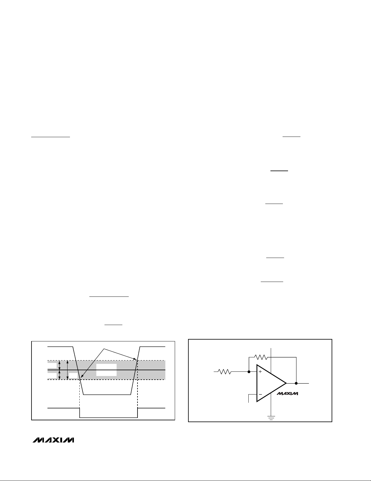
Internal Hysteresis
Hysteresis increases the comparators’ noise margin by
increasing the upper threshold and decreasing the
lower threshold (Figure 1). This hysteresis prevents the
comparator from providing multiple poles when driven
with a very-slow-changing signal.
Additional Hysteresis
These comparators have 1.0mV internal hysteresis.
Additional hysteresis can be generated with two resistors using positive feedback (Figure 2). Use the following procedure to calculate resistor values:
1) Calculate the trip points of the comparator using
these formulas:
and
V
TH
is the threshold voltage at which the comparator
switches its output from high to low as VINrises
above the trip point. VTLis the threshold voltage at
which the comparator switches its output from low to
high as VINdrops below the trip point.
2) The hysteresis band will be:
V
HYS
= VTH- VTL= V
CC
3) In this example, let VCC= +5V and V
REF
= +2.5V:
and
4) Select R2. In this example, we will choose 1kΩ.
5) Select V
HYS
. In this example, we will choose 50mV.
6) Solve for R1:
where R1 ≈ 100kΩ, VTH= 2.525V, and VTL= 2.475V.
Board Layout and Bypassing
A power-supply bypass capacitor is not normally
required, but 100nF bypass capacitors can be used
when the supply impedance is high or when the supply
Figure 1. Threshold Hysteresis Band
Figure 2. Additional Hysteresis (MAX9100)
VV
=+
TH REF
VVR
−
CC REF
()
12
RR
+
2
25 25
V
..
=+
TH
25 1
.
V
=−
TL
RR
2
R
12
RR
+
2
R
12
RR
+
12+
R
2
VV
=
HYS CC
0 050 5
. =
1000
R
1 1000
2
R
12
RR
+
+
VV
=−
TL REF
1
2
R
12
RR
+
V
IN+
VIN - +V
HYST/2
IN-
VIN - V
HYST
OUT
V
HYST
THRESHOLDS
HYSTERESIS
BAND
R2
V
REF
V
IN
CC
R2
V
CC
OUT
GND
MAX9100
Page 8

MAX9100/MAX9101
+1.0V Micropower SOT23 Comparators
leads are long. Minimize signal lead lengths to reduce
stray capacitance between the input and output that
might cause instability.
Typical Application
Logic-Level Translator
3V to 5V
Figure 3 shows an application that converts 3V logic
levels to 5V logic levels. The push-pull output MAX9100
is powered by the +5V supply voltage, and the inverting input is biased to +1.5V with two resistors. This configuration allows a full 5V swing at the output,
maximizing the noise margin of the receiving circuit.
1V to 3V
Figure 4 shows an application that converts 1V logic
levels to 3V logic levels. The MAX9101 is powered by
the +1V supply voltage, and the pullup resistor for the
output is connected to the +3V supply voltage. The
inverting input is biased to +0.5V with two resistors.
Chip Information
TRANSISTOR COUNT: 393
PROCESS: BiCMOS
Figure 3. MAX9100 Logic-Level Translator
Figure 4. MAX9101 Logic-Level Translator
MAX9100
MAX9101
N.C.
IN-
N.C.
V
CC
N.C.
OUT
IN+
GND
SO-8
1
2
3
4
1
8
7
6
5
Pin Configurations (continued)
Maxim cannot assume responsibility for use of any circuitry other than circuitry entirely embodied in a Maxim product. No circuit patent licenses are
implied. Maxim reserves the right to change the circuitry and specifications without notice at any time.
8 _____________________Maxim Integrated Products, 120 San Gabriel Drive, Sunnyvale, CA 94086 408-737-7600
© 2000 Maxim Integrated Products Printed USA is a registered trademark of Maxim Integrated Products.
+5V
232k
100k
IN-
IN+
V
CC
OUT
MAX9100
GND
3V LOGIC IN
5V
LOGIC OUT
+1.0V
100k
100k
IN-
IN+
V
CC
OUT
MAX9101
GND
1V LOGIC IN
+3V
R
PULLUP
3V
LOGIC OUT
 Loading...