

Page 1
For pricing, delivery, and ordering information, please contact Maxim/Dallas Direct! at
1-888-629-4642, or visit Maxim’s website at www.maxim-ic.com.
General Description
The MAX9075/MAX9077 single/dual comparators are
optimized for 3V and 5V single-supply applications.
These comparators have a 580ns propagation delay and
consume just 3µA per comparator. The combination of
low-power, single-supply operation down to 2.1V, and
ultra-small footprint makes these devices ideal for all
portable applications.
The MAX9075/MAX9077 have a common-mode input
voltage range of -0.2V to VCC- 1.2V. Unlike many comparators, there is no differential clamp between the
inputs, allowing the differential input voltage range to
extend Rail-to-Rail®. All inputs and outputs tolerate a
continuous short-circuit fault condition to either rail.
The design of the output stage limits supply-current
surges while switching (typical of many other comparators), minimizing power consumption under dynamic
conditions. Large internal push-pull output drivers allow
rail-to-rail output swing with loads up to 2mA, making
these devices ideal for interface with TTL/CMOS logic.
The MAX9075 single comparator is available in 5-pin
SC70 and SOT23 packages, while the MAX9077 dual
comparator is available in 8-pin SOT23, µMAX, and SO
packages.
Applications
Battery-Powered Systems
Threshold Detectors/Discriminators
Keyless Entry Systems
IR Receivers
Digital Line Receivers
Features
♦ 580ns Propagation Delay from Only 3µA
♦ 2.1V to 5.5V Single-Supply Operation
♦ Ground-Sensing Inputs
♦ Rail-to-Rail Outputs
♦ No Output Phase Inversion for Overdriven Inputs
♦ No Differential Clamp Across Inputs
♦ Available in Ultra-Small Packages
5-Pin SC70 (MAX9075)
8-Pin SOT23 (MAX9077)
MAX9075/MAX9077
Low-Cost, Ultra-Small, 3µA
Single-Supply Comparators
________________________________________________________________ Maxim Integrated Products 1
19-1547; Rev 1; 9/01
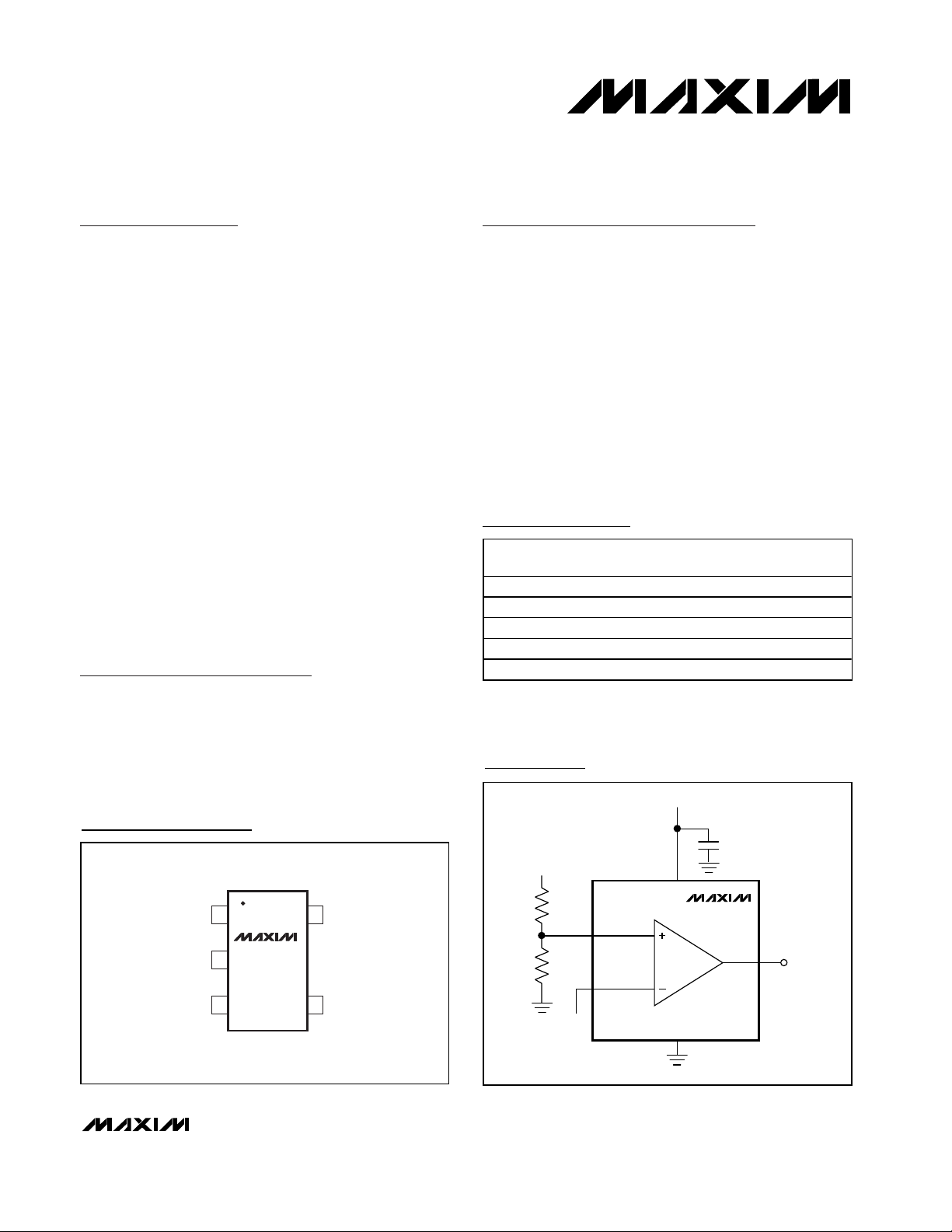
Ordering Information
Typical Operating Circuit
Pin Configurations
Pin Configurations continued at end of data sheet.
Rail-to-Rail is a registered trademark of Nippon Motorola, Ltd.
PART TEMP RANGE
MAX9075EXK-T -40°C to +85°C 5 SC70-5 AAC
MAX9075EXK-T -40°C to +85°C 5 SOT23-5 ADLX
MAX9077EKA-T -40°C to +85°C 8 SOT23-8 AAAD
MAX9077EUA -40°C to +85°C 8 µMAX —
MAX9077ESA -40°C to +85°C 8 SO —
PINPACKAGE
TOP
MARK
V
CC
TOP VIEW
15V
OUT
GND
MAX9075
2
34
SC70-5/SOT23-5
CC
IN-IN+
V
IN
V
CC
IN+
IN-
V
REF
MAX9075
MAX9077
OUT
GND
Page 2
VCC= 5V
MAX9075/MAX9077
Low-Cost, Ultra-Small, 3µA
Single-Supply Comparators
2 _______________________________________________________________________________________
ABSOLUTE MAXIMUM RATINGS
ELECTRICAL CHARACTERISTICS
(VCC= 5V, VCM= -0.2V, TA= T
MIN
to T
MAX
, unless otherwise noted. Typical values are at TA= +25°C.) (Note 1)
Stresses beyond those listed under “Absolute Maximum Ratings” may cause permanent damage to the device. These are stress ratings only, and functional
operation of the device at these or any other conditions beyond those indicated in the operational sections of the specifications is not implied. Exposure to
absolute maximum rating conditions for extended periods may affect device reliability.
Note 1: All devices are 100% production tested at TA= +25°C. All temperature limits are guaranteed by design.
Note 2: Inferred from CMRR. Either input can be driven to the absolute maximum limit without output inversion, as long as the other
input is within the input voltage range.
Note 3: Guaranteed by design.
Supply Voltage
V
CC
to GND........................................................................6V
All Other Pins to GND...........................-0.3V to (V
CC
+ 0.3V)
Duration of Output Short-Circuit to GND or V
CC
........Continuous
Continuous Power Dissipation (T
A
= +70°C)
5-Pin SC70 (derate 2.5mW/°C above +70°C)............200mW
5-Pin SOT23 (derate 7.1mW/°C above +70°C)..........571mW
8-Pin SOT23 (derate 5.3mW/°C above +70°C)..........421mW
8-Pin µMAX (derate 4.5mW/°C above +70°C) ...........362mW
8-Pin SO (derate 5.88mW/°C above +70°C)..............471mW
Operating Temperature Range ...........................-40°C to +85°C
Storage Temperature Range .............................-65°C to +150°C
Lead Temperature (soldering, 10s) .................................+300°C
Inferred from PSRR
C
LOAD
= 10pF
-0.2V ≤ VCM≤ (VCC- 1.2V)
C
LOAD
= 10pF, overdrive = 100mV
C
LOAD
= 10pF, overdrive = 100mV
VCM= 0 (Note 3)
VCC= 3V
2.1V ≤ VCC≤ 5.5V
(Note 2)
I
SINK
= 2mA
I
SOURCE
= 2mA
CONDITIONS
ns
1.6
Rise/Fall Time
ns
250
t
PD-
Propagation Delay High to Low
ns
580
t
PD+
Propagation Delay Low to High
V
0.4
V
OL
OUT_ Output Voltage Low
V
VCC-
0.4
V
OH
OUT_ Output Voltage High
6.6
3 5.2
I
CC
V
2.1 5.5
V
CC
Operating Supply Voltage Range
Supply Current per Comparator
dB
60 82
CMRRCommon-Mode Rejection Ratio
pF
3
C
IN
Input Capacitance
nA-5 -20I
B
Input Bias Current
nA
1
I
OS
Input Offset Current
2.4
dB
54 77
PSRRPower-Supply Rejection Ratio
V
-0.2
V
CC
-
1.2
V
CMR
Common-Mode Voltage Range
mV
±1 ±8
V
OS
Input Offset Voltage
UNITSMIN TYP MAXSYMBOLPARAMETER
TA= +25°C
TA= T
MIN
to T
MAX
VCC= 5V
µA
Page 3
MAX9075/MAX9077
Low-Cost, Ultra-Small, 3µA
Single-Supply Comparators
_______________________________________________________________________________________ 3
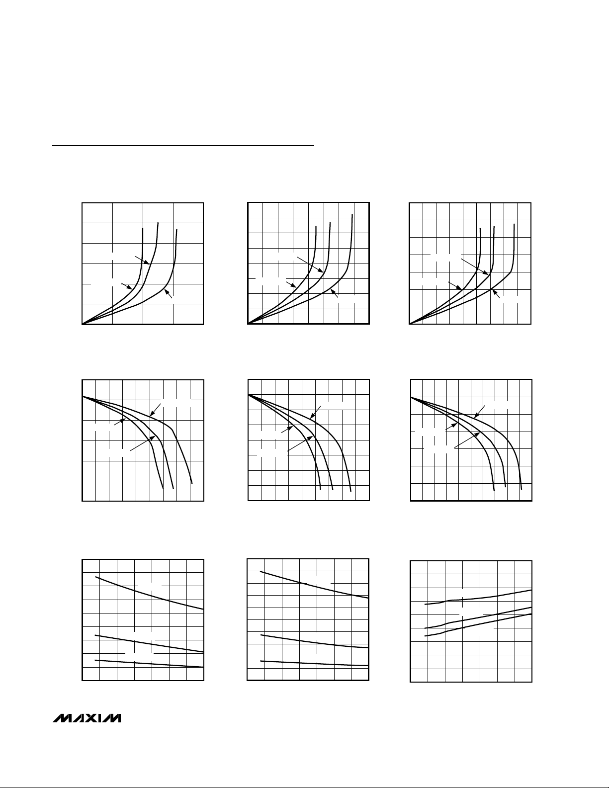
Typical Operating Characteristics
(VCC= 5V, VCM= 0, 100mV overdrive, TA= +25°C, unless otherwise noted.)
OUTPUT VOLTAGE LOW vs.
SINK CURRENT (V
3.0
2.5
2.0
1.5
1.0
OUTPUT VOLTAGE (V)
0.5
0
TA = +25°C
TA = +85°C
01051520
SINK CURRENT (mA)
= 2.1V)
CC
MAX9075/7 toc01
TA = -40°C
OUTPUT VOLTAGE HIGH vs.
SOURCE CURRENT (V
2.5
2.0
1.5
TA = +85°C
1.0
0.5
OUTPUT VOLTAGE (V)
-0.5
TA = +25°C
0
0426810
SOURCE CURRENT (mA)
= 2.1V)
CC
TA = -40°C
12 14 16 18
MAX9075/7 toc04
4.0
3.5
3.0
2.5
2.0
1.5
OUTPUT VOLTAGE (V)
1.0
0.5
3.5
3.0
2.5
2.0
1.5
1.0
OUTPUT VOLTAGE (V)
0.5
-0.5
OUTPUT VOLTAGE LOW vs.
SINK CURRENT (V
TA = +25°C
TA = +85°C
0
0105 152025303540
SINK CURRENT (mA)
CC
OUTPUT VOLTAGE HIGH vs.
SOURCE CURRENT (V
TA = -40°C
TA = +85°C
TA = +25°C
0
0105152025
SOURCE CURRENT (mA)
30 35 40 45
= 3V)
TA = -40°C
= 3V)
CC
7
6
MAX9075/7 toc02
5
4
3
OUTPUT VOLTAGE (V)
2
1
0
6
5
MAX9075/7 toc05
4
3
2
OUTPUT VOLTAGE (V)
1
0
-1
OUTPUT VOLTAGE LOW vs.
SINK CURRENT (V
TA = +25°C
TA = +85°C
02010 30 40 50
SINK CURRENT (mA)
OUTPUT VOLTAGE HIGH vs.
SOURCE CURRENT (V
TA = +85°C
TA = +25°C
02010 30 40 50
SOURCE CURRENT (mA)
= 5V)
CC
TA = -40°C
60 70 80 90
= 5V)
CC
TA = -40°C
60 70 80 90 100
MAX9075/7 toc03
MAX9075/7 toc06
SHORT-CIRCUIT SINK CURRENT
vs. TEMPERATURE
90
80
70
60
50
40
30
SINK CURRENT (mA)
20
10
0
-55 -35 -15 5 25 45 65 85
VCC = 5V
VCC = 3V
VCC = 2.1V
TEMPERATURE (°C)
100
90
MAX9075 toc07
80
70
60
50
40
30
SOURCE CURRENT (mA)
20
10
0
SHORT-CIRCUIT SOURCE CURRENT
vs. TEMPERATURE
VCC = 5V
VCC = 3V
VCC = 2.1V
-55 -35 -15 5 25 45 65 85
TEMPERATURE (°C)
MAX9075 toc08
SUPPLY CURRENT vs.
TEMPERATURE (OUT = HIGH)
4.5
4.0
3.5
3.0
2.5
2.0
1.5
SUPPLY CURRENT (µA)
1.0
0.5
0
-55 -35 -15 5 25 45 65 85
VCC = 5V
VCC = 3V
VCC = 2.1V
TEMPERATURE (°C)
MAX9075 toc09
Page 4

MAX9075/MAX9077
Low-Cost, Ultra-Small, 3µA
Single-Supply Comparators
4 _______________________________________________________________________________________
Typical Operating Characteristics (continued)
(VCC= 5V, VCM= 0, 100mV overdrive, TA= +25°C, unless otherwise noted.)
SUPPLY CURRENT vs.
TEMPERATURE (OUT = LOW)
4.0
3.5
3.0
2.5
2.0
1.5
SUPPLY CURRENT (µA)
1.0
0.5
0
-55 -35 -15 5 25 45 65 85
VCC = 5V
VCC = 3V
VCC = 2.1V
TEMPERATURE (°C)
MAX9075 toc10
PROPAGATION DELAY
vs. LOAD CAPACITANCE
0.7
0.6
0.5
0.4
0.3
0.2
PROPAGATION DELAY (µs)
0.1
0
0 500 1000 1500 2000
t
PD+
t
PD-
LOAD CAPACITANCE (pF)
MAX9075 toc13
SUPPLY CURRENT vs.
OUTPUT TRANSITION FREQUENCY
1000
100
10
SUPPLY CURRENT (µA)
1
1 1k 10k 100k10 100 1M
TRANSITION FREQUENCY (Hz)
VCC = 3V
PROPAGATION DELAY
vs. INPUT OVERDRIVE (t
1.6
1.4
1.2
1.0
0.8
0.6
PROPAGATION DELAY (µs)
0.4
0.2
0
0 50 100 150 200 250
INPUT OVERDRIVE (mV)
VCC = 5V
VCC = 2.1V
PD+
V
= 5V
CC
V
V
CC
CC
= 2.1V
)
= 3V
-0.1
MAX9075 toc11
-0.2
-0.3
-0.4
-0.5
OFFSET VOLTAGE (mV)
-0.6
-0.7
-0.8
MAX9075 toc14
PROPAGATION DELAY (µs)
INPUT OFFSET VOLTAGE
vs. TEMPERATURE
0
VCC = 5V
VCC = 3V
VCC = 2.1V
-55 -35 -15 5 25 45 65 85
TEMPERATURE (°C)
PROPAGATION DELAY
0.7
vs. INPUT OVERDRIVE (t
0.6
0.5
0.4
0.3
0.2
0.1
0
0 50 100 150 200 250
INPUT OVERDRIVE (mV)
PD-
V
= 2.1V
CC
V
= 5V
CC
MAX9075 toc12
)
MAX9075 toc15
V
= 3V
CC
PROPAGATION DELAY
vs. TEMPERATURE (V
500
450
400
350
300
250
200
150
PROPAGATION DELAY (ns)
100
50
0
-55 -35 -15 5 25 45 65 85
= 2.1V)
CC
t
PD+
t
PD-
°
600
500
MAX9075 toc16
400
300
200
PROPAGATION DELAY (ns)
100
0
-55 -35 -15 5 25 45 65 85
PROPAGATION DELAY
vs. TEMPERATURE (V
t
PD+
t
PD-
TEMPERATURE (°C)
CC
= 3V)
800
700
MAX9075 toc17
600
500
400
300
PROPAGATION DELAY (ns)
200
100
0
PROPAGATION DELAY
vs. TEMPERATURE (V
-55 -35 -15 5 25 45 65 85
TEMPERATURE (°C)
= 5V)
CC
t
PD+
t
PD-
MAX9075 toc18
Page 5

MAX9075/MAX9077
Low-Cost, Ultra-Small, 3µA
Single-Supply Comparators
_______________________________________________________________________________________ 5
Typical Operating Characteristics (continued)
(VCC= 5V, VCM= 0, 100mV overdrive, TA= +25°C, unless otherwise noted.)
PROPAGATION DELAY (t
50mV/div
2V/div
100ns/div
PROPAGATION DELAY (t
50mV/div
)
PD+
MAX9075/7 toc19
VCC = 5V
)
PD+
MAX9075/7 toc21
VCC = 3V
V
IN
V
OUT
V
IN
50mV/div
2V/div V
50mV/div
PROPAGATION DELAY (t
100ns//div
PROPAGATION DELAY (t
)
PD-
MAX9075/7 toc20
VCC = 5V
)
PD-
MAX9075/7 toc22
VCC = 3V
V
IN
OUT
V
IN
1V/div
50mV/div
1V/div
100ns/div
V
OUT
1V/div
100ns/div
V
OUT
INPUT BIAS CURRENT
TRIANGLE WAVE
200µs/div
MAX9075/7 toc23
VCC = 3V
7
6
V
IN
V
OUT
5
4
3
2
INPUT BIAS CURRENT (nA)
1
0
-55 -35 -15 5 25 45 65 85
vs. TEMPERATURE
VCC = 5V
VCC = 2.1V
TEMPERATURE (°C)
MAX9075 toc24
VCC = 3V
Page 6

MAX9075/MAX9077
Low-Cost, Ultra-Small, 3µA
Single-Supply Comparators
6 _______________________________________________________________________________________
Pin Description
FUNCTIONNAME
SOT23
MAX9077
µMAX/SOSC70 SOT23
—1 — Comparator OutputOUT1
1— 1
42 2 GroundGND2
Output of Comparator AOUTA—
—3 —
3— 4 Noninverting Input of Comparator AINA+—
—4 —
2— 3 Inverting Input of Comparator AINA-—
Inverting Comparator InputIN-4
Noninverting Comparator InputIN+3
85 8 Positive Supply VoltageV
CC
5
5— 5
6— 6 Inverting Input of Comparator BINB-—
7— 7 Output of Comparator BOUTB—
Noninverting Input of Comparator BINB+—
MAX9075
PIN
Detailed Description
The MAX9075/MAX9077 feature a 580ns propagation
delay from an ultra-low supply current of only 3µA per
comparator. These devices are capable of single-supply operation in the 2.1V to 5.5V range. Large internal
output drivers allow rail-to-rail output swing with up to
2mA loads. Both comparators offer a push-pull output
that sinks and sources current.
Comparator Output
The MAX9075/MAX9077 are designed to maintain a
low-supply current during repeated transitions by limiting the shoot-through current.
Noise Considerations, Comparator Input
The input common-mode voltage range for these
devices extends from -0.2V to V
CC
- 1.2V. Unlike many
other comparators, the MAX9075/MAX9077 can operate at any differential input voltage within these limits.
Input bias current is typically -5nA if the input voltage is
between the supply rails.
Although the comparators have a very high gain, useful
gain is limited by noise. The comparator has a wideband peak-to-peak noise of approximately 70µV.
Applications Information
Adding Hysteresis
Hysteresis extends the comparator’s noise margin by
increasing the upper threshold and decreasing the
lower threshold. A voltage divider from the output of the
comparator sets the trip voltage. Therefore, the trip
voltage is related to the output voltage. Set the hysteresis with three resistors using positive feedback, as
shown in Figure 1.
The design procedure is as follows:
1) Choose R3. The leakage current of IN+ may cause a
small error; however, the current through R3 can be
approximately 500nA and still maintain accuracy.
The added supply current due to the circuit at the
trip point is V
CC
/R3; 10MΩ is a good practical value
for R3, as this keeps the current well below the supply current of the chip.
2) Choose the hysteresis voltage (V
HYS
), which is the
voltage between the upper and lower thresholds. In
this example, choose V
HYS
= 50mV and assume
V
REF
= 1.2V and VCC= 5V.
3) Calculate R1 as follows:
R1 = R3 · V
HYS
/ VCC= 10MΩ · 0.05 / 5 = 100kΩ
Page 7

4) Choose the threshold voltage for VINrising (V
THR
). In
this example, choose V
THR
= 3V.
5) Calculate R2 as follows:
R2 = 1 / {[V
THR
/ (V
REF
✕ R1)] - 1/R1 - 1/R3} =
1 / {[3 / (1.2 ✕ 100kΩ)] - 1/100kΩ - 1/10MΩ} = 67.114kΩ
A 1% preferred value is 64.9kΩ.
6) Verify the threshold voltages with these formulas:
V
IN
rising:
V
THR
= V
REF
✕ R1 (1/R1 + 1/R2 + 1/R3)
V
IN
falling:
V
THF
= V
THR
- (R1 ✕ VCC) / R3
7) Check the error due to input bias current (5nA). If the
error is too large, reduce R3 and recalculate.
V
TH
= IB(R1 ✕ R2 ✕ R3) / (R1 + R2 + R3) = 0.2mV
Board Layout and Bypassing
Use 10nF power-supply bypass capacitors. Use 100nF
bypass capacitors when supply impedance is high,
when supply leads are long, or when excessive noise is
expected on the supply lines. Minimize signal trace
lengths to reduce stray capacitance. Minimize the
capacitive coupling between IN- and OUT. For slowmoving input signals (rise time > 1ms) use a 1nF
capacitor between IN+ and IN-.
Chip Information
MAX9075 TRANSISTOR COUNT: 86
MAX9077 TRANSISTOR COUNT: 142
MAX9075/MAX9077
Low-Cost, Ultra-Small, 3µA
Single-Supply Comparators
_______________________________________________________________________________________ 7
Figure 1. Adding Hysteresis
INB-
INB+INA+
1
2
87V
CC
OUTB
GND
INA-
OUTA
SOT23-8
TOP VIEW
3
4
6
5
INB-
INB+GND
1
2
87V
CC
OUTBINA-
INA+
OUTA
µMAX/SO
3
4
6
5
MAX9077
MAX9077
Pin Configurations (continued)
V
CC
R3
R1
V
IN
R2
V
REF
V
GND
CC
OUT
MAX9075
MAX9077
Page 8

MAX9075/MAX9077
Low-Cost, Ultra-Small, 3µA
Single-Supply Comparators
Maxim cannot assume responsibility for use of any circuitry other than circuitry entirely embodied in a Maxim product. No circuit patent licenses are
implied. Maxim reserves the right to change the circuitry and specifications without notice at any time.
8 _____________________Maxim Integrated Products, 120 San Gabriel Drive, Sunnyvale, CA 94086 408-737-7600
© 2001 Maxim Integrated Products Printed USA is a registered trademark of Maxim Integrated Products.
Package Information
(The package drawing(s) in this data sheet may not reflect the most current specifications. For the latest package outline information,
go to www.maxim-ic.com/packages.)
SC70, 5L.EPS
SOT23, 8L.EPS
 Loading...