

Page 1
General Description
The MAX9039–MAX9043 and MAX9050–MAX9053 feature combinations of low-power comparators and precision voltage references. Their operating voltage range
makes them ideal for both 3V and 5V systems. The
MAX9039/MAX9040/MAX9041/MAX9050/MAX9051
have a single comparator and reference consuming
only 40µA of supply current. The MAX9042/MAX9043/
MAX9052/MAX9053 have dual comparators and one
reference, and consume only 55µA of supply current.
Low-voltage operation and low supply current make
these devices ideal for battery-operated systems.
The comparators feature Rail-to-Rail
®
inputs and outputs, with a common-mode input voltage range that
extends 250mV beyond the supply rails. Input bias current is typically 1.0pA, and input offset voltage is typically 0.5mV. Internal hysteresis ensures clean output
switching, even with slow-moving input signals. The
output stage features a unique design that limits supply
current surges while switching, virtually eliminating supply glitches typical of many other comparators. This
design also minimizes overall power consumption
under dynamic conditions. The comparator outputs
have rail-to-rail, push-pull output stages that sink and
source up to 8mA. The propagation delay is 400ns,
even with the low-operating supply current.
The reference output voltage is set to 1.23V in the
MAX9039, to 2.048V in the MAX9040–MAX9043, and to
2.500V in the MAX9050–MAX9053. The MAX9040–
MAX9043 and the MAX9050–MAX9053 are offered in
two grades: an A grade with 0.4% initial accuracy and
6ppm/°C tempco, and a B grade with 1% initial accuracy and 100ppm/°C tempco. The voltage references
feature a proprietary curvature-correction circuit and
laser-trimmed thin-film resistors. These series-mode references can sink or source up to 500µA of load current.
Applications
Features
♦ Comparator + Precision Reference in UCSP/SOT23
♦ 2.5V to 5.5V Single-Supply Operation
(MAX9039–MAX9043)
♦ Low Supply Current (MAX9039/MAX9040/
MAX9041/MAX9050/MAX9051)
40µA Quiescent
50µA with 100kHz Switching
♦ 400ns Propagation Delay
♦ Rail-to-Rail Inputs
♦ Rail-to-Rail Output Stage Sinks and Sources 8mA
♦ Internal ±3mV Hysteresis
♦ Voltage Reference Offers:
±0.4% (max) Initial Accuracy (A grade)
6ppm/°C (typ) Temperature Coefficient (A grade)
Stable for 0 to 4.7nF Capacitive Loads
MAX9039–MAX9043/MAX9050–MAX9053
Micropower, Single-Supply, UCSP/SOT23
Comparator + Precision Reference ICs
________________________________________________________________ Maxim Integrated Products 1
19-1569; Rev 4; 10/02
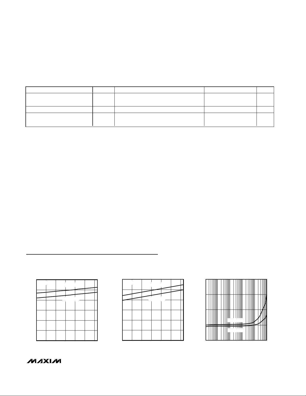
Ordering Information
Rail-to-Rail is a registered trademark of Nippon Motorola, Ltd.
UCSP is a trademark of Maxim Integrated Products, Inc.
*UCSP reliability is integrally linked to the user’s assembly
methods, circuit board material, and environment. Refer to the
UCSP Reliability section of this data sheet for more information.
Typical Operating Circuit and Functional Diagrams appear
at end of data sheet.
Ordering Information continued at end of data sheet.
Selector Guide appears at end of data sheet.
Pin Configurations
Pin Configurations continued at end of data sheet.
For pricing, delivery, and ordering information, please contact Maxim/Dallas Direct! at
1-888-629-4642, or visit Maxim’s website at www.maxim-ic.com.
PINPACKAGE
6 UCSP-6
5 SOT23-5
6 SOT23-6
6 SOT23-6
8 SO
8 SO
5 SOT23-5-40°C to +85°C
MAX9040AEUK-T
ADNW
-40°C to +85°C
-40°C to +85°C
-40°C to +85°C
-40°C to +85°C
-40°C to +85°C
-40°C to +85°C
TEMP RANGEPART
MAX9039BEBT-T*
MAX9040BEUK-T
MAX9041AEUT-T
MAX9041BEUT-T
MAX9041AESA
MAX9041BESA
TOP
MARK
AAZ
ADNX
AAHF
AAHH
—
—
Precision Battery
Management
Window Comparators
IR Receivers
Level Translators
Digital Line Receivers
TOP VIEW (BUMPS ON BOTTOM) TOP VIEW
B1
IN+
MAX9039
B2
IN-
B3
REF
UCSP
A1
V
EE
OUT
A2
A3
V
CC
15V
OUT
V
MAX9040
2
EE
MAX9050
34
SOT23-5
CC
REFIN+
Page 2
MAX9039–MAX9043/MAX9050–MAX9053
Micropower, Single-Supply, UCSP/SOT23
Comparator + Precision Reference ICs
2 _______________________________________________________________________________________
ABSOLUTE MAXIMUM RATINGS
ELECTRICAL CHARACTERISTICS—A Grade (0.4% Initial Accuracy)
(VCC= +5V, VEE= 0V, VCM= 0V, I
OUT
= 0A, I
REF
= 0A, TA= T
MIN
to T
MAX
, unless otherwise noted. Typical values are at
T
A
= +25°C.) (Note 2)
Stresses beyond those listed under “Absolute Maximum Ratings” may cause permanent damage to the device. These are stress ratings only, and functional
operation of the device at these or any other conditions beyond those indicated in the operational sections of the specifications is not implied. Exposure to
absolute maximum rating conditions for extended periods may affect device reliability.
Supply Voltage (VCCto VEE) ....................................-0.3V to +6V
All Other Pins ...................................(V
EE
- 0.3V) to (VCC+ 0.3V)
Output Short-Circuit Duration
(OUT_, REF) ...............Indefinite Short Circuit to Either Supply
Continuous Power Dissipation (T
A
= +70°C)
5-Pin SOT23 (derate 7.10mW/°C above +70°C)..........571mW
6-Bump UCSP (derate 3.9mW/°C above +70°C) ........308mW
6-Pin SOT23 (derate 8.70mW/°C above +70°C)..........696mW
8-Pin SO (derate 5.88mW/°C above +70°C)................471mW
8-Pin µMAX (derate 4.1mW/°C above +70°C) .............330mW
10-Pin µMAX (derate 5.6mW/°C above +70°C) ...........444mW
Operating Temperature Range ...........................-40°C to +85°C
Junction Temperature......................................................+150°C
Storage Temperature Range .............................-65°C to +150°C
Lead Temperature (soldering, 10s) .................................+300°C
Bump Reflow Temperature (Note 1) ................................+235°C
Note 1: This device is constructed using a unique set of packaging techniques that impose a limit on the thermal profile the device
can be exposed to during board-level solder attach and rework. This limit permits only the use of the solder profiles recommended in the industry-standard specification, JEDEC 020A, paragraph 7.6, Table 3 for IR/VPR and Convection Packaging
Reflow. Preheating is required. Hand or wave soldering is not allowed.
PARAMETER SYMBOL CONDITIONS MIN TYP MAX UNITS
Supply Voltage Range (Note 3) V
Supply Current I
COMPARATORS
Input Offset Voltage (Note 4) V
Input Hysteresis V
Input Bias Current
(Notes 5, 6, 7)
Input Offset Current (Note 5) I
Common-Mode Voltage Range
(Notes 5, 8)
Common-Mode Rejection Ratio
(Note 5)
Power-Supply Rejection Ratio PSRR
Input Capacitance (Note 5) C
Output Short-Circuit Current I
Output Voltage Low V
CC
MAX9040–MAX9043 2.5 5.5
MAX9050–MAX9053 2.7 5.5
MAX9040/MAX9041/
MAX9050/MAX9051
CC
MAX9042/MAX9043/
MAX9052/MAX9053
Over entire
OS
common-mode
range
HYST
I
OS
CMVR
Specified common-mode range ±0.001 ±10.0 nA
B
Specified common-mode range ±0.5 pA
TA = +25°C
T
= -40°C to +85°CV
A
CMRR Specified common-mode range 52 80 dB
MAX9040–MAX9043, 2.5V ≤ VCC ≤ 5.5V 55 80
MAX9050–MAX9053, 2.5V ≤ V
IN
V
V
SC
OL
OUT
VCC = 5V, I
VCC = 2.7V, I
or V
EE
=
SINK
SINK
VCC = 2.7V 47 67
V
= 5V 52 72
CC
VCC = 2.7V 55 80
= 5V 60 85
V
CC
TA = +25°C ±0.5 ±5.0
T
= -40°C to +85°C ±7.0
A
±3.0 mV
V
-
EE
0.25
EE
≤ 5.5V 55 80
CC
VCC +
0.25
V
CC
2.5 pF
CC
VCC = 5V 95
VCC = 2.7V 35
= 8mA 0.2 0.55
= 3.5mA 0.15 0.4
V
µA
mV
V
dB
mA
V
Page 3
MAX9039–MAX9043/MAX9050–MAX9053
Micropower, Single-Supply, UCSP/SOT23
Comparator + Precision Reference ICs
_______________________________________________________________________________________ 3
ELECTRICAL CHARACTERISTICS—A Grade (0.4% Initial Accuracy) (continued)
(VCC= +5V, VEE= 0V, VCM= 0V, I
OUT
= 0A, I
REF
= 0A, TA= T
MIN
to T
MAX
, unless otherwise noted. Typical values are at
T
A
= +25°C.) (Note 2)
ELECTRICAL CHARACTERISTICS—B Grade (1% Initial Accuracy)
(VCC= 5V, VEE= 0V, VCM= 0V, I
OUT
= 0A, I
REF
= 0A, TA= T
MIN
to T
MAX
, unless otherwise noted. Typical values are at TA= +25°C.)
(Note 2)
PARAMETER SYMBOL CONDITIONS MIN TYP MAX UNITS
Output Voltage High V
Output Propagation Delay
(Note 9)
Power-Up Time t
VOLTAGE REFERENCE
Output Voltage V
Output Voltage Temperature
Coefficient (Note 10)
Line Regulation
Load Regulation
Output Short-Circuit Current I
Thermal Hysteresis (Note 11) T
Long-Term Stability 1000h at TA = +25°C 50 ppm
Noise Voltage E
Ripple Rejection
Turn-On Settling Time tR(V
Capacitive-Load Stability Range
(Note 7)
t
PD+/
t
TCV
∆V
∆V
∆V
∆I
HYST
∆V
∆V
C
L(VREF
OH
VCC = 5V, I
VCC = 2.7V, I
= 8mA 4.45 4.85
SOURCE
= 3.5mA 2.3 2.55
SOURCE
CL = 15pF 40
CL = 50pF 50Output Rise/Fall Times tR/t
F
CL = 200pF 80
50mV overdrive 450
100mV overdrive 400
MAX9040–MAX9043 2.040 2.048 2.056
MAX9050–MAX9053 2.490 2.500 2.510
≤ 500µA 2 4
≤ 0µA 3.5 6
REF
4mA
PD-
PU
REF
REF
CC
REF
REF
SC
CL = 15pF,
V
= 2.7V
CC
Time to V
valid logic state 20 µs
OUT
TA = +25°C
µMAX/SO 6 30
REF
SOT23 6 50
2.5V ≤ VCC ≤ 5.5V, MAX9040–MAX9043 +50 +200
/
2.7V ≤ VCC ≤ 5.5V, MAX9050–MAX9053 +50 +200
Sourcing. 0µA ≤ I
/
REF
Sinking, -500µA ≤ I
V
= VEE or V
REF
CC
130 ppm
OUT
REF
f = 0.1Hz to 10Hz 40 µV
f = 10Hz to 10kHz 105 µV
/
VCC = 5V ±100mV, f = 120Hz 84 dB
CC
REF
) To V
= 1% of final value 200 µs
REF
) 0 4.7 nF
V
ns
ns
V
ppm/°C
µV/V
µV/µA
P-P
RMS
PARAMETER SYMBOL CONDITIONS MIN TYP MAX UNITS
Supply Voltage Range (Note 3) V
Supply Current I
CC
CC
MAX9039–MAX9043 2.5 5.5
MAX9050–MAX5053 2.7 5.5
MAX9039/MAX9040/
MAX9041/MAX9050/
MAX9051
MAX9042/MAX9043/
MAX9052/MAX5053
VCC = 2.7V 40
= 5.0V 45 100
V
CC
VCC = 2.7V 55
= 5.0V 60 130
V
CC
V
µA
Page 4
MAX9039–MAX9043/MAX9050–MAX9053
Micropower, Single-Supply, UCSP/SOT23
Comparator + Precision Reference ICs
4 _______________________________________________________________________________________
ELECTRICAL CHARACTERISTICS—B Grade (1% Initial Accuracy) (continued)
(VCC= 5V, VEE= 0V, VCM= 0V, I
OUT
= 0A, I
REF
= 0A, TA= T
MIN
to T
MAX
, unless otherwise noted. Typical values are at TA= +25°C.)
(Note 2)
PARAMETER SYMBOL CONDITIONS MIN TYP MAX UNITS
COMPARATOR
Input Offset Voltage (Note 4) V
Input Hysteresis V
Input Bias Current (Notes 5, 6, 7) I
Input Offset Current (Note 5) I
Common-Mode Voltage Range
(Notes 5, 8)
Common-Mode Rejection Ratio
(Note 5)
Power-Supply Rejection Ratio PSRR
Input Capacitance (Note 5) C
Output Short-Circuit Current I
Output Voltage Low V
Output Voltage High V
Output Propagation Delay
(Note 9)
Power-Up Time t
VOLTAGE REFERENCE
Output Voltage Temperature
Coefficient (Note 10)
Line Regulation
Load Regulation
Output Short-Circuit Current I
Thermal Hysteresis (Note 11) T
Long-Term Stability 1000h at TA = +25°C 100 ppm
Noise Voltage E
OS
HYST
OS
CMVR V
Over entire common-mode range ±1 ±9.0 mV
±3.0 mV
Specified common-mode range ±0.001 ±25.0 nA
B
Specified common-mode range ±0.5 pA
EE
V
CMRR Specified common-mode range 52 80 dB
MAX9039–MAX9043, 2.5V ≤ VCC ≤ 5.5V 55 80
SC
OL
OH
MAX9050–MAX9053, 2.7V ≤ V
IN
V
OUT
VCC = 5V, I
= V
EE
or V
SINK
VCC = 2.7V, I
VCC = 5V, I
SOURCE
VCC = 2.7V, I
VCC = 5V 95
CC
VCC = 2.7V 35
= 8mA 0.2 0.55
= 3.5mA 0.15
SINK
= 8mA 4.45 4.85
= 3.5mA 2.55
SOURCE
≤ 5.5V 55 80
CC
2.5 pF
CL = 15pF 40
CL = 50pF 50Output Rise/Fall Times tR/t
F
CL = 200pF 80
t
PD+/tPD-
PU
CL = 15pF,
V
= 2.7V
CC
Time to V
valid logic state 20 µs
OUT
50mV overdrive 450
100mV overdrive 400
MAX9039 1.218 1.230 1.242
REF
TA = +25°C
MAX9040–MAX9043 2.028 2.048 2.068Output Voltage V
MAX9050–MAX9053 2.475 2.500 2.525
TCV
REF
∆V
/
REF
∆V
∆V
REF
∆I
REF Sinking: -500µA ≤ I
SC
HYST
OUT
2.5V ≤ VCC ≤ 5.5V
CC
Sourcing: 0µA ≤ I
/
V
= VEE or V
REF
f = 0.1Hz to 10Hz 40 µV
f = 10Hz to 10kHz 105 µV
MAX9039–MAX9043 +50 +200
MAX9050–MAX9053 +50 +200
≤ 500µA 2 4
REF
≤ 0µA 3.5 6
REF
CC
20 100 ppm/°C
4mA
130 ppm
CC
V
dB
mA
V
V
ns
ns
V
µV/V
µV/µA
P-P
RMS
Page 5
MAX9039–MAX9043/MAX9050–MAX9053
Micropower, Single-Supply, UCSP/SOT23
Comparator + Precision Reference ICs
_______________________________________________________________________________________ 5
ELECTRICAL CHARACTERISTICS—B Grade (1% Initial Accuracy) (continued)
(VCC= 5V, VEE= 0V, VCM= 0V, I
OUT
= 0A, I
REF
= 0A, TA= T
MIN
to T
MAX
, unless otherwise noted. Typical values are at TA= +25°C.)
(Note 2)
Note 2: All devices are 100% production tested at T
A
= +25°C. Limits over the extended temperature range are guaranteed by
design.
Note 3: Supply voltage range guaranteed by PSRR test on comparator and line regulation of REF.
Note 4: V
OS
is defined as the center of the input-referred hysteresis band.
Note 5: For the comparators with the inverting input (IN-) uncommitted.
Note 6: Input bias current is the average of the inverting and noninverting input bias currents.
Note 7: Not production tested. Guaranteed by design.
Note 8: Guaranteed by CMRR test.
Note 9: V
OVERDRIVE
is beyond the offset and hysteresis determined trip point.
Note 10: Temperature coefficient is measured by the box method; i.e., the maximum ∆V
REF
is divided by the maximum ∆T.
Note 11: Thermal hysteresis is defined as the change in V
REF
at +25°C before and after cycling the device from T
MIN
to T
MAX
.
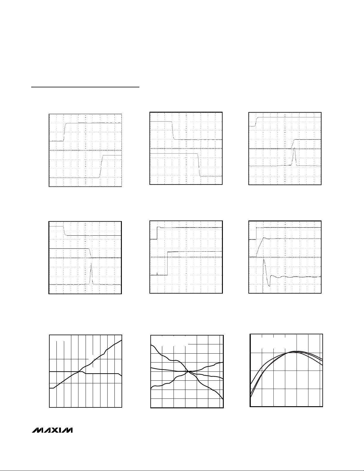
Typical Operating Characteristics
(VCC= 5V, VEE= 0V, VCM= 0V, I
OUT
= 0A, I
REF
= 0A, TA= +25°C, unless otherwise noted.)
0
10
30
20
50
40
60
-40 0-20 20 40 60 80
MAX9039/MAX9040/MAX9041/MAX9050/MAX9051
SUPPLY CURRENT vs. TEMPERATURE
MAX9039/43/50-53 toc01
TEMPERATURE (°C)
SUPPLY CURRENT (µA)
VCC = 5.0V
V
IN+ > VIN-
VCC = 2.7V
0
10
30
20
50
40
60
-40 0-20 20 40 60 80
MAX9042/MAX9043/MAX9052/MAX9053
SUPPLY CURRENT vs. TEMPERATURE
MAX9039/43/50-53 toc02
TEMPERATURE (°C)
SUPPLY CURRENT (µA)
VCC = 5.0V
V
IN+ > VIN-
VCC = 2.7V
0.01 0.1 1 10 100 1000
200
150
100
50
0
MAX9039/MAX9040/MAX9041/MAX9050/MAX9051
SUPPLY CURRENT vs. SWITCHING FREQUENCY
MAX9039/43/50-53 toc03
SWITCHING FREQUENCY (kHz)
SUPPLY CURRENT (µA)
VCC = 5.0V
VCC = 2.7V
PARAMETER SYMBOL CONDITIONS MIN TYP MAX UNITS
Ripple Rejection
Turn-On Settling Time tR(V
Capacitive Load Stability Range
(Note 7)
∆V
∆V
C
L(VREF
REF
CC
REF
/
VCC = 5V ±100mV, f = 120Hz 84 dB
) To V
= 1% of final value 200 µs
REF
) 0 4.7 nF
Page 6

MAX9039–MAX9043/MAX9050–MAX9053
Micropower, Single-Supply, UCSP/SOT23
Comparator + Precision Reference ICs
6 _______________________________________________________________________________________
Typical Operating Characteristics (continued)
(VCC= 5V, VEE= 0V, VCM= 0V, I
OUT
= 0A, I
REF
= 0A, TA= +25°C, unless otherwise noted.)
250
0.01 0.1 1 10 100 1000
200
150
100
50
0
MAX9042/MAX9043/MAX9052/MAX9053
SUPPLY CURRENT vs. SWITCHING FREQUENCY
MAX9039/43/50-53 toc04
SWITCHING FREQUENCY (kHz)
SUPPLY CURRENT (µA)
VCC = 5.0V
VCC = 2.7V
10,000
1000
100
10
1
0.1
0.01 1 100.1
OUTPUT LOW VOLTAGE
vs. OUTPUT SINK CURRENT
MAX9039/43/50-53 toc05
OUTPUT SINK CURRENT (mA)
V
OL
(mV)
VCC = 5.0V
V
IN+ < VIN-
VCC = 2.7V
OUTPUT HIGH VOLTAGE
vs. OUTPUT SOURCE CURRENT
10,000
V
IN+ > VIN-
) (mV)
1000
OH
- V
CC
(V
100
10
1
OUTPUT HIGH VOLTAGE
0.1
0.01 1 100.1
OUTPUT SOURCE CURRENT (mA)
VCC = 2.7V
MAX9039/43/50-53 toc06
VCC = 5.0V
OUTPUT SHORT-CIRCUIT CURRENT
vs. TEMPERATURE
120
100
80
60
40
OUTPUT SINK CURRENT (mA)
20
0
-40 0-20 20 40 60 80
V
IN+ > VIN-
OUT SHORTED TO V
VCC = 5.0V
VCC = 2.7V
TEMPERATURE (°C)
EE
MAX9039/43/50-53 toc07
PROPAGATION DELAY
vs. CAPACITIVE LOAD (V
650
VOD = 50mV
600
550
500
(ns)
PD
t
450
400
t
TO V
PD+
OF FINAL VALUE
t
PD+
OF FINAL VALUE
t
TO V
PD-
OUT
OF FINAL VALUE
TO V
= 50%
350
300
0 400200 600 800100 500300 700 900 1000
CAPACITIVE LOAD (pF)
= 5V)
CC
= 50%
OUT
= 10%
OUT
t
TO V
PD-
OUT
OF FINAL VALUE
MAX9039/43/50-53 toc10
= 10%
OUTPUT SHORT-CIRCUIT CURRENT
vs. TEMPERATURE
100
80
60
40
OUTPUT SOURCE CURRENT (mA)
20
0
-40 -20 0 20 40 60 80
V
IN- > VIN+
OUT SHORTED TO V
TEMPERATURE (°C)
PROPAGATION DELAY
vs. TEMPERATURE
650
VOD = 50mV
600
550
500
(ns)
t
TO V
PD+
PD
t
450
OF FINAL VALUE
400
350
300
-40 0-20 20 40
t
TO V
PD+
OF FINAL VALUE
= 10%
OUT
t
TO V
PD-
OF FINAL VALUE
TEMPERATURE (°C)
OUT
t
TO V
PD-
OF FINAL VALUE
OUT
VCC = 5.0V
VCC = 2.7V
= 50%
OUT
= 10%
60
= 50%
CC
MAX9039/43/50-53 toc08
MAX9039/43/50-53 toc10a
80
(ns)
t
(ns)
PD
t
PROPAGATION DELAY
vs. CAPACITIVE LOAD (V
600
VOD = 50mV
550
500
PD
450
400
350
t
TO V
PD+
= 50%
OUT
OF FINAL VALUE
0 400200 600 800100 500300 700 900 1000
CAPACITIVE LOAD (pF)
CC
t
TO V
PD-
OF FINAL VALUE
t
TO V
PD+
OF FINAL VALUE
t
TO V
PD-
OF FINAL VALUE
PROPAGATION DELAY
vs. INPUT OVERDRIVE
900
800
700
600
500
400
t
, VCC = 5.0V
PD-
300
200
08040 120 16020 10060 140 180 200
t
, VCC = 5.0V
PD+
t
, VCC = 2.7V
PD+
t
, VCC = 2.7V
PD-
INPUT OVERDRIVE (mV)
= 2.7V)
= 50%
OUT
= 10%
OUT
= 10%
OUT
MAX9039/43/50-53 toc09
MAX9039/43/50-53 toc10b
Page 7
MAX9039–MAX9043/MAX9050–MAX9053
Micropower, Single-Supply, UCSP/SOT23
Comparator + Precision Reference ICs
_______________________________________________________________________________________ 7
)
Typical Operating Characteristics (continued)
(VCC= 5V, VEE= 0V, VCM= 0V, I
OUT
= 0A, I
REF
= 0A, TA= +25°C, unless otherwise noted.)
B
A
100ns/div
PROPAGATION DELAY (t
PD+
)
MAX9039/43/50-53 toc11
A = IN+, 50mV/div
B = OUT, 2V/div
B
A
100ns/div
PROPAGATION DELAY (t
PD-
)
MAX9039/43/50-53 toc12
A = IN+, 50mV/div
B = OUT, 2V/div
B
C
A
100ns/div
SWITCHING CURRENT (OUT RISING EDGE)
MAX9039/43/50-53 toc13
A = IN+, 100mV/div
B = OUT, 5V/div
C = I
CC
, 1mA/div
SWITCHING CURRENT (OUT FALLING EDGE)
A
B
MAX9039/43/50-53 toc14
POWER-UP DELAY (OUT)
A
MAX9039/43/50-53 toc15
A
B
POWER-UP DELAY (REF)
MAX9039/43/50-53 toc16
C
A = IN+, 100mV/div
B = OUT, 5V/div
, 1mA/div
C = I
CC
100ns/div
INPUT BIAS CURRENT
vs. INPUT VOLTAGE
0.003
V
= 2.0V
IN-
0.002
0.001
INPUT BIAS CURRENT (nA)
0
0 2.01.50.5 1.0 2.5 3.0 3.5 4.0 4.5 5.0
V
(V)
IN+
I
B+
I
B-
B
A = VCC, 2V/div
B = OUT, 1V/div
1.00
THREE TYPICAL PARTS
NORMALIZED TO +25°C
0.75
0.50
MAX9039/43/50-53 tco17
0.25
0
-0.25
-0.50
OUTPUT VOLTAGE CHANGE (mV)
-0.75
-1.00
-40 0-20 20 40 60 80
5µs/div
MAX904_/MAX905_
REFERENCE OUTPUT VOLTAGE
TEMPERATURE DRIFT
TEMPERATURE (°C
C
A = VCC, 2V/div
B = REF, 1V/div
C = REF, 50mV/div, 2.048V OFFSET
REFERENCE OUTPUT VOLTAGE
1
THREE TYPICAL PARTS
NORMALIZED TO +25°C
MAX9039/43/50-53 toc18
0
-1
-2
OUTPUT VOLTAGE CHANGE (mV)
-3
-40
100µs/div
MAX9039
TEMPERATURE DRIFT
20
0-20
TEMPERATURE (°C)
40
MAX9039/43/50-53 toc19
8060
Page 8

-1500
-500
-1000
500
0
1500
1000
2000
-500 -100-300 100 300 500
LOAD REGULATION
MAX9039/43/50-53 toc21
LOAD CURRENT (µA)
REFERENCE OUTPUT VOLTAGE CHANGE (µV)
TA = +25°C
TA = +85°C
TA = -40°C
MAX9039–MAX9043/MAX9050–MAX9053
Micropower, Single-Supply, UCSP/SOT23
Comparator + Precision Reference ICs
8 _______________________________________________________________________________________
Pin Description
-200
-100
-150
0
-50
100
50
150
2.5 3.5 4.03.0 4.5 5.0 5.5
LINE REGULATION
MAX9039/43/50-53 toc20
INPUT VOLTAGE (V)
REFERENCE OUTPUT VOLTAGE CHANGE (µV)
TA = +25°C
TA = +85°C
TA = -40°C
Typical Operating Characteristics (continued)
(VCC= 5V, VEE= 0V, VCM= 0V, I
OUT
= 0A, I
REF
= 0A, TA= +25°C, unless otherwise noted.)
FUNCTION
MAX9042
MAX9052
MAX9039
MAX9043
MAX9053
Comparator Output
Negative Supply Voltage
Comparator Noninverting Input
Reference Voltage Output
Comparator A Output
No Connection. Not internally connected.
Comparator Inverting Input
Positive Supply Voltage
Comparator A Inverting Input
Comparator B Output
Comparator B Inverting Input
Comparator B Noninverting Input
Comparator A Noninverting Input
NAME
SO
6
4
3
1
—
5, 8
2
7
—
—
—
—
—
SO/µMAX
—
4
—
2
1
—
—
8
—
7
6
5
3
OUT
V
EE
IN+
REF
OUTA
N.C.
IN-
V
CC
INA-
OUTB
INB-
INB+
INA+
SOT23 µMAX
A2 1 —
A1 2 5
UCSP
B1 3 —
B3 5 2
— — 1
— — 9
B2 4 —
A3 6 10
— — 3
— — 8
— — 7
— — 6
— — 4
MAX9041
MAX9051
PIN
MAX9040
MAX9050
1
2
SOT23
3
4
—
—
—
5
—
—
—
—
—
Page 9

Detailed Description
The MAX9039–MAX9043 and MAX9050–MAX9053 feature single/dual, low-power, low-voltage comparators
and a precision voltage reference. They operate from a
single 2.5V to 5.5V (MAX9039/MAX904_) or 2.7V to
5.5V (MAX905_) supply. The single comparators with
reference, (MAX9039/MAX9040/MAX9041/MAX9050/
MAX9051 consume only 40µA of supply current, while
the dual comparators with reference (MAX9042/
MAX9043/MAX9052/MAX9053) consume only 55µA of
supply current. Their common-mode input range
extends 0.25V beyond each rail. Internal hysteresis
ensures clean output switching, even with slow-moving
input signals.
The output stage employs a unique design that minimizes supply current surges while switching, virtually
eliminating the supply glitches typical of many other
comparators. Large internal output drivers allow rail-torail output swing that can sink and source up to 8mA of
current.
The precision reference uses a proprietary curvaturecorrection circuit and laser-trimmed thin-film resistors,
resulting in a temperature coefficient of less than 30ppm/°C
over the extended temperature range and initial accuracy
of 0.4% (A grade). The reference output voltage is set to
1.23V in the MAX9039, 2.048V in the MAX9040–MAX9043,
and to 2.500V in the MAX9050–MAX9053.
Comparator Input Stage Circuitry
The devices’ input common-mode range extends from
(VEE- 0.25V) to (VCC+ 0.25V). These comparators may
operate at any differential input voltage within these limits. Input bias current is typically 1.0pA if the input volt-
age is between the supply rails. Comparator inputs are
protected from overvoltage by internal body diodes
connected to the supply rails. As the input voltage
exceeds the supply rails, these body diodes become
forward biased and begin to conduct. Consequently,
bias currents increase exponentially as the input voltage exceeds the supply rails.
Comparator Output Stage Circuitry
The comparators in these devices contain a unique
output stage capable of rail-to-rail operation with loads
up to 8mA. Many comparators consume orders-of-magnitude more current during switching than during
steady-state operation. However, with this family of comparators, the supply current change during an output
transition is extremely small. The Typical Operating
Characteristics graph Supply Current vs. Switching
Frequency shows the minimal supply current increase
as the output switching frequency approaches 1MHz.
This characteristic reduces the need for power-supply
filter capacitors to reduce glitches created by comparator switching currents. Another advantage realized in
high-speed, battery-powered applications is a substantial increase in battery life.
Applications Information
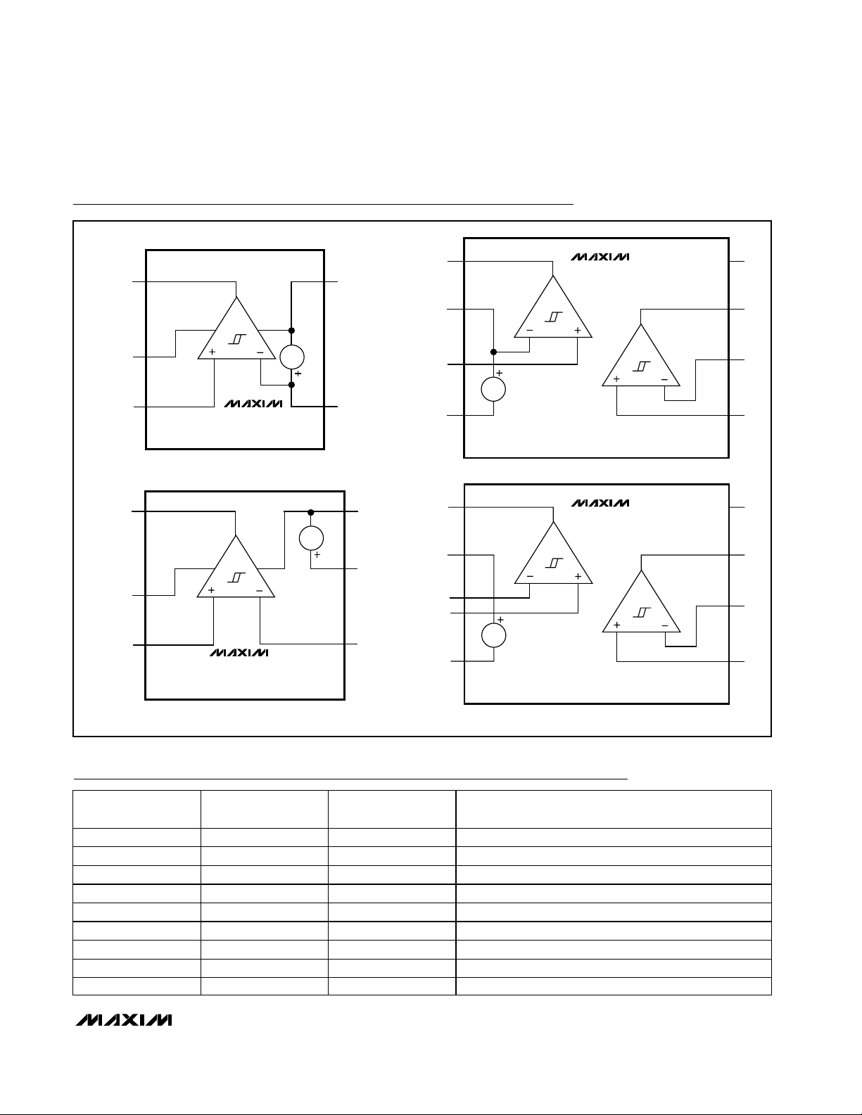
Additional Hysteresis
These comparators have ±3mV internal hysteresis.
Additional hysteresis can be generated with two resistors using positive feedback (Figure 1). Use the following procedure to calculate resistor values:
1) Calculate the trip points of the comparator using
these formulas:
and
V
TH
is the threshold voltage at which the comparator
switches its output from high to low as VINrises
above the trip point. VTLis the threshold voltage at
which the comparator switches its output from low to
high as VINdrops below the trip point.
2) The hysteresis band will be:
MAX9039–MAX9043/MAX9050–MAX9053
Micropower, Single-Supply, UCSP/SOT23
Comparator + Precision Reference ICs
_______________________________________________________________________________________ 9
Figure 1. Additional Hysteresis
V
R1
CC
VV
=+
TH REF
VVR
−
CC REF
()
12
RR
+
2
V
V
R2
REF
IN
IN+
IN-
V
CC
OUT
MAX9039–MAX9043
MAX9050–MAX9053
V
EE
VV
=−
TL REF
1
RR
2
R
12
+
VVVV
=−=
HYS TH TL CC
2
R
+
12
RR
Page 10

MAX9039–MAX9043/MAX9050–MAX9053
3) In this example, let VCC= 5V and V
REF
= 2.5V:
and
4) Select R2. In this example, we will choose 1kΩ.
5) Select V
HYS
. In this example, we will choose 50mV.
6) Solve for R1:
where R1 ≈ 100kΩ, V
TH
= 2.525V, and VTL= 2.475V.
Board Layout and Bypassing
Power-supply bypass capacitors are not typically needed, but would be called for in cases where supply
impedance is high, supply leads are long, or excessive
noise is expected on the supply lines. Use 100nF
bypass capacitors under these conditions. Minimize
signal trace lengths to reduce stray capacitance.
Reference Output/Load Capacitance
The MAX9039/MAX904_/MAX905_ do not require an
output capacitor on REF for frequency stability. They
are stable for capacitive loads up to 4.7nF. However, in
applications where the load or the supply can experience step changes, an output capacitor will reduce the
amount of overshoot (or undershoot) and assist the circuit’s transient response. When an application is not
subject to transient conditions, the REF capacitor can
be omitted.
Biasing for Data Recovery
Digital data is often embedded into a bandwidth- and
amplitude-limited analog path. Recovering the data can
be difficult. Figure 2 compares the input signal to a
time-averaged version of itself. This self-biases the
threshold to the average input voltage for optimal noise
margin.
Even severe phase distortion is eliminated from the digital output signal. Be sure to choose R1 and C1 so that:
where f
CAR
is the fundamental carrier frequency of the
digital data stream.
UCSP Package Consideration
For general UCSP package information and PC layout
considerations, please refer to Maxim Application
Note,"Wafer-Level Chip-Scale Package."
UCSP Reliability
The chip-scale package (UCSP) represents a unique
packaging form factor that may not perform equally to a
packaged product through traditional mechanical reliability tests. UCSP reliability is integrally linked to the
user’s assembly methods, circuit board material, and
usage environment. The user should closely review
these areas when considering use of a UCSP.
Performance through Operating Life Test and Moisture
Resistance remains uncompromised as it is primarily
determined by the wafer-fabrication process.
Mechanical stress performance is a greater consideration for a UCSP. UCSPs are attached through direct
solder contact to the user’s PC board, foregoing the
inherent stress relief of a packaged product lead frame.
Solder joint contact integrity must be considered.
Information on Maxim’s qualification plan, test data,
and recommendations are detailed in the UCSP application note, which can be found on Maxim’s website at
www.maxim-ic.com.
Chip Information
MAX9039 TRANSISTOR COUNT: 193
MAX9040/MAX9041/MAX9050/MAX9051 TRANSISTOR
COUNT: 204
MAX9042/MAX9043/MAX9052/MAX9053 TRANSISTOR
COUNT: 280
Micropower, Single-Supply, UCSP/SOT23
Comparator + Precision Reference ICs
10 ______________________________________________________________________________________
Figure 2. Time Averaging of the Input Signal for Data Recovery
V
CC
V
CC
25 25
=+
TH
IN+
IN-
..
RR
MAX9039–MAX9043
MAX9050–MAX9053
V
EE
2
R
12
+
OUT
V
IN
10kΩ
0.1µF
V
f
CAR
>>
2R1C1
1
π
25 1
.
V
=−
TL
2
R
12
RR
+
VV
HYS CC
0 050 5
. =
=
RR
1000
R
1 1000
2
R
+
12
+
Page 11
MAX9039–MAX9043/MAX9050–MAX9053
Micropower, Single-Supply, UCSP/SOT23
Comparator + Precision Reference ICs
______________________________________________________________________________________ 11
Functional Diagrams
Selector Guide
REF2.0481MAX9040
REF/Uncommitted
REF/Uncommitted2.500
Uncommitted/Uncommitted
2
2.5002
MAX9052
2.048
MAX9053
Uncommitted/Uncommitted
2
2.0482
MAX9042
MAX9043
REF2.500
Uncommitted
1
2.5001
MAX9050
MAX9051
Uncommitted1.230
V
REF
(V)
COMPARATORS
PER PACKAGE
Uncommitted
1
2.0481
MAX9039
MAX9041
PART IN- CONNECTIONS
OUT
1
5
V
CC
3
IN+ REF
MAX9040
MAX9050
6 (A2)
OUT
7 (A3)
V
CC
REF
REF
OUTA
1
2
V
EE
REF
2
INA+
3
4
V
4 (A1)
EE
REF
V
4
EE
1
OUTA
MAX9042
MAX9052
MAX9043
V
OUTB
INB-
INB+
V
8
CC
7
6
5
10
CC
MAX9053
REF
1 (B3)
2
REF
INA-
3
INA+
4
OUTB
INB-
8
7
3 (B1)
IN+
( ) MAX9039 UCSP BUMPS.
MAX9039
MAX9041
MAX9051
2 (B2)
IN-
REF
5
V
EE
INB+
6
Page 12

MAX9039–MAX9043/MAX9050–MAX9053
Micropower, Single-Supply, UCSP/SOT23
Comparator + Precision Reference ICs
12 ______________________________________________________________________________________
Typical Operating Circuit
Ordering Information (continued)
Pin Configurations (continued)
PINPACKAGE
8 µMAX
8 SO
8 SO
10 µMAX
10 µMAX
5 SOT23-5
5 SOT23-5
6 SOT23-6
6 SOT23-6
8 SO
8 µMAX-40°C to +85°CMAX9042BEUA —
-40°C to +85°C
-40°C to +85°C
-40°C to +85°C
-40°C to +85°C
-40°C to +85°C
-40°C to +85°C
-40°C to +85°C
-40°C to +85°C
-40°C to +85°C
-40°C to +85°C
TEMP RANGEPART
MAX9042AEUA
MAX9042AESA
MAX9042BESA
MAX9043AEUB
MAX9043BEUB
MAX9050AEUK-T
MAX9050BEUK-T
MAX9051AEUT-T
MAX9051BEUT-T
MAX9051AESA
TOP
MARK
—
—
—
—
—
ADNW
ADNY
AAHG
AAHI
—
8 SO-40°C to +85°CMAX9051BESA —
8 µMAX
8 µMAX
8 SO-40°C to +85°C
-40°C to +85°C
-40°C to +85°C
MAX9052AEUA
MAX9052BEUA
MAX9052AESA
8 SO-40°C to +85°C
AAHG
AAHI
—
MAX9052BESA —
10 µMAX-40°C to +85°CMAX9053BEUB —
10 µMAX-40°C to +85°C
MAX9053AEUA
—
TOP VIEW
OUT
16V
V
MAX9041
2
EE
MAX9051
34
5 REF
IN-IN+
CC
REF
IN-
IN+
1
2
MAX9041
MAX9051
3
4
EE
87N.C.
6
5
V
OUT
N.C.V
OUTA
1
INA+
2
MAX9042
MAX9052
3
4
EE
CC
V
OUTA
REF
INA-
1
2
MAX9043
3
MAX9053
4
5
EE
8
CC
OUTBREF
7
INB-
6
INB+V
5
V
10
CC
9
N.C.
8
OUTB
7
INB-INA+
6
INB+V
SOT23
SO
µMAX/SO
V
IN
1.23V/2.048V/2.500V
V
CC
V
CC
IN+
IN-
REF
V
EE
MAX9039
MAX9041/MAX9043
MAX9051/MAX9053
µMAX
0.1µF
OUT
Page 13

MAX9039–MAX9043/MAX9050–MAX9053
Micropower, Single-Supply, UCSP/SOT23
Comparator + Precision Reference ICs
______________________________________________________________________________________ 13
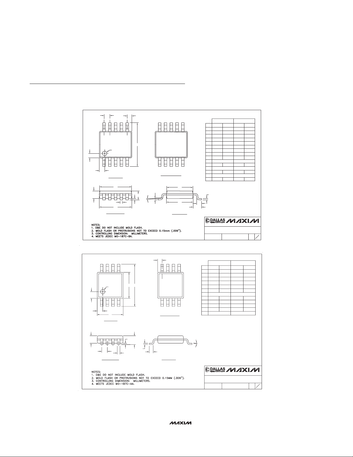
Package Information
(The package drawing(s) in this data sheet may not reflect the most current specifications. For the latest package outline information,
go to www.maxim-ic.com/packages.)
6L, UCSP.EPS
SOT5L.EPS
Page 14

MAX9039–MAX9043/MAX9050–MAX9053
Micropower, Single-Supply, UCSP/SOT23
Comparator + Precision Reference ICs
14 ______________________________________________________________________________________
Package Information (continued)
(The package drawing(s) in this data sheet may not reflect the most current specifications. For the latest package outline information,
go to www.maxim-ic.com/packages.)
N
1
e
TOP VIEW
D
FRONT VIEW
INCHES
DIM
MIN
0.053A
0.004
A1
0.014
B
0.007
C
e 0.050 BSC 1.27 BSC
0.150
HE
A
B
A1
C
L
SIDE VIEW
E
H 0.2440.228 5.80 6.20
0.016L
VARIATIONS:
INCHES
MINDIM
D
0.189 0.197 AA5.004.80 8
0.337 0.344 AB8.758.55 14
D
0∞-8∞
PROPRIETARY INFORMATION
TITLE:
PACKAGE OUTLINE, .150" SOIC
MAX
0.069
0.010
0.019
0.010
0.157
0.050
MAX
0.3940.386D
MILLIMETERS
MAX
MIN
1.35
1.75
0.10
0.25
0.35
0.49
0.19
0.25
3.80 4.00
0.40 1.27
MILLIMETERS
MAX
MIN
9.80 10.00
21-0041
N MS012
16
REV.DOCUMENT CONTROL NO.APPROVAL
SOICN .EPS
AC
1
B
1
6LSOT.EPS
Page 15
Micropower, Single-Supply, UCSP/SOT23
Comparator + Precision Reference ICs
MAX9039–MAX9043/MAX9050–MAX9053
Maxim cannot assume responsibility for use of any circuitry other than circuitry entirely embodied in a Maxim product. No circuit patent licenses are
implied. Maxim reserves the right to change the circuitry and specifications without notice at any time.
Maxim Integrated Products, 120 San Gabriel Drive, Sunnyvale, CA 94086 408-737-7600 ____________________ 15
© 2002 Maxim Integrated Products Printed USA is a registered trademark of Maxim Integrated Products.
Package Information (continued)
(The package drawing(s) in this data sheet may not reflect the most current specifications. For the latest package outline information,
go to www.maxim-ic.com/packages.)
0.6±0.1
e
10
ÿ 0.50±0.1
1
0.6±0.1
TOP VIEW
D2
A2
D1
FRONT VIEW
4X S
H
BOTTOM VIEW
GAGE PLANE
A
b
α
A1
10
1
E2
E1
L
L1
INCHES
MILLIMETERS
MAX
0.043
0.006
0.120
0.118
0.120
0.118
0.199
0.0275
0.0106
0.0078
MIN
-
0.05
2.95
2.89
2.95
2.89
4.75
0.40
0.940 REF
0.177
0.500 BSC
0.090
0.498 REF
6∞
MIN
DIM
-A
A1
0.002
A2 0.030 0.037 0.75 0.95
D1
0.116
0.114
D2
0.116
E1
0.114
E2
0.187
H
0.0157
L
L1
0.037 REF
0.007
b
e
0.0197 BSC
0.0035
c
0.0196 REF
S
α
0∞ 0∞ 6∞
c
MAX
1.10
0.15
3.05
3.00
3.05
3.00
5.05
0.70
0.270
0.200
10LUMAX.EPS
SIDE VIEW
PROPRIETARY INFORMATION
TITLE:
PACKAGE OUTLINE, 10L uMAX/uSOP
21-0061
REV.DOCUMENT CONTROL NO.APPROVAL
1
I
1
0.6±0.1
0.6±0.1
8
ÿ 0.50±0.1
1
D
E H
4X S
BOTTOM VIEW
8
1
DIM
A
A1
A2
b
c
D
e
E
H
L
α
S
INCHES
MIN
-
0.002
0.030
0.010
0.005
0.116
0.0256 BSC
0.116
0.188
0.016
0∞
0.0207 BSC
MAX
0.043
0.006
0.037
0.014
0.007
0.120
0.120
0.198
0.026
6∞
MILLIMETERS
MIN
- 1.10
0.05 0.15
0.25 0.36
0.13 0.18
2.95 3.05
0.65 BSC
2.95 3.05
4.78
0.41
0.5250 BSC
MAX
0.950.75
5.03
0.66
8LUMAXD.EPS
6∞0∞
TOP VIEW
A2
e
FRONT VIEW
A1
A
c
b
L
α
SIDE VIEW
PROPRIETARY INFORMATION
TITLE:
PACKAGE OUTLINE, 8L uMAX/uSOP
21-0036
REV.DOCUMENT CONTROL NO.APPROVAL
1
J
1
 Loading...