

Page 1
General Description
The MAX900–MAX903 high-speed, low-power, single/
dual/quad voltage comparators feature differential analog inputs and TTL-logic outputs with active internal pullups. Fast propagation delay (8ns typ at 5mV overdrive)
makes the MAX900–MAX903 ideal for fast A/D converters and sampling circuits, line receivers, V/F converters,
and many other data-discrimination applications.
All comparators can be powered from separate analog
and digital power supplies or from a single combined supply voltage. The analog input common-mode range
includes the negative rail, allowing ground sensing when
powered from a single supply. The MAX900–MAX903
consume 18mW per comparator when powered from +5V.
The MAX900–MAX903 are equipped with independent
TTL-compatible latch inputs. The comparator output
states are held when the latch inputs are driven low. The
MAX901 provides the same performance as the
MAX900/MAX902/MAX903 with the exception of the
latches.
For newer, pin-for-pin compatible parts with the same
speed and only half the power dissipation, see the
MAX9201/MAX9202/MAX9203 data sheet.
Applications
Features
♦ 8ns (typ) Propagation Delay
♦ 18mW/Comparator Power Consumption (+5V, typ)
♦ Separate Analog and Digital Supplies
♦ Flexible Analog Supply: +5V to +10V or ±5V
♦ Input Range Includes Negative Supply Rail
♦ TTL-Compatible Outputs
♦ TTL-Compatible Latch Inputs (Except MAX901)
MAX900–MAX903
High-Speed, Low-Power Voltage Comparators
________________________________________________________________ Maxim Integrated Products 1
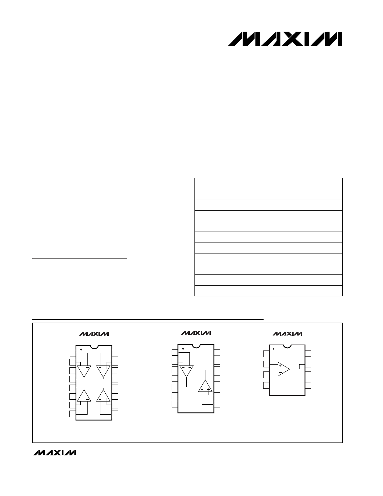
Pin Configurations
Ordering Information
19-2887; Rev. 4; 7/01
For pricing, delivery, and ordering information, please contact Maxim/Dallas Direct! at
1-888-629-4642, or visit Maxim’s website at www.maxim-ic.com.
Ordering Information continued at end of data sheet.
Pin Configurations continued at end of data sheet.
High-Speed A/D
Converters
High-Speed V/F
Converters
Line Receivers
Threshold Detectors
Input Trigger Circuitry
High-Speed Data
Sampling
PWM Circuits
PART TEMP RANGE PIN-PACKAGE
MAX900ACPP 0°C to +70°C 20 Plastic DIP
MAX900BCPP 0°C to +70°C 20 Plastic DIP
MAX900ACWP 0°C to +70°C 20 Wide SO
MAX900BCWP 0°C to +70°C 20 Wide SO
MAX900AEPP -40°C to +85°C 20 Plastic DIP
MAX900BEPP -40°C to +85°C 20 Plastic DIP
MAX900AEWP -40°C to +85°C 20 Wide SO
MAX900BEWP -40°C to +85°C 20 Wide SO
MAX901ACPE 0°C to +70°C 16 Plastic DIP
MAX901BCPE 0°C to +70°C 16 Plastic DIP
TOP VIEW
MAX901
1
IN- (A) IN- (D)
IN+ (A)
2
GND
3
AD
4
OUT (A)
OUT (B)
5
BC
*
V
6
EE
IN+ (B)
7
IN- (B)
8
DIP/SO
16
15
14
13
12
11
10
9
IN+ (D)
**
V
CC
OUT (D)
OUT (C)
**
V
DD
IN+ (C)
IN- (C)
IN- (A)
IN+ (A)
GND
OUT (A)
N.C.
MAX902
1
2
3
4
A
5
6
*
7
EE
DIP/SO
14
VCC**
13
N.C.
12
OUT (B)
B
11
LATCH (B)LATCH (A)
10
VDD***
9
IN+ (B)
IN- (B)V
8
MAX903
1
VCC**
2
IN-
3
4
*
EE
DIP/SO
*ANALOG V- AND SUBSTRATE
**ANALOG V+
***DIGITAL V+
87VDD***
6
5
OUTIN+
GND
LATCHV
Page 2
MAX900–MAX903
High-Speed, Low-Power Voltage Comparators
2 _______________________________________________________________________________________
ABSOLUTE MAXIMUM RATINGS
ELECTRICAL CHARACTERISTICS
(VCC= +5V, VEE= -5V, VDD= +5V, LE1–LE4 = logic high, TA= +25°C, unless otherwise noted.)
Stresses beyond those listed under “Absolute Maximum Ratings” may cause permanent damage to the device. These are stress ratings only, and functional
operation of the device at these or any other conditions beyond those indicated in the operational sections of the specifications is not implied. Exposure to
absolute maximum rating conditions for extended periods may affect device reliability.
Analog Supply Voltage (VCCto VEE) ...................................+12V
Digital Supply Voltage (VDDto GND) ....................................+7V
Differential Input Voltage..................(V
EE
- 0.2V) to (VCC+ 0.2V)
Common-Mode Input Voltage..........(V
EE
- 0.2V) to (VCC+ 0.2V)
Latch-Input Voltage (MAX900/MAX902/
MAX903 only) .........................................-0.2V to (V
DD
+ 0.2V)
Output Short-Circuit Duration
To GND.......................................................................Indefinite
To V
DD
...............................................................................1min
Internal Power Dissipation................................................500mW
Derate above +100°C ................................................10mW/°C
Operating Temperature Ranges:
MAX900–MAX903_C_ _ .......................................0°C to +70°C
MAX900–MAX903_E_ _ ....................................-40°C to +85°C
Junction Temperature........................................-65°C to +160°C
Storage Temperature Range .............................-65°C to +150°C
Lead Temperature (soldering, 10s) .................................+300°C
PARAMETER SYMBOL CONDITIONS
Input Offset Voltage V
Input Bias Current I
Input Offset Current I
Input Voltage Range V
OS
B
OS
CM
VCM = 0
V
= 1.4V
O
IIN+ or IIN- 3 6 4 10 µA
VCM = 0;
V
= 1.4V
O
(Note 1) VEE - 0.1
MAX900A/MAX901A
MIN TYP MAX MIN TYP MAX
0.5 2.0 1.0 4.0 mV
50 250 100 500 nA
V
-
CC
2.25
MAX900B/MAX901B/
MAX902/MAX903
V
- 0.1
EE
V
CC
2.25
-
UNITS
V
Common-Mode Rejection
Ratio
Power-Supply Rejection
Ratio
Output High Voltage V
Output Low Voltage V
Latch-Input Voltage High V
Latch-Input Voltage Low V
Latch-Input Current High I
Latch-Input Current Low I
CMRR
PSRR (Note 2) 50 150 100 250 µV/V
LH
OH
OL
LH
LL
LL
-5V < V
+2.75V,
V
O
(Note 2)
VIN > 250mV,
I
SRC
VIN > 250mV,
I
SINK
(Note 3) 1.4 2.0 1.4 2.0 V
(Note 3) 0.8 1.4 0.8 1.4 V
VLH = 3.0V
(Note 3)
VLL = 0.3V
(Note 3)
CM
= 1.4V
= 1mA
= 8mA
<
50 150 75 250 µV/V
2.4 3.5 2.4 3.5 V
0.3 0.4 0.3 0.4 V
1 20 1 20 µA
1 20 1 20 µA
Page 3

MAX900–MAX903
High-Speed, Low-Power Voltage Comparators
_______________________________________________________________________________________ 3
ELECTRICAL CHARACTERISTICS (continued)
(VCC= +5V, VEE= -5V, VDD= +5V, LE1–LE4 = logic high, TA= +25°C, unless otherwise noted.)
TIMING CHARACTERISTICS
(VCC= +5V, VEE= -5V, VDD= +5V, LE1–LE4 = logic high, TA= +25°C, unless otherwise noted.)
PARAMETER SYMBOL CONDITIONS
Positive Analog
Supply Current
Negative Analog
Supply Current
Digital Supply
Current
Power
Dissipation
I
I
I
PD
(Note 7) 10 15 5 8 2.5 4 mA
CC
(Note 7) 7 12 3.5 6 2 3 mA
EE
(Note 7) 4 6 2 3 1 1.5 mA
DD
V
= VDD =
CC
+5V, V
EE
= 0
M AX900A/M AX901A
M AX900B/M AX901B
MIN TYP MAX MIN TYP MAX MIN TYP MAX
70 105 35 55 18 28 mW
MAX902 MAX903
PARAMETER SYMBOL CONDITIONS
VOD = 5mV,
= 15pF,
Input-to-Output High
Response Time
Input-to-Output Low
Response Time
Difference in
Response Time
Between Outputs
t
pd+
t
∆t
pd
C
L
I
= 2mA
O
(Note 4)
= 5mV,
V
OD
= 15pF,
C
L
I
= 2mA
O
(Note 4)
(Notes 4, 5) 0.5 2.0 0.5 2.0 0.5 2.0 ns
pd
MAX900A/MAX901A
MAX900B/MAX901B
MIN TYP MAX MIN TYP MAX MIN TYP MAX
810 810 810 ns
810 810 810 ns
MAX902 MAX903
UNITS
UNITS
Latch Disable to
Output High Delay
Latch Disable to
Output Low Delay
Minimum Setup Time t
Minimum Hold Time t
Minimum Latch
Disable Pulse Width
t
pd+ (D)
t
pd- (D)
t
pw (D)
(Notes 3, 6) 10 10 10 ns
(Notes 3, 6) 12 12 12 ns
(Notes 3, 6) 2 2 2 ns
s
(Notes 3, 6) 1 1 1 ns
h
(Notes 3, 6) 10 10 10 ns
Page 4
MAX900–MAX903
High-Speed, Low-Power Voltage Comparators
4 _______________________________________________________________________________________
ELECTRICAL CHARACTERISTICS
(VCC= +5V, VEE= -5V, VDD= +5V, LE1–LE4 = logic high, TA= full operating temperature, unless otherwise noted.)
PARAMETER SYMBOL CONDITIONS
Input Offset Voltage V
OS
VCM = 0,
V
= 1.4V
O
MAX900A/MAX901A
MIN TYP MAX MIN TYP MAX
13 26 mV
MAX900B/MAX901B/
MAX902/MAX903
UNITS
Input Bias Current I
Input Offset Current I
Input Voltage Range V
Common-Mode
Rejection Ratio
Power-Supply
Rejection Ratio
Output High Voltage V
Output Low Voltage V
Latch Input Voltage
High
Latch Input Voltage
Low
Latch Input Current
High
Latch Input Current
Low
B
OS
CM
CMRR
PSRR (Note 2) 100 250 150 500 µV/V
OH
OL
V
LH
V
LL
I
LH
I
LL
I
IN+
VCM = 0,
= 1.4V
V
O
(Note 1)
-5V < V
+2.75V,
V
= 1.4V
O
(Note 2)
VIN > 250mV,
I
SRC
VIN > 250mV,
I
SINK
(Note 7) 1.4 2.0 1.4 2.0 V
(Note 7) 0.8 1.4 0.8 1.4 V
VLH = 3.0V
(Note 7)
VLL = 0.3V
(Note 7)
or I
IN-
CM
= 1mA
= 8mA
4 10 6 15 µA
100 500 200 800 nA
V
-
EE
0.1
<
80 250 120 500 µV/V
2.4 3.5 2.4 3.5 V
0.3 0.4 0.3 0.4 V
2 20 1 20 µA
2 20 1 20 µA
VCC -
2.25
VEE -
0.1
VCC -
2.25
V
Page 5

MAX900–MAX903
High-Speed, Low-Power Voltage Comparators
_______________________________________________________________________________________ 5
ELECTRICAL CHARACTERISTICS (continued)
(VCC= +5V, VEE= -5V, VDD= +5V, LE1–LE4 = logic high, TA= full operating temperature, unless otherwise noted.)
TIMING CHARACTERISTICS
(VCC= +5V, VEE= -5V, VDD= +5V, LE1–LE4 = logic high, TA= full operating temperature, unless otherwise noted.)
Note 1: The input common-mode voltage and input signal voltages should not be allowed to go negative by more than 0.2V below
V
EE
. The upper-end of the common-mode voltage range is typically VCC- 2V, but either or both inputs can go to a maximum
of VCC+ 0.2V without damage.
Note 2: Tested for +4.75V < V
CC
< +5.25V, and -5.25V < V
EE
< -4.75V with VDD= +5V, although permissible analog power-supply
range is +4.75V < V
CC
< +10.5V for single-supply operation with VEEgrounded.
Note 3: Specification does not apply to MAX901.
Note 4: Guaranteed by design. Times are for 100mV step inputs (see Propagation Delay Characteristics in Figures 2 and 3).
Note 5: Maximum difference in propagation delay between any of the four comparators in the MAX900–MAX903.
Note 6: See Timing Diagram (Figure 2). Owing to the difficult and critical nature of switching measurements involving the latch,
these parameters cannot be tested in a production environment. Typical specifications listed are taken from measurements
using a high-speed test-jig.
Note 7: I
CC
tested for +4.75V < VCC< +10.5V with VEEgrounded. IEEtested for -5.25V < VEE< -4.75V with VCC= +5V. IDDtested
for +4.75V < V
DD
< +5.25V with the worst-case condition of all four comparator outputs at logic low.
PARAMETER SYMBOL CONDITIONS
Positive Analog
Supply Current
Negative Analog
Supply Current
Digital Supply
Current
Power
Dissipation
I
CC
I
EE
I
DD
P
(Note 7) 10 25 5 12 2.5 6 mA
(Note 7) 7 20 3.5 10 2 5 mA
(Note 7) 4 10 2 5 1 2.5 mA
VCC = VDD =
D
+5V, V
EE
= 0
MAX900A/MAX901A/
MAX900B/MAX901B
MIN TYP MAX MIN TYP MAX MIN TYP MAX
70 105 35 55 18 28 mW
MAX902 MAX903
PARAMETER SYMBOL CONDITIONS
Input-to-Output High
Response Time
t
pd+
VOD = 5mV,
C
= 15pF,
L
= 2mA
I
O
(Note 4)
MAX900A/MAX901A
MIN TYP MAX MIN TYP MAX
10 15 10 15 ns
MAX900B/MAX901B/
MAX902/MAX903
UNITS
UNITS
VOD = 5mV,
Input-to-Output Low
Response Time
Difference in Response
Time Between Outputs
t
pd-
∆t
pd
C
= 15pF,
L
= 2mA
I
O
(Note 4)
(Notes 4, 5) 1 3 1 3 ns
10 15 10 15 ns
Page 6

MAX900–MAX903
High-Speed, Low-Power Voltage Comparators
Typical Operating Characteristics
(TA = +25°C, unless otherwise noted.)
0
-1
-2
1
2
200-40 -20 40 60 80 100 120
INPUT OFFSET VOLTAGE
vs. TEMPERATURE
MAX900-03 toc01
TEMPERATURE (°C)
INPUT OFFSET VOLTAGE (mV)
3.0
2.5
2.0
3.5
4.0
200-40 -20 40 60 80 100 120
INPUT BIAS CURRENT
vs. TEMPERATURE
MAX900-03 toc02
TEMPERATURE (°C)
INPUT BIAS VOLTAGE (µV)
0.2
0.1
0.4
0.3
0.5
OUTPUT LOW VOLTAGE
(V
OL
) vs. LOAD CURRENT
MAX900-03 toc03
LOAD CURRENT (mA)
OUTPUT LOW VOLTAGE (V)
462810
TA = -55°C
TA = +125°C
TA = +25°C
1.8
1.6
2.4
2.2
2.0
3.0
2.8
2.6
6745 8910
ICC SUPPLY CURRENT (PER COMPARATOR)
vs. V
CC
SUPPLY VOLTAGE
MAX900-03 toc04
VCC SUPPLY VOLTAGE (V)
I
CC
SUPPLY CURRENT (mA)
TA = +125°C
TA = +25°C
TA = -55°C
VDD = +5V
0
-100
1
0
100
3
4
2
460 2 8 101214
IINPUT OVERDRIVE vs.
t
pd+
RESPONSE TIME
MAX900-03 toc05
tpd+ RESPONSE TIME (ns)
INPUT VOLTAGE OUTPUT VOLTAGE
INPUT OVERDRIVE (VOD)
25mV
2mV
5mV
0
-100
1
0
100
3
4
2
460 2 8 101214
INPUT OVERDRIVE vs.
t
pd-
RESPONSE TIME
MAX900-03 toc06
tpd- RESPONSE TIME (ns)
INPUT VOLTAGE OUTPUT VOLTAGE
INPUT OVERDRIVE (VOD)
25mV
2mV
5mV
5
7
6
9
8
10
11
13
12
14
-40 -20 0 20 40 60 80 100 120
RESPONSE TIME vs.
TEMPERATURE (5mV OVERDRIVE)
MAX900-03 toc07
TEMPERATURE (°C)
RESPONSE TIME (ns)
t
pd+
t
pd-
8
7
10
9
11
12
14
13
10 20 30 40 50 60 70 80
RESPONSE TIME vs. LOAD CAPACITANCE
(5mV OVERDRIVE)
MAX900-03 toc08
LOAD CAPACITANCE (pF)
t
pd-
t
pd+
RL = 2.4kΩ
6 ____________________________________________________________________________________________________
Page 7

MAX900–MAX903
High-Speed, Low-Power Voltage Comparators
_______________________________________________________________________________________ 7
Pin Descriptions
MAX900
MAX901
MAX902
MAX903
PIN NAME FUNCTION
1, 10, 11, 20 IN- (A, B, C, D)
2, 9, 12, 19 IN+ (A, B, C, D)
3 GND Ground Terminal
4, 7, 14, 17
5, 6, 15, 16 OUT (A, B, C, D)
8V
13 V
18 V
PIN NAME FUNCTION
1, 8 IN- (A, B)
2, 9 IN+ (A, B)
3 GND Ground Terminal
4, 11 LATCH (A, B)
5, 12 OUT (A, B) Output (Channels A, B)
6, 13 N.C.
7V
10 V
14 V
LATCH (A, B, C,D)Latch Input (Channels
EE
DD
CC
EE
DD
CC
Negative Input
(Channels A, B, C, D)
Positive Input
(Channels A, B, C, D)
A, B, C, D)
Output (Channels A, B,
C, D)
Negative Analog
Supply and Substrate
Positive Digital Supply
Positive Analog Supply
Negative Input
(Channels A, B)
Positive Input
(Channels A, B)
Latch Input (Channels
A, B)
No Connection. Not
internally connected.
Negative Analog
Supply and Substrate
Positive Digital Supply
Positive Analog Supply
PIN NAME FUNCTION
1, 8, 9, 16 IN- (A, B, C, D)
2, 7, 10, 15 IN+ (A, B, C, D)
3 GND Ground Terminal
4, 5, 12, 13 OUT (A, B, C, D)
6V
11 V
14 V
EE
DD
CC
Negative Input
(Channels A, B, C, D)
Positive Input
(Channels A, B, C, D)
Output (Channels A,
B, C, D)
Negative Analog
Supply and Substrate
Positive Digital Supply
Positive Analog
Supply
PIN NAME FUNCTION
1VCCPositive Analog Supply
2 IN+ Positive Input
3 IN- Negative Input
4V
5 LATCH Latch Input
6 GND Ground Terminal
7 OUT Output
8VDDPositive Digital Supply
EE
Negative Analog
Supply and Substrate
Page 8

MAX900–MAX903
High-Speed, Low-Power Voltage Comparators
8 _______________________________________________________________________________________
Applications Information
Circuit Layout
Because of the large gain-bandwidth transfer function of
the MAX900–MAX903, special precautions must be
taken to realize their full high-speed capability. A printed
circuit board with a good, low-inductance ground plane
is mandatory. All decoupling capacitors (the small
100nF ceramic type is a good choice) should be mounted as close as possible to the power-supply pins.
Separate decoupling capacitors for analog VCCand for
digital VDDare also recommended. Close attention
should be paid to the bandwidth of the decoupling and
terminating components. Short lead lengths on the
inputs and outputs are essential to avoid unwanted parasitic feedback around the comparators. Solder the
device directly to the printed circuit board instead of
using a socket.
Input Slew-Rate Requirements
As with all high-speed comparators, the high gain-bandwidth product of the MAX900–MAX903 can create oscillation problems when the input traverses the linear
region. For clean output switching without oscillation or
steps in the output waveform, the input must meet minimum slew-rate requirements. Oscillation is largely a
function of board layout and of coupled source impedance and stray input capacitance. Both poor layout and
large-source impedance will cause the part to oscillate
and increase the minimum slew-rate requirement. In
some applications, it may be helpful to apply some positive feedback between the output and + input. This
pushes the output through the transition region cleanly,
but applies a hysteresis in threshold seen at the input
terminals.
TTL Output and Latch Inputs
The comparator TTL-output stages are optimized for driving low-power Schottky TTL with a fan-out of four.
When the latch is connected to a logic high level or left
floating, the comparator is transparent and immediately
responds to changes at the input terminals. When the
latch is connected to a TTL low level, the comparator
output latches in the same state as at the instant that the
latch command is applied, and will not respond to subsequent changes at the input. No latch is provided on
the MAX901.
Power Supplies
The MAX900–MAX903 can be powered from separate
analog and digital supplies or from a single +5V supply.
The analog supply can range from +5V to +10V with
VEEgrounded for single-supply operation (Figures 1A
and 1B) or from a split ±5V supply (Figure 1C). The V
DD
digital supply always requires +5V.
In high-speed, mixed-signal applications where a common ground is shared, a noisy digital environment can
adversely affect the analog input signal. When set up
with separate supplies (Figure 1C), the
MAX900–MAX903 isolate analog and digital signals by
providing a separate AGND (VEE) and DGND.
Figure 1A. Separate Analog Supply,
Common Ground
Figure 1B. Single +5V Supply, Common
Ground
Figure 1C. Split ±5V Supply, Separate
Ground
Typical Power-Supply Alternatives
+10V
+5V
V
CC
V
DD
GND
V
EE
OUT
+5V
V
CC
V
DD
GND
V
EE
OUT
+5V
-5V
V
CC
V
EE
+5V
V
DD
GND
OUT
Page 9

MAX900–MAX903
High-Speed, Low-Power Voltage Comparators
_______________________________________________________________________________________ 9
Definitions of Terms
V
V
V
t
pd+
OS
IN
OD
Input Offset Voltage: Voltage applied
between the two input terminals to obtain
TTL-logic threshold (+1.4V) at the
output.
Input Voltage Pulse Amplitude: Usually
set to 100mV for comparator
specifications.
Input Voltage Overdrive: Usually set to
5mV and in opposite polarity to V
comparator specifications.
Input-to-Output High Delay: The
propagation delay measured from the
time the input signal crosses the input
offset voltage to the TTL-logic threshold
of an output low-to-high transition
IN
for
t
pd+ (D)
t
pd- (D)
t
s
t
h
Latch Disable-to-Output High Delay:
The propagation delay measured from
the latch-signal crossing the TTL
threshold in a low-to-high transition to
the point of the output crossing TTL
threshold in a low-to-high transition.
Latch Disable-to-Output Low Delay:
The propagation delay measured from
the latch-signal crossing the TTL
threshold in a low-to-high transition to
the point of the output crossing TTL
threshold in a high-to-low transition.
Minimum Setup Time: The minimum
time before the negative transition of the
latch signal that an input signal change
must be present in order to be acquired
and held at the outputs.
Minimum Hold Time: The minimum time
after the negative transition of the latch
signal that an input signal must remain
unchanged in order to be acquired and
held at the output.
t
pd-
Input-to-Output Low Delay: The
propagation delay measured from the
time the input signal crosses the input
offset voltage to the TTL-logic threshold
of an output high-to-low transition.
tpw (D) Minimum Latch-Disable Pulse Width:
The minimum time that the latch signal
must remain high in order to acquire and
hold an input-signal change.
Page 10

MAX900–MAX903
High-Speed, Low-Power Voltage Comparators
10 ______________________________________________________________________________________
Figure 2. MAX900/MAX902/MAX903 Timing Diagram
Figure 4. t
pd-
Response Time to 5mV Overdrive
Figure 5. Response-Time Setup
Figure 3. t
pd+
Response Time to 5mV Overdrive
LATCH
ENABLE
INPUT
LATCH LATCH LATCH
DIFFERENTAL
INPUT VOLTAGE
COMPARATOR
OUTPUT
COMPARE COMPARE
t
t
s
h
V
IN
V
DD
t
pd-
OUTPUT
INPUT
5ns/div
tpw(D)
1.4V
OUTPUT
V
OS
INPUT
1kΩ
5ns/div
100nF
10Ω
10Ω
V
V
CC
D.U.T.
EE
+5V
100nF
-5V
t
(D)
pd+
+5V
0
100mV
1.4V
V
OS
+5mV
PRECISION
STEP GENERATOR
INPUT TO 10X
SCOPE PROBE
(10MΩ, 14pF)
V
DC
OFFSET
ADJUST
10kΩ
100nF
+5V
0
V
+5mV
100mV
+5V
V
DD
R
L
2.43kΩ
OUTPUT TO 10X
SCOPE PROBE
(10MΩ, 14pF)
100nF
OS
Page 11

MAX900–MAX903
High-Speed, Low-Power Voltage Comparators
______________________________________________________________________________________ 11
Figure 6. Response to 50MHz Sine Wave
Figure 8. Alarm Circuit Level Monitors Eight Separate Inputs
Figure 7. Response to 100MHz Sine Wave Photo
Typical Application
Programmed, Variable-Alarm Limits
By combining two quad analog comparators with an
octal 8-bit D/A converter (the MX7228), several alarm
and limit-defect functions can be performed simultaneously without external adjustments
The MX7228’s internal latches allow the system
processor to set the limit points for each comparator
independently and update them at any time. Set the
upper and lower thresholds for a single transducer by
pairing the D/A converter and comparator sections.
OUTPUT
1V/div
OUTPUT
1V/div
INPUT
10mV/div
5ns/div
+1.25V
VREF
MSB
8-BIT
DATA
INPUT
MX7228
VDAC1
OCTAL
8-BIT
DAC
D7
8 x 8
DATA
LATCH
LSB
D1
V
OUT1
IN2
IN3
IN6
INPUT
10mV/div
5ns/div
IN1
UNDER
LIMIT
OVER
LIMIT
UNDER
LIMIT
IN4
MAX901
IN5
UNDER
LIMIT
UNDER
LIMIT
UNDER
LIMIT
OVER
IN7
A0
CONTROL
A1
A2
LOGIC
VDAC8
V
OUT8
IN8
MAX901
LIMIT
OVER
LIMIT
Page 12

MAX900–MAX903
High-Speed, Low-Power Voltage Comparators
Maxim cannot assume responsibility for use of any circuitry other than circuitry entirely embodied in a Maxim product. No circuit patent licenses are
implied. Maxim reserves the right to change the circuitry and specifications without notice at any time.
12 ____________________Maxim Integrated Products, 120 San Gabriel Drive, Sunnyvale, CA 94086 408-737-7600
© 2001 Maxim Integrated Products Printed USA is a registered trademark of Maxim Integrated Products.
Ordering Information (continued) Pin Configurations (continued)
PART TEMP RANGE PIN-PACKAGE
MAX901ACSE 0°C to +70°C 16 Narrow SO
MAX901BCSE 0°C to +70°C 16 Narrow SO
MAX901AEPE -40°C to +85°C 16 Plastic DIP
MAX901BEPE -40°C to +85°C 16 Plastic DIP
MAX901AESE -40°C to +85°C 16 Narrow SO
MAX901BESE -40°C to +85°C 16 Narrow SO
MAX902CPD 0°C to +70°C 14 Plastic DIP
MAX902CSD 0°C to +70°C 14 Narrow SO
MAX902EPD -40°C to +85°C 14 Plastic DIP
MAX902ESD -40°C to +85°C 14 Narrow SO
MAX903CPA 0°C to +70°C 8 Plastic DIP
MAX903CSA 0°C to +70°C 8 SO
MAX903EPA -40°C to +85°C 8 Plastic DIP
TOP VIEW
IN- (A)
IN+ (A)
GND
OUT (A)
OUT (B)
LATCH (B)
IN+ (B)
1
2
3
AD
4
5
MAX900
6
7
BC
8
9
10
DIP/SO
20
IN- (D)
19
IN+ (D)
**
18
V
CC
LATCH (D)LATCH (A)
17
16
OUT (D)
15
OUT (C)
14
LATCH (C)
***VEE*
13
V
DD
12
IN+ (C)
11
IN- (C)IN- (B)
*ANALOG V- AND SUBSTRATE
**ANALOG V+
***DIGITAL V+
MAX903ESA -40°C to +85°C 8 SO
 Loading...