

Page 1
General Description
The MAX9010/MAX9011/MAX9013 single and MAX9012
dual, high-speed comparators operate from a single
4.5V to 5.5V power supply and feature low-current consumption. They have precision differential inputs and
TTL outputs. They feature short propagation delay (5ns,
typ), low-supply current, and a wide common-mode
input range that includes ground. They are ideal for lowpower, high-speed, single-supply applications.
The comparator outputs remain stable through the linear
region when driven with slow-moving or low input-overdrive signals, eliminating the output instability common
to other high-speed comparators. The input voltage
range extends to 200mV below ground with no output
phase reversal. The MAX9013 features complementary
outputs and both the MAX9011/MAX9013 have a latch
enable input (LE). The MAX9013 is an improved plug-in
replacement for the industry-standard MAX913 and
LT1016/LT1116, offering lower power and higher speed
when used in a single 5V supply application.
For space-critical designs, the single MAX9010 is available in the tiny 6-pin SC70 package. The single
MAX9011 is available in a space-saving 6-pin SOT23
package. The dual MAX9012 and the single MAX9013
are available in 8-pin µMAX and 8-pin SO packages. All
products in the family are guaranteed over the extended
temperature range of -40°C to +85°C.
Applications
High-Speed Signal Squaring
Zero-Crossing Detectors
High-Speed Line Receivers
High-Speed Sampling Circuits
High-Speed Triggers
Fast Pulse-Width/Height Discriminators
____________________________Features
♦ Ultra-Fast, 5ns Propagation Delay
♦ Low Quiescent Current:
900µA (MAX9010/MAX9011)
1.3mA (MAX9013)
2.4mA (MAX9012)
♦ Single-Supply 4.5V to 5.5V Applications
♦ Input Range Extends Below Ground
♦ No Minimum Input Signal Slew-Rate Requirement
♦ No Supply-Current Spikes During Switching
♦ Stable when Driven with Slow-Moving Inputs
♦ No Output Phase Reversal for Overdriven Inputs
♦ TTL-Compatible Outputs (Complementary for
MAX9013)
♦ Latch Function Included (MAX9011/MAX9013)
♦ High-Precision Comparators
0.7mV Input Offset Voltage
3.0V/mV Voltage Gain
♦ Available in Tiny 6-Pin SC70 and SOT23 Packages
MAX9010–MAX9013
SC70, 5ns, Low-Power, Single-Supply,
Precision TTL Comparators
________________________________________________________________ Maxim Integrated Products 1
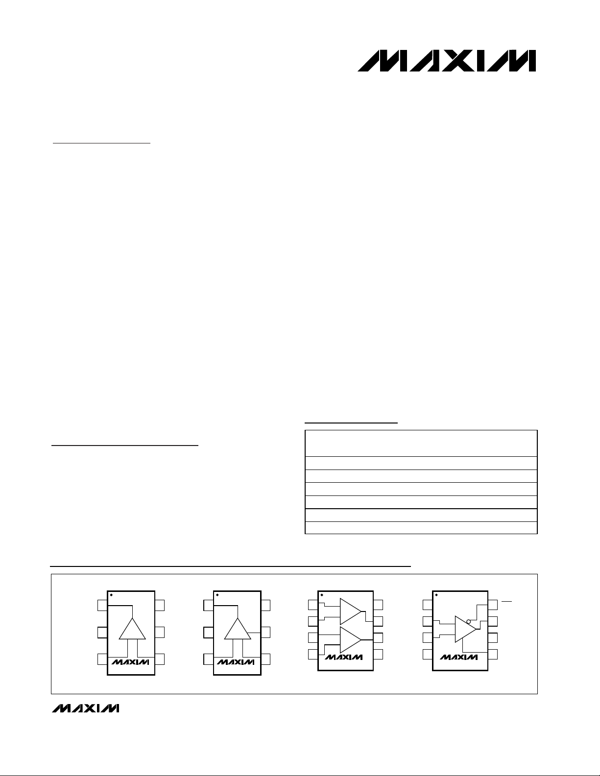
Pin Configurations
19-1932; Rev 1; 1/02
Ordering Information
Selector Guide appears at end of data sheet.
For pricing, delivery, and ordering information, please contact Maxim/Dallas Direct! at
1-888-629-4642, or visit Maxim’s website at www.maxim-ic.com.
PART TEMP RANGE
MAX9010EXT-T -40°C to +85°C 6 SC70-6 AAA
MAX9011EUT-T -40°C to +85°C 6 SOT23-6 AADD
MAX9012EUA -40°C to +85°C 8 µMAX —
MAX9012ESA -40°C to +85°C 8 SO —
MAX9013EUA -40°C to +85°C 8 µMAX —
MAX9013ESA -40°C to +85°C 8 SO —
PINPACKAGE
TOP
MARK
TOP VIEW
OUT
GND
1
16V
2
+ –
34
MAX9010
SC70
5V
OUT
CC
CC
IN-IN+
16V
GND
2
+ –
34
MAX9011
SOT23
5LE
INA+
CC
2
3
INB+
IN-IN+
4
+
_
+
_
MAX9012
SO/µMAX
87V
6
5
1
V
CC
CC
OUTAINA-
OUTB
GNDINB-
2
3
IN-
4
+
_
MAX9013
SO/µMAX
8
7 OUTIN+
6
5
OUT
GND
LEN.C.
Page 2
MAX9010–MAX9013
SC70, 5ns, Low-Power, Single-Supply,
Precision TTL Comparators
2 _______________________________________________________________________________________
ABSOLUTE MAXIMUM RATINGS
Stresses beyond those listed under “Absolute Maximum Ratings” may cause permanent damage to the device. These are stress ratings only, and functional
operation of the device at these or any other conditions beyond those indicated in the operational sections of the specifications is not implied. Exposure to
absolute maximum rating conditions for extended periods may affect device reliability.
Power Supply (VCCto GND) ...................................-0.3V to +6V
Analog Input (IN+ or IN-) to GND...............-0.3V to (V
CC
+ 0.3V)
Input Current (IN+ or IN-) .................................................±30mA
LE to GND ..................................................-0.3V to (V
CC
+ 0.3V)
Continuous Output Current...............................................±40mA
Continuous Power Dissipation (T
A
= +70°C)
6-Pin SC70 (derate 3.1mW/°C above +70°C).............245mW
6-Pin SOT23 (derate 8.7mW/°C above +70°C)...........696mW
8-Pin µMAX (derate 4.5mW/°C above +70°C) ............362mW
8-Pin SO (derate 5.9mW/°C above +70°C).................471mW
Operating Temperature Range ...........................-40°C to +85°C
Junction Temperature......................................................+150°C
Storage Temperature Range .............................-65°C to +150°C
Lead Temperature (soldering, 10s) .................................+300°C
ELECTRICAL CHARACTERISTICS (MAX9010/MAX9011)
(VCC= 5V, VLE= 0 (MAX9011 only), VCM= 0, TA= T
MIN
to T
MAX
, unless otherwise noted. Typical values are at TA= +25°C.) (Note 1)
)
Supply Voltage Range V
Power-Supply Current (Note 2)
Input Offset Voltage
(Note 3)
Input Offset-Voltage Drift
Input Bias Current I
Input Offset Current I
Differential Input Resistance
(Note 4)
Common-Mode Input
Resistance (Note 4)
Common-Mode Input Voltage
Range (Note 4)
Common-Mode Rejection
Ratio
PARAMETER SYMBOL CONDITIONS MIN TYP MAX UNITS
CC
I
CC
V
OS
∆V
∆T
OS/
B
OS
R
IN (D IFF) VIN(DIFF)
R
IN(CM
V
CM
CMRR -0.2V ≤ V
Power-Supply Rejection Ratio PSRR VCC = 4.5V to 5.5V 82 dB
Small-Signal Voltage Gain A
Output Low Voltage V
Output High Voltage V
Output Short-Circuit Current I
Latch Enable Pin High Input
Voltage
Latch Enable Pin Low Input
Voltage
Latch Enable Pin Bias Current IIH, I
OL
OH
OUT
V
IH
V
IL
V
IL
Inferred from VOS tests 4.5 5.5 V
TA = +25°C±1±5
T
T
A
to T
MIN
=
MAX
= ±10mV 250 kΩ
-0.2V ≤ VCM ≤ (VCC - 1.9V) 1 MΩ
Inferred from VOS tests -0.2 V
≤ (VCC - 1.9V) 95 dB
CM
1V ≤ V
≤ 2V 3000 V/V
OUT
VIN ≥ 100mV
VIN ≥ 100mV,
V
= 4.5V
CC
Sinking 20
Sourcing 30
MAX9011 only 2 V
MAX9011 only 0.8 V
MAX9011 only,
= 0 and VLE = 5V
V
LE
0.90 2.1 mA
±7
±2 µV /°C
±0.5 ±2 µA
±40 ±200 nA
- 1.9 V
CC
I
= 0 0.3 0.5
SINK
= 4mA 0.5 0.6
I
SINK
I
SOURCE
I
SOURCE
= 0 2.7 3.3
= 4mA 2.4 2.9
±25 µA
mV
V
V
mA
Page 3
MAX9010–MAX9013
SC70, 5ns, Low-Power, Single-Supply,
Precision TTL Comparators
_______________________________________________________________________________________ 3
ELECTRICAL CHARACTERISTICS (MAX9010/MAX9011) (continued)
(VCC= 5V, VLE= 0 (MAX9011 only), VCM= 0, TA= T
MIN
to T
MAX
, unless otherwise noted. Typical values are at TA= +25°C.) (Note 1)
ELECTRICAL CHARACTERISTICS (MAX9012/MAX9013)
(VCC= 5V, VLE= 0 (MAX9013 only), VCM= 0, TA= T
MIN
to T
MAX
, unless otherwise noted. Typical values are at TA= +25°C.) (Note 1)
)
Latch Setup Time (Note 8) t
Latch Hold Time (Note 8) t
Latch Propagation Delay
(Note 8)
Input Noise-Voltage Density e
Propagation Delay (Note 6) t
Output Rise Time t
Output Fall Time t
Input Capacitance C
Power-Up Time t
PARAMETER SYMBOL CONDITIONS MIN TYP MAX UNITS
SU
H
t
LPD
n
, t
PD+
PD-
R
F
IN
ON
MAX9011 only 2 0 ns
MAX9011 only 2 0.5 ns
MAX9011 only 5 ns
f = 100kHz 6 nV/√Hz
C
LOAD
T
+25°C
A
=
C
LOAD
T
T
MIN
A
=
0.5V ≤ V
2.5V ≥ V
V
= 5pF,
= 5pF,
to T
MAX V
≤ 2.5V 3 ns
OUT
≥ 0.5V 2 ns
OUT
OVERDRIVE
V
OVERDRIVE
V
OVERDRIVE
OVERDRIVE
= 100mV 5 8
= 5mV 5.5 9
= 100mV 9
= 5mV 10
MAX9010EXT 0.8
MAX9011EUT 1.2
ns
pF
1µs
Supply Voltage Range V
Power-Supply Current (Note 2) I
Input Offset Voltage
(Note 5)
Input Offset-Voltage Drift ∆V
Input Bias Current I
Input Offset Current I
Differential Input Resistance
(Note 4)
Common-Mode Input
Resistance (Note 4)
Common-Mode Input Voltage
Range (Note 4)
Common-Mode Rejection
Ratio
PARAMETER SYMBOL CONDITIONS MIN TYP MAX UNITS
CC
CC
V
OS
∆T±2µV /°C
OS/
B
OS
R
IN (D IFF)
R
IN(CM
V
CM
CMRR -0.2V ≤ V
Power-Supply Rejection Ratio PSRR VCC = 4.5V to 5.5V 63 82 dB
Inferred from PSRR test 4.5 5.5 V
MAX9012 2.4 4.2
MAX9013 1.3 2.3
TA = +25°C ±0.7 ±3
T
T
A
to T
MIN
=
MAX
±5.5
±0.5 ±2 µA
±40 ±200 nA
V
= ±10mV 250 kΩ
IN(DIFF)
-0.2V ≤ VCM ≤ (VCC - 1.9V) 1 MΩ
Inferred from CMRR test -0.2 V
≤ (VCC - 1.9V) 75 95 dB
CM
- 1.9 V
CC
mA
mV
Page 4
MAX9010–MAX9013
SC70, 5ns, Low-Power, Single-Supply,
Precision TTL Comparators
4 _______________________________________________________________________________________
ELECTRICAL CHARACTERISTICS (MAX9012/MAX9013) (continued)
(VCC= 5V, VLE= 0 (MAX9013 only), VCM= 0, TA= T
MIN
to T
MAX
, unless otherwise noted. Typical values are at TA= +25°C.) (Note 1)
)
Note 1: All specifications are 100% tested at TA= +25°C; temperature limits are guaranteed by design.
Note 2: Quiescent Power-Supply Current is slightly higher with the comparator output at V
OL
. This parameter is specified with the worst-
case condition of V
OUT
= VOLfor the MAX9010/MAX9011 and both outputs at VOLfor the MAX9012. For the MAX9013, which
has complementary outputs, the power-supply current is specified with either OUT = V
OL
, OUT = VOHor OUT = VOH, OUT =
V
OL
(power-supply current is equal in either case).
Note 3: Input Offset Voltage is tested and specified with the Input Common-Mode Voltage set to either extreme of the Input Common-
Mode Voltage Range (-0.2V to (V
CC
- 1.9V)) and with the Power-Supply Voltage set to either extreme of the Power-Supply
Voltage Range (4.5V to 5.5V).
Small-Signal Voltage Gain A
Output Low Voltage V
Output High Voltage V
Output Short-Circuit Current I
Latch Enable Pin High Input
Voltage
Latch Enable Pin Low Input
Voltage
Latch Enable Pin Bias Current IIH, I
Input Noise-Voltage Density e
Propagation Delay (Note 6) t
Differential Propagation Delay
(Notes 6, 7)
Channel-to-Channel
Propagation Delay (Note 6)
Output Rise Time t
Output Fall Time t
Latch Setup Time (Note 8) t
Latch Hold Time (Note 8) t
Latch Propagation Delay
(Note 8)
Input Capacitance C
Power-Up Time t
PARAMETER SYMBOL CONDITIONS MIN TYP MAX UNITS
V
OL
OH
OUT
V
IH
V
IL
IL
n
, t
PD+
PD-
∆t
PD±
∆t
PD(ch-ch
R
F
SU
H
t
LPD
IN
ON
1V ≤ V
OUT
VIN ≥ 100mV
VIN ≥ 100mV,
= 4.5V
V
CC
≤ 2V 1000 3000 V/V
I
= 0 0.3 0.5
SINK
I
= 4mA 0.5 0.6
SINK
I
SOURCE
I
SOURCE
= 0 2.7 3.3
= 4mA 2.4 2.9
Sinking 20
Sourcing 30
MAX9013 only 2 V
MAX9013 only 0.8 V
MAX9013 only
0 and VLE = 5V
V
LE
=
f = 100kHz 6 nV/√Hz
C
= 5pF,
LOAD
+25°C
T
A
=
C
= 5pF,
LOAD
to T
T
T
A
=
MIN
MAX V
VIN = 100mV step, C
= 5mV
V
OD
V
OVERDRIVE
V
OVERDRIVE
V
OVERDRIVE
OVERDRIVE
LOAD
= 100mV 5 8
= 5mV 5.5 9
= 100mV 9
= 5mV 10
= 5pF,
MAX9012 only, VIN = 100mV step,
= 5pF, VOD = 5mV
C
LOAD
0.5V ≤ V
2.5V ≥ V
≤ 2.5V 3 ns
OUT
≥ 0.5V 2 ns
OUT
MAX9013 only 2 0 ns
MAX9013 only 2 0.5 ns
MAX9013 only 5 ns
MAX9012EUA/MAX9013EUA 1.5
MAX9012ESA/MAX9013ESA 2
V
V
mA
±25 µA
ns
23ns
500 ps
pF
1µs
Page 5

MAX9010–MAX9013
SC70, 5ns, Low-Power, Single-Supply,
Precision TTL Comparators
_______________________________________________________________________________________ 5
Note 4: Although Common-Mode Input Voltage Range is restricted to -0.2V ≤ VCM≤ (VCC- 1.9V), either or both inputs can go to either
absolute maximum voltage limit, i.e., from -0.3V to (V
CC
+ 0.3V), without damage. The comparator will make a correct (and fast)
logic decision provided that at least one of the two inputs is within the specified common-mode range. If both inputs are outside
the common-mode range, the comparator output state is indeterminate.
Note 5: For the MAX9012, Input Offset Voltage is defined as the input voltage(s) required to make the OUT output voltage(s) remain
stable at 1.4V. For the MAX9013, it is defined as the average of two input offset voltages, measured by forcing first the OUT
output, then the OUT output to 1.4V.
Note 6: Propagation delay for these high-speed comparators is guaranteed by design because it cannot be accurately measured
with low levels of input overdrive voltage using automatic test equipment in production. Note that for low overdrive
conditions, V
OS
is added to the overdrive.
Note 7: Differential Propagation Delay, measured either on a single output of the MAX9012/MAX9013 (or between OUT and OUT
outputs on the MAX9013) is defined as: ∆t
PD(±)
= |(t
PD+
) - (t
PD-
)|.
Note 8: Latch times are guaranteed by design. Latch setup time (t
SU
) is the interval in which the input signal must be stable prior to
asserting the latch signal. The hold time (t
H
) is the interval after the latch is asserted in which the input signal must remain
stable. Latch propagation delay (t
LPD
) is the delay time for the output to respond when the latch enable pin is deasserted
(see Figure 1).
t = 5ns/div
RESPONSE TO -5mV OVERDRIVE
IN: 50mV/div
OUT: 1V/div
0
IN
3V
+100mV
MAX9010–13 toc02
OUT
0
6.0
3.5
1 10 100
4.0
MAX9010–13 toc03
OVERDRIVE (mV)
PROPAGATION DELAY (ns)
4.5
5.0
5.5
PROPAGATION DELAY
vs. INPUT OVERDRIVE
3.0
t
PD(+)
t
PD(-)
t = 5ns/div
RESPONSE TO +5mV OVERDRIVE
IN: 50mV/div
OUT: 1V/div
0
IN
3V
-100mV
MAX9010–13 toc01
OUT
0
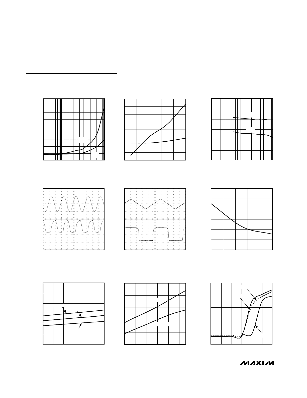
Typical Operating Characteristics
(VCC= 5V, CL= 15pF, TA = +25°C, unless otherwise noted.)
Page 6
MAX9010–MAX9013
SC70, 5ns, Low-Power, Single-Supply,
Precision TTL Comparators
6 _______________________________________________________________________________________
Typical Operating Characteristics (continued)
(VCC= 5V, CL= 15pF, TA = +25°C, unless otherwise noted.)
0
10 10k1k100
PROPAGATION DELAY
vs. SOURCE RESISTANCE
15
5
35
25
45
20
10
40
30
MAX9010–13 toc04
SOURCE RESISTANCE (Ω)
PROPAGATION DELAY (ns)
t
PD(+)
t
PD(-)
4.0
4.5
5.0
5.5
6.0
6.5
7.0
7.5
8.0
10 20 30 40 50 60
PROPAGATION DELAY
vs. LOAD CAPACITANCE
MAX9010–13 toc05
LOAD CAPACITANCE (pF)
PROPAGATION DELAY (ns)
t
PD(+)
t
PD(-)
6.0
3.5
1 10 100
4.0
MAX9010–13 toc03
OVERDRIVE (mV)
PROPAGATION DELAY (ns)
4.5
5.0
5.5
PROPAGATION DELAY
vs. INPUT OVERDRIVE
3.0
t
PD(+)
t
PD(-)
RESPONSE TO 50MHz ±10mV
SINE WAVE
MAX9010–13 toc07
10ns/div
A
0
B
0
A: Input, 10mV/div
B: Output, 2V/div
RESPONSE TO 10kHz TRIANGLE WAVE
MAX9010–13 toc08
20µs/div
A
0
B
0
A: Input, 20mV/div
B: Output, 2V/div
-0.9
-0.7
-0.8
-0.5
-0.6
-0.4
-0.3
-40 10-15 35 60 85
OFFSET VOLTAGE
vs. TEMPERATURE
MAX9010–13 toc09
TEMPERATURE (°C)
OFFSET VOLTAGE (mV)
0
0.5
1.5
1.0
2.0
2.5
-3 -1 0-2 1 2 3
OUTPUT VOLTAGE vs.
DIFFERENTIAL INPUT VOLTAGE
DIFFERENTIAL INPUT VOLTAGE (mV)
OUTPUT VOLTAGE (V)
MAX9010–13 toc12
TA = +25°C
TA = +85°C
TA = -40°C
0.2
0.3
0.5
0.4
0.6
0.7
-40 10 35-15 60 85
INPUT BIAS CURRENT vs. TEMPERATURE
MAX9010–13 toc11
TEMPERATURE (°C )
INPUT BIAS CURRENT (µA)
VCM = -0.2V
VCM = 3.1V
SUPPLY CURRENT vs. SUPPLY VOLTAGE
(PER COMPARATOR)
MAX9010–13 toc10
VCC (V)
I
CC
(mA)
5.755.505.255.004.75
0.5
1.0
1.5
2.0
2.5
3.0
0
4.50 6.00
TA = +85°C
TA = +25°C
TA = -40°C
Page 7

MAX9010–MAX9013
SC70, 5ns, Low-Power, Single-Supply,
Precision TTL Comparators
_______________________________________________________________________________________ 7
Detailed Description
These high-speed comparators have a unique design
that prevents oscillation when the comparator is in its
linear region, so no minimum input slew rate is required.
Many high-speed comparators oscillate in their linear
region. One common way to overcome this oscillation is
to add hysteresis, but it results in a loss of resolution
and bandwidth.
Latch Function
The MAX9011/MAX9013 provide a TTL-compatible latch
function that holds the comparator output state (Figure 1).
With LE driven to a TTL low or grounded, the latch is
transparent and the output state is determined by the
input differential voltage. When LE is driven to a TTL high,
the existing output state is latched, and the input differential voltage has no further effect on the output state.
Input Amplifier
A comparator can be thought of as having two sections: an input amplifier and a logic interface. The input
amplifiers of these devices are fully differential, with
input offset voltages typically 0.7mV at +25°C. Input
common-mode range extends from 200mV below
ground to 1.9V below the positive power-supply rail. The
total common-mode range is 3.3V when operating from a
5V supply. The amplifiers have no built-in hysteresis. For
highest accuracy, do not add hysteresis. Figure 2 shows
how hysteresis degrades resolution.
Input Voltage Range
Although the common-mode input voltage range is
restricted to -0.2V to (V
CC
- 1.9V), either or both inputs
can go to either absolute maximum voltage limit, i.e.,
from -0.3V to (V
CC
+ 0.3V), without damage. The comparator will make a correct (and fast) logic decision
provided that at least one of the two inputs is within the
specified common-mode range. If both inputs are outside the common-mode range, the comparator output
state is indeterminate.
Resolution
A comparator’s ability to resolve a small-signal difference, its resolution, is affected by various factors. As
with most amplifiers and comparators, the most significant factors are the input offset voltage (VOS) and the
common-mode and power-supply rejection ratios
(CMRR, PSRR). If source impedance is high, input offset current can be significant. If source impedance is
unbalanced, the input bias current can introduce
another error. For high-speed comparators, an addi-
Pin Description
PIN
MAX9010 MAX9011 MAX9012 MAX9013
11— 7 OUT
2 2 5 6 GND Ground
33— 2 IN+ Noninverting Input
44— 3 IN- Inverting Input
5, 6 6 8 1 V
— 5 — 5 LE Latch Enable Input
—— 1 — INA+ Noninverting Input, Channel A
—— 2 — INA- Inverting Input, Channel A
—— 3 — INB+ Noninverting Input, Channel B
—— 4 — INB- Inverting Input, Channel B
—— 6 — OUTB Comparator Output, Channel B
—— 7 — OUTA Comparator Output, Channel A
——— 4 N.C.
——— 8 OUT Comparator Complementary Output
NAME FUNCTION
Comparator Output. OUT is high when IN+ is more
positive than IN-.
Positive Power-Supply Voltage. Pins 5 and 6 of the
CC
MAX9010 must BOTH be connected to the powersupply rail. Bypass with a 0.1µF capacitor.
No Connection. Not internally connected. Connect to
GND for best results.
Page 8

MAX9010–MAX9013
SC70, 5ns, Low-Power, Single-Supply,
Precision TTL Comparators
8 _______________________________________________________________________________________
tional factor in resolution is the comparator’s stability in
its linear region. Many high-speed comparators are
useless in their linear region because they oscillate.
This makes the differential input voltage region around
zero unusable. Hysteresis helps to cure the problem
but reduces resolution (Figure 2). The devices do not
oscillate in the linear region and require no hysteresis,
which greatly enhances their resolution.
Applications Information
Power Supplies, Bypassing, and
Board Layout
These products operate over a supply voltage range of
4.5V to 5.5V. Bypass VCCto GND with a 0.1µF surfacemount ceramic capacitor. Mount the ceramic capacitor
as close as possible to the supply pin to minimize lead
inductance.
As with all high-speed components, careful attention to
board layout is essential for best performance. Use a
PC board with an unbroken ground plane. Pay close
attention to the bandwidth of bypass components and
place them as close as possible to the device.
Minimize the trace length and area at the comparator
inputs. If the source impedance is high, take the utmost
care in minimizing its susceptibility to pickup of unwanted signals.
Input Slew Rate
Most high-speed comparators have a minimum input
slew-rate requirement. If the input signal does not
transverse the region of instability within a propagation
delay of the comparator, the output can oscillate. This
makes many high-speed comparators unsuitable for
processing either slow-moving signals or fast-moving
signals with low overdrive. The design of these devices
eliminates the minimum input slew-rate requirement.
They are excellent for circuits from DC up to 200MHz,
even with very low overdrive, where small signals need
to be resolved.
Figure 1. Timing Diagram
Figure 2. Effect of Hysteresis on Input Resolution
t
SU
V
LATCH
ENABLE (LE)
IN+
IN
OUT
t
H
t
PD+
(DIFFERENTIAL)
IN-
OUT
WITH HYSTERESIS
IDEAL (WITHOUT HYSTERESIS)
* WHEN HYSTERESIS IS ADDED, A COMPARATOR CANNOT RESOLVE ANY INPUT SIGNAL WITHIN THE HYSTERESIS BAND.
HYSTERESIS
BAND*
Page 9

Chip Information
MAX9010 TRANSISTOR COUNT: 106
MAX9011 TRANSISTOR COUNT: 137
MAX9012 TRANSISTOR COUNT: 212
MAX9013 TRANSISTOR COUNT: 145
PROCESS: Bipolar
MAX9010–MAX9013
SC70, 5ns, Low-Power, Single-Supply,
Precision TTL Comparators
_______________________________________________________________________________________ 9
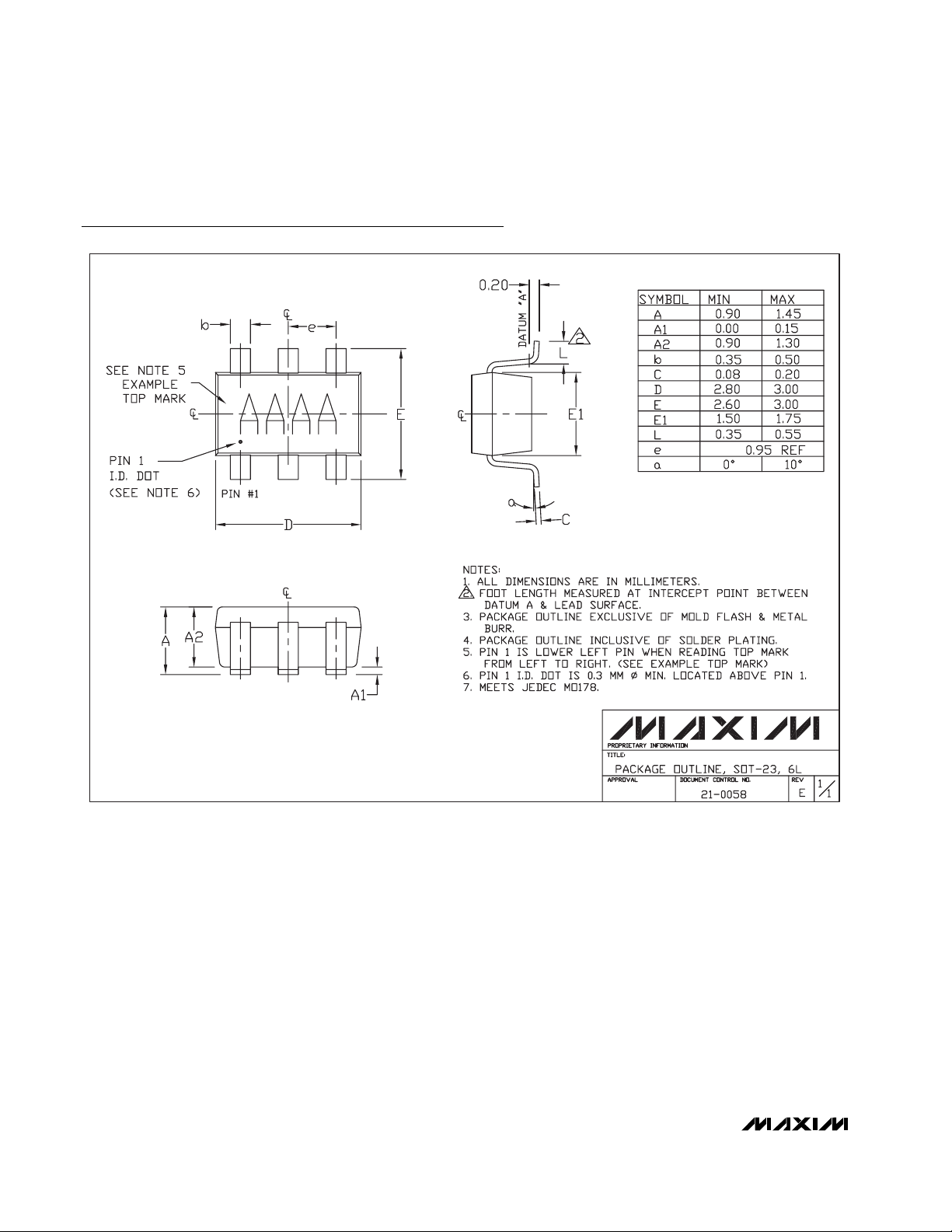
Package Information
Selector Guide
PART COMPARATORS LATCH
MAX9010 1 No No
MAX9011 1 Yes No
MAX9012 2 No No
MAX9013 1 Yes Yes
COMPLEMENTARY
OUTPUTS
SC70, 6L.EPS
Page 10
MAX9010–MAX9013
SC70, 5ns, Low-Power, Single-Supply,
Precision TTL Comparators
10 ______________________________________________________________________________________
Package Information (continued)
6LSOT.EPS
Page 11

MAX9010–MAX9013
SC70, 5ns, Low-Power, Single-Supply,
Precision TTL Comparators
______________________________________________________________________________________ 11
Package Information (continued)
8LUMAXD.EPS
Page 12

MAX9010–MAX9013
SC70, 5ns, Low-Power, Single-Supply,
Precision TTL Comparators
Maxim cannot assume responsibility for use of any circuitry other than circuitry entirely embodied in a Maxim product. No circuit patent licenses are
implied. Maxim reserves the right to change the circuitry and specifications without notice at any time.
12 ____________________Maxim Integrated Products, 120 San Gabriel Drive, Sunnyvale, CA 94086 408-737-7600
© 2002 Maxim Integrated Products Printed USA is a registered trademark of Maxim Integrated Products.
Package Information (continued)
SOICN.EPS
 Loading...