

Page 1

19-5472; Rev 1; 1/11
EVALUATION KIT
AVAILABLE
Power-Management ICs for
ICERA E400/E450 Platform
General Description
The MAX8982A/MAX8982X are complete power-management ICs for the latest LTE/WCDMA/GSM/GPRS/
EDGE data card based on the new ICERA platform (E400/
E450). The MAX8982A operates from a 4.1V to 5.5V
supply and contains four efficient step-down converters,
nine low dropout linear regulators (LDOs) to power all
RF and baseband circuitry, three current regulators with
programmable current up to 24mA and embedded flash
timers, and an I
regulator output voltages as well as on/off control for flexibility. The linear regulators provide greater than 60dB
PSRR, less than 45FV of output noise, and minimal cross
coupling noise between LDOs.
The MAX8982X operates from a 2.9V to 5.5V supply. The
MAX8982X has the same features as the MAX8982A,
except it does not have BUCK3, BUCK4, and LDO8.
All buck converters and LDOs are enabled/disabled by
either I
This feature provides more flexibility in system design.
2
C or PWR_REQ control signal after power-up.
Applications
GSM, GPRS, EDGE, WCDMA, and LTE
Data Card with New ICERA Platform (E400/E450)
Ordering Information
PART TEMP RANGE PIN-PACKAGE
MAX8982AEWO+T -40°C to +85°C 42 WLP
MAX8982XEWO+T -40°C to +85°C 42 WLP
+Denotes a lead(Pb)-free/RoHS-compliant package.
T = Tape and reel. These devices have a minimum order inc-
rement of 1k pieces.
2
C serial interface to program individual
Features
S 4 High-Efficiency Buck Converters
0.9V at 1.2A for CORE with DVS Function (0.6V
to 1.2V in 25mV Steps) and Slew Rate Control
1.8V at 600mA for System IO
3.2V at 600mA for All LDO Inputs (2.9V to 3.65V
in 50mV Steps) (MAX8982A Only)
3.4V at 1.8A for GSM/WCDMA PA (3.0V to 3.75V
in 50mV Steps) (MAX8982A Only)
9 LDO Linear Regulators
S
2.7V at 300mA on LDO1 for RF Transceiver
1.8V at 150mA on LDO2 for RF Transceiver
2.8V at 150mA on LDO3 for Analogue BB
0.9V at 50mA on LDO4 for BB PLL with the
Separate Input for a Higher Efficiency
3.0V at 150mA on LDO5 for SD Card
2.7V at 150mA on LDO6 for TCXO
1.8V or 3.0V at 150mA on LDO7 for SIM
3.0V at 150mA on LDO8 for USB with the
Separate Input (MAX8982A Only)
0.9V at 50mA on LDO9 for BB with the Separate
Input for a Higher Efficiency
32 Programmable Voltage Options and External
S
Input on BUCK1 (0.9V Default) for DVS
S 16 Programmable Voltage Options for BUCK3
(MAX8982A Only)
S 16 Programmable Voltage Options on BUCK4
(MAX8982A Only)
S Programmable Voltage Options for All LDOs
(LDO8 for MAX8982A Only)
S BUCK2, BUCK3 (MAX8982A Only), LDO3, and
Internal 32kHz Clock Default On at Initial Startup
S Some Buck Converters and LDOs are Enabled by
Either I
After Power-Up
S 3 Current Regulators with 8 Dimming Current
Options Up to 24mA with Embedded Flash Timer
2
C or Power Request Control (PWR_REQ)
MAX8982A/MAX8982X
_______________________________________________________________ Maxim Integrated Products 1
For pricing, delivery, and ordering information, please contact Maxim Direct at 1-888-629-4642,
or visit Maxim’s website at www.maxim-ic.com.
Page 2

Power-Management ICs for
ICERA E400/E450 Platform
Table of ConTenTs
General Description . . . . . . . . . . . . . . . . . . . . . . . . . . . . . . . . . . . . . . . . . . . . . . . . . . . . . . . . . . . . . . . . . . . . . . . . . . . . 1
Applications . . . . . . . . . . . . . . . . . . . . . . . . . . . . . . . . . . . . . . . . . . . . . . . . . . . . . . . . . . . . . . . . . . . . . . . . . . . . . . . . . . 1
Features . . . . . . . . . . . . . . . . . . . . . . . . . . . . . . . . . . . . . . . . . . . . . . . . . . . . . . . . . . . . . . . . . . . . . . . . . . . . . . . . . . . . . 1
Ordering Information . . . . . . . . . . . . . . . . . . . . . . . . . . . . . . . . . . . . . . . . . . . . . . . . . . . . . . . . . . . . . . . . . . . . . . . . . . . 1
Absolute Maximum Ratings . . . . . . . . . . . . . . . . . . . . . . . . . . . . . . . . . . . . . . . . . . . . . . . . . . . . . . . . . . . . . . . . . . . . . . 7
General Electrical Characteristics . . . . . . . . . . . . . . . . . . . . . . . . . . . . . . . . . . . . . . . . . . . . . . . . . . . . . . . . . . . . . . . . . 7
Buck1 Electrical Characteristics. . . . . . . . . . . . . . . . . . . . . . . . . . . . . . . . . . . . . . . . . . . . . . . . . . . . . . . . . . . . . . . . . . . 9
Buck2 Electrical Characteristics. . . . . . . . . . . . . . . . . . . . . . . . . . . . . . . . . . . . . . . . . . . . . . . . . . . . . . . . . . . . . . . . . . 10
Buck3 Electrical Characteristics. . . . . . . . . . . . . . . . . . . . . . . . . . . . . . . . . . . . . . . . . . . . . . . . . . . . . . . . . . . . . . . . . . 10
Buck4 Electrical Characteristics. . . . . . . . . . . . . . . . . . . . . . . . . . . . . . . . . . . . . . . . . . . . . . . . . . . . . . . . . . . . . . . . . . 11
OUT1 (LDO1) Electrical Characteristics . . . . . . . . . . . . . . . . . . . . . . . . . . . . . . . . . . . . . . . . . . . . . . . . . . . . . . . . . . . . 12
OUT2 (LDO2) Electrical Characteristics. . . . . . . . . . . . . . . . . . . . . . . . . . . . . . . . . . . . . . . . . . . . . . . . . . . . . . . . . . . . 12
OUT3 (LDO3) Electrical Characteristics. . . . . . . . . . . . . . . . . . . . . . . . . . . . . . . . . . . . . . . . . . . . . . . . . . . . . . . . . . . . 13
OUT4 (LDO4) Electrical Characteristics . . . . . . . . . . . . . . . . . . . . . . . . . . . . . . . . . . . . . . . . . . . . . . . . . . . . . . . . . . . . 14
MAX8982A/MAX8982X
OUT5 (LDO5) Electrical Characteristics. . . . . . . . . . . . . . . . . . . . . . . . . . . . . . . . . . . . . . . . . . . . . . . . . . . . . . . . . . . . 14
OUT6 (LDO6) Electrical Characteristics. . . . . . . . . . . . . . . . . . . . . . . . . . . . . . . . . . . . . . . . . . . . . . . . . . . . . . . . . . . . 15
VSIM (LDO7) Electrical Characteristics . . . . . . . . . . . . . . . . . . . . . . . . . . . . . . . . . . . . . . . . . . . . . . . . . . . . . . . . . . . . 15
OUT8 (LDO8) Electrical Characteristics. . . . . . . . . . . . . . . . . . . . . . . . . . . . . . . . . . . . . . . . . . . . . . . . . . . . . . . . . . . . 16
OUT9 (LDO9) Electrical Characteristics. . . . . . . . . . . . . . . . . . . . . . . . . . . . . . . . . . . . . . . . . . . . . . . . . . . . . . . . . . . . 16
RESET Electrical Characteristics . . . . . . . . . . . . . . . . . . . . . . . . . . . . . . . . . . . . . . . . . . . . . . . . . . . . . . . . . . . . . . . . . 17
IRQ Electrical Characteristics. . . . . . . . . . . . . . . . . . . . . . . . . . . . . . . . . . . . . . . . . . . . . . . . . . . . . . . . . . . . . . . . . . . . 17
Current Regulator Electrical Characteristics. . . . . . . . . . . . . . . . . . . . . . . . . . . . . . . . . . . . . . . . . . . . . . . . . . . . . . . . . 17
Flash Timer Electrical Characteristics . . . . . . . . . . . . . . . . . . . . . . . . . . . . . . . . . . . . . . . . . . . . . . . . . . . . . . . . . . . . . 18
N32kHz Electrical Characteristics . . . . . . . . . . . . . . . . . . . . . . . . . . . . . . . . . . . . . . . . . . . . . . . . . . . . . . . . . . . . . . . . 19
Typical Operating Characteristics . . . . . . . . . . . . . . . . . . . . . . . . . . . . . . . . . . . . . . . . . . . . . . . . . . . . . . . . . . . . . . . . 19
Pin Configurations . . . . . . . . . . . . . . . . . . . . . . . . . . . . . . . . . . . . . . . . . . . . . . . . . . . . . . . . . . . . . . . . . . . . . . . . . . . . 25
Pin Description . . . . . . . . . . . . . . . . . . . . . . . . . . . . . . . . . . . . . . . . . . . . . . . . . . . . . . . . . . . . . . . . . . . . . . . . . . . . . . . 27
Detailed Description . . . . . . . . . . . . . . . . . . . . . . . . . . . . . . . . . . . . . . . . . . . . . . . . . . . . . . . . . . . . . . . . . . . . . . . . . . . 34
Power-On/Off Control . . . . . . . . . . . . . . . . . . . . . . . . . . . . . . . . . . . . . . . . . . . . . . . . . . . . . . . . . . . . . . . . . . . . . . . . 34
PWR_REQ . . . . . . . . . . . . . . . . . . . . . . . . . . . . . . . . . . . . . . . . . . . . . . . . . . . . . . . . . . . . . . . . . . . . . . . . . . . . . . 34
Active Discharge . . . . . . . . . . . . . . . . . . . . . . . . . . . . . . . . . . . . . . . . . . . . . . . . . . . . . . . . . . . . . . . . . . . . . . . . . . . . 35
BUCK1, BUCK2, and BUCK3
Step-Down Converters . . . . . . . . . . . . . . . . . . . . . . . . . . . . . . . . . . . . . . . . . . . . . . . . . . . . . . . . . . . . . . . . . . . . . . . 37
Setting the Output Voltage on BUCK1 . . . . . . . . . . . . . . . . . . . . . . . . . . . . . . . . . . . . . . . . . . . . . . . . . . . . . . . . . . . 37
Dynamic Voltage Scaling (DVS) Function on Buck 1 . . . . . . . . . . . . . . . . . . . . . . . . . . . . . . . . . . . . . . . . . . . . . . . . 37
2
Page 3

Power-Management ICs for
ICERA E400/E450 Platform
Table of ConTenTs (ConTinued)
Ramp-Up/Down Slope Control on BUCK1 . . . . . . . . . . . . . . . . . . . . . . . . . . . . . . . . . . . . . . . . . . . . . . . . . . . . . . . . 38
Setting the Output Voltage on BUCK2 . . . . . . . . . . . . . . . . . . . . . . . . . . . . . . . . . . . . . . . . . . . . . . . . . . . . . . . . . . . 38
Setting the Output Voltage on BUCK3 . . . . . . . . . . . . . . . . . . . . . . . . . . . . . . . . . . . . . . . . . . . . . . . . . . . . . . . . . . . 38
BUCK4 Step-Down Converter for PA (Power Amplifier) . . . . . . . . . . . . . . . . . . . . . . . . . . . . . . . . . . . . . . . . . . . . . .38
Setting the Output Voltage on BUCK4 . . . . . . . . . . . . . . . . . . . . . . . . . . . . . . . . . . . . . . . . . . . . . . . . . . . . . . . . . . . 38
Linear Regulators . . . . . . . . . . . . . . . . . . . . . . . . . . . . . . . . . . . . . . . . . . . . . . . . . . . . . . . . . . . . . . . . . . . . . . . . . . . 38
Reference Bypass (REFBP) . . . . . . . . . . . . . . . . . . . . . . . . . . . . . . . . . . . . . . . . . . . . . . . . . . . . . . . . . . . . . . . . . . . 38
Thermal Overload Protection. . . . . . . . . . . . . . . . . . . . . . . . . . . . . . . . . . . . . . . . . . . . . . . . . . . . . . . . . . . . . . . . . . . 38
Undervoltage Lockout (UVLO) . . . . . . . . . . . . . . . . . . . . . . . . . . . . . . . . . . . . . . . . . . . . . . . . . . . . . . . . . . . . . . . . . 38
Overvoltage Protection (OVP) . . . . . . . . . . . . . . . . . . . . . . . . . . . . . . . . . . . . . . . . . . . . . . . . . . . . . . . . . . . . . . . . . . 38
Power-On Reset (POR) . . . . . . . . . . . . . . . . . . . . . . . . . . . . . . . . . . . . . . . . . . . . . . . . . . . . . . . . . . . . . . . . . . . . . . . 38
Current Regulators (DR1, DR2, DR3) . . . . . . . . . . . . . . . . . . . . . . . . . . . . . . . . . . . . . . . . . . . . . . . . . . . . . . . . . . . .39
Embedded Flash Timer. . . . . . . . . . . . . . . . . . . . . . . . . . . . . . . . . . . . . . . . . . . . . . . . . . . . . . . . . . . . . . . . . . . . . . . 39
IRQ Description. . . . . . . . . . . . . . . . . . . . . . . . . . . . . . . . . . . . . . . . . . . . . . . . . . . . . . . . . . . . . . . . . . . . . . . . . . . . .39
RESET SIGNAL to B/B Chipset. . . . . . . . . . . . . . . . . . . . . . . . . . . . . . . . . . . . . . . . . . . . . . . . . . . . . . . . . . . . . . . . . 40
2
C Serial Interface . . . . . . . . . . . . . . . . . . . . . . . . . . . . . . . . . . . . . . . . . . . . . . . . . . . . . . . . . . . . . . . . . . . . . . . . . .40
I
Bit Transfer . . . . . . . . . . . . . . . . . . . . . . . . . . . . . . . . . . . . . . . . . . . . . . . . . . . . . . . . . . . . . . . . . . . . . . . . . . . . . . 40
START and STOP Conditions. . . . . . . . . . . . . . . . . . . . . . . . . . . . . . . . . . . . . . . . . . . . . . . . . . . . . . . . . . . . . . . . 40
System Configuration . . . . . . . . . . . . . . . . . . . . . . . . . . . . . . . . . . . . . . . . . . . . . . . . . . . . . . . . . . . . . . . . . . . . . . 41
Acknowledge . . . . . . . . . . . . . . . . . . . . . . . . . . . . . . . . . . . . . . . . . . . . . . . . . . . . . . . . . . . . . . . . . . . . . . . . . . . . 41
Slave Address . . . . . . . . . . . . . . . . . . . . . . . . . . . . . . . . . . . . . . . . . . . . . . . . . . . . . . . . . . . . . . . . . . . . . . . . . . .42
Write Operations. . . . . . . . . . . . . . . . . . . . . . . . . . . . . . . . . . . . . . . . . . . . . . . . . . . . . . . . . . . . . . . . . . . . . . . . . . 42
Read Operations . . . . . . . . . . . . . . . . . . . . . . . . . . . . . . . . . . . . . . . . . . . . . . . . . . . . . . . . . . . . . . . . . . . . . . . . .43
Applications Information. . . . . . . . . . . . . . . . . . . . . . . . . . . . . . . . . . . . . . . . . . . . . . . . . . . . . . . . . . . . . . . . . . . . . . . . 69
Inductor Selection . . . . . . . . . . . . . . . . . . . . . . . . . . . . . . . . . . . . . . . . . . . . . . . . . . . . . . . . . . . . . . . . . . . . . . . . . . . 69
Output Capacitor Selection . . . . . . . . . . . . . . . . . . . . . . . . . . . . . . . . . . . . . . . . . . . . . . . . . . . . . . . . . . . . . . . . . . . . 71
Input Capacitor Selection . . . . . . . . . . . . . . . . . . . . . . . . . . . . . . . . . . . . . . . . . . . . . . . . . . . . . . . . . . . . . . . . . . . . . 71
PCB Layout Guidelines . . . . . . . . . . . . . . . . . . . . . . . . . . . . . . . . . . . . . . . . . . . . . . . . . . . . . . . . . . . . . . . . . . . . . . . 71
Chip Information . . . . . . . . . . . . . . . . . . . . . . . . . . . . . . . . . . . . . . . . . . . . . . . . . . . . . . . . . . . . . . . . . . . . . . . . . . . . . . 71
Package Information. . . . . . . . . . . . . . . . . . . . . . . . . . . . . . . . . . . . . . . . . . . . . . . . . . . . . . . . . . . . . . . . . . . . . . . . . . . 72
Revision History . . . . . . . . . . . . . . . . . . . . . . . . . . . . . . . . . . . . . . . . . . . . . . . . . . . . . . . . . . . . . . . . . . . . . . . . . . . . . . 73
MAX8982A/MAX8982X
3
Page 4

Power-Management ICs for
ICERA E400/E450 Platform
Table of ConTenTs (ConTinued)
List of Figures
Figure 1. MAX8982A Typical Application Circuit and Functional Block Diagram . . . . . . . . . . . . . . . . . . . . . . . . . . . . 31
Figure 2. MAX8982X Typical Application Circuit and Functional Block Diagram . . . . . . . . . . . . . . . . . . . . . . . . . . . . 33
Figure 3. Power-On/Off State Diagram with IN3 Connected to BUCK2 Output and IN4 Connected to IN1_.
Default PWR_REQ Regulators Are Shown.. . . . . . . . . . . . . . . . . . . . . . . . . . . . . . . . . . . . . . . . . . . . . . . . . . 35
Figure 4. MAX8982A/MAX8982X Power-On Timing Diagram at Initial Startup with EN Connected to IN1_.
BUCK3 and OUT8 Are for the MAX8982A Only. . . . . . . . . . . . . . . . . . . . . . . . . . . . . . . . . . . . . . . . . . . . . . 36
Figure 5. MAX8982A/MAX8982X Power-On Timing Diagram in PWR_REQ ON Mode After Power-Up . . . . . . . . . . 37
Figure 6. Frequency Variation vs. Load Current with a 5V Input Supply . . . . . . . . . . . . . . . . . . . . . . . . . . . . . . . . . . . 37
Figure 7. DVS1 Logic Diagram . . . . . . . . . . . . . . . . . . . . . . . . . . . . . . . . . . . . . . . . . . . . . . . . . . . . . . . . . . . . . . . . . . . 37
Figure 8. BUCK1 Ramp-Up/Down Slope Control. . . . . . . . . . . . . . . . . . . . . . . . . . . . . . . . . . . . . . . . . . . . . . . . . . . . . 38
Figure 9. POR State Diagram. . . . . . . . . . . . . . . . . . . . . . . . . . . . . . . . . . . . . . . . . . . . . . . . . . . . . . . . . . . . . . . . . . . . 39
Figure 10. Adding Series Resistors to Adjust LED Current . . . . . . . . . . . . . . . . . . . . . . . . . . . . . . . . . . . . . . . . . . . . . 39
Figure 11. Flash Timing Diagram . . . . . . . . . . . . . . . . . . . . . . . . . . . . . . . . . . . . . . . . . . . . . . . . . . . . . . . . . . . . . . . . . 39
MAX8982A/MAX8982X
Figure 12. I
Figure 13. START and STOP Conditions . . . . . . . . . . . . . . . . . . . . . . . . . . . . . . . . . . . . . . . . . . . . . . . . . . . . . . . . . . . 40
Figure 14. Master/Slave Configuration . . . . . . . . . . . . . . . . . . . . . . . . . . . . . . . . . . . . . . . . . . . . . . . . . . . . . . . . . . . . . 41
Figure 15. I
Figure 16. I
Figure 17. Writing to the ICs . . . . . . . . . . . . . . . . . . . . . . . . . . . . . . . . . . . . . . . . . . . . . . . . . . . . . . . . . . . . . . . . . . . . . 42
Figure 18. Reading from the ICs . . . . . . . . . . . . . . . . . . . . . . . . . . . . . . . . . . . . . . . . . . . . . . . . . . . . . . . . . . . . . . . . . 43
2
C Bit Transfer . . . . . . . . . . . . . . . . . . . . . . . . . . . . . . . . . . . . . . . . . . . . . . . . . . . . . . . . . . . . . . . . . . . . . . 40
2
C Acknowledge . . . . . . . . . . . . . . . . . . . . . . . . . . . . . . . . . . . . . . . . . . . . . . . . . . . . . . . . . . . . . . . . . . . . 41
2
C Timing Diagram. . . . . . . . . . . . . . . . . . . . . . . . . . . . . . . . . . . . . . . . . . . . . . . . . . . . . . . . . . . . . . . . . . . 42
List of Tables
Table 1. Summary of Power Supplies. . . . . . . . . . . . . . . . . . . . . . . . . . . . . . . . . . . . . . . . . . . . . . . . . . . . . . . . . . . . . . 29
Table 2. External Component List for Figure 1. . . . . . . . . . . . . . . . . . . . . . . . . . . . . . . . . . . . . . . . . . . . . . . . . . . . . . . 32
Table 3. External Component List for Figure 2. . . . . . . . . . . . . . . . . . . . . . . . . . . . . . . . . . . . . . . . . . . . . . . . . . . . . . . 34
Truth Table . . . . . . . . . . . . . . . . . . . . . . . . . . . . . . . . . . . . . . . . . . . . . . . . . . . . . . . . . . . . . . . . . . . . . . . . . . . . . . . . . . 37
Table 4. BUCK1 Ramp-Up/Down Slope Control Settings . . . . . . . . . . . . . . . . . . . . . . . . . . . . . . . . . . . . . . . . . . . . . . 38
Table 5. Register Map . . . . . . . . . . . . . . . . . . . . . . . . . . . . . . . . . . . . . . . . . . . . . . . . . . . . . . . . . . . . . . . . . . . . . . . . . 44
Table 6. CHIPID Register . . . . . . . . . . . . . . . . . . . . . . . . . . . . . . . . . . . . . . . . . . . . . . . . . . . . . . . . . . . . . . . . . . . . . . . 45
Table 7. IRQM Register (Interrupt Mask) . . . . . . . . . . . . . . . . . . . . . . . . . . . . . . . . . . . . . . . . . . . . . . . . . . . . . . . . . . . 45
Table 8. IRQ Register . . . . . . . . . . . . . . . . . . . . . . . . . . . . . . . . . . . . . . . . . . . . . . . . . . . . . . . . . . . . . . . . . . . . . . . . . . 46
Table 9. STATUS Register . . . . . . . . . . . . . . . . . . . . . . . . . . . . . . . . . . . . . . . . . . . . . . . . . . . . . . . . . . . . . . . . . . . . . . 46
Table 10. LED1FT1 Register (LED1 (DR1) Flash Timer On/Off and TON Adjust) . . . . . . . . . . . . . . . . . . . . . . . . . . . . 46
Table 11. LED1FT2 Register (LED1 (DR1) Flash Timer t
Table 12. LED1FT3 Register (LED1 (DR1) Flash Timer t
Table 13. LED1FT4 Register (LED1 (DR1) Flash Timer t
4
Setting) . . . . . . . . . . . . . . . . . . . . . . . . . . . . . . . . . . . . . . . . 47
1
Setting). . . . . . . . . . . . . . . . . . . . . . . . . . . . . . . . . . . . . . . . 47
2
Setting) . . . . . . . . . . . . . . . . . . . . . . . . . . . . . . . . . . . . . . . . 47
3
Page 5

Power-Management ICs for
ICERA E400/E450 Platform
Table of ConTenTs (ConTinued)
Table 14. LED1FT5 Register (LED1 (DR1) Flash Timer t4 Setting). . . . . . . . . . . . . . . . . . . . . . . . . . . . . . . . . . . . . . . . 48
Table 15. LED1FT6 Register (LED1 (DR1) Flash Timer t
Table 16. LED2FT1 Register (LED2 (DR2) Flash Timer On/Off and t
Table 17. LED2FT2 Register (LED2 (DR2) Flash Timer t
Table 18. LED2FT3 Register (LED2 (DR2) Flash Timer t
Table 19. LED2FT4 Register (LED2 (DR2) Flash Timer t
Table 20. LED2FT5 Register (LED2 (DR2) Flash Timer t
Table 21. LED2FT6 Register (LED2 (DR2) Flash Timer t
Table 22. LED3FT1 Register (LED3 (DR3) Flash Timer On/Off and t
Table 23. LED3FT2 Register (LED3 (DR3) Flash Timer t
Table 24. LED3FT3 Register (LED3 (DR3) Flash Timer t
Table 25. LED3FT4 Register (LED3 (DR3) Flash Timer t
Table 26. LED3FT5 Register (LED3 (DR3) Flash Timer t
Table 27. LED3FT6 Register (LED3 (DR3) Flash Timer t
Table 28. BUCK1 Register (On/Off Control for BUCK1) . . . . . . . . . . . . . . . . . . . . . . . . . . . . . . . . . . . . . . . . . . . . . . . . 52
Table 29. BUCK1DVS1 Register (Output Voltage Setting for BUCK1 (DVS1 = Low)) . . . . . . . . . . . . . . . . . . . . . . . . . 53
Table 30. BUCK1DVS2 Register (Output Voltage Setting for BUCK1 (DVS1 = High)) . . . . . . . . . . . . . . . . . . . . . . . . . 54
Table 31. BUCK2 Register (On/Off Control for BUCK2) . . . . . . . . . . . . . . . . . . . . . . . . . . . . . . . . . . . . . . . . . . . . . . . 55
Table 32. LDO1 Register (On/Off Control for LDO1) . . . . . . . . . . . . . . . . . . . . . . . . . . . . . . . . . . . . . . . . . . . . . . . . . . 55
Table 33. LDO1V Register (Output Voltage Setting for OUT1). . . . . . . . . . . . . . . . . . . . . . . . . . . . . . . . . . . . . . . . . . . 55
Table 34. LDO2 Register (ON/OFF Control for LDO2). . . . . . . . . . . . . . . . . . . . . . . . . . . . . . . . . . . . . . . . . . . . . . . . . 56
Table 35. LDO2V Register (Output Voltage Setting for OUT2) . . . . . . . . . . . . . . . . . . . . . . . . . . . . . . . . . . . . . . . . . . 56
Table 36. LDO3 Register (On/Off Control for LDO3) . . . . . . . . . . . . . . . . . . . . . . . . . . . . . . . . . . . . . . . . . . . . . . . . . . 56
Table 37. LDO3V Register (Output Voltage Setting for OUT3). . . . . . . . . . . . . . . . . . . . . . . . . . . . . . . . . . . . . . . . . . . 57
Table 38. LDO4 Register (On/Off Control for LDO4) . . . . . . . . . . . . . . . . . . . . . . . . . . . . . . . . . . . . . . . . . . . . . . . . . . 57
Table 39. LDO4V Register (Output Voltage Setting for OUT4). . . . . . . . . . . . . . . . . . . . . . . . . . . . . . . . . . . . . . . . . . . 58
Table 40. LDO5 Register (On/Off Control for LDO5) . . . . . . . . . . . . . . . . . . . . . . . . . . . . . . . . . . . . . . . . . . . . . . . . . . 58
Table 41. LDO5V Register (Output Voltage Setting for OUT5). . . . . . . . . . . . . . . . . . . . . . . . . . . . . . . . . . . . . . . . . . . 59
Table 42. LDO6 Register (On/Off Control for LDO6) . . . . . . . . . . . . . . . . . . . . . . . . . . . . . . . . . . . . . . . . . . . . . . . . . . 59
Table 43. LDO6V Register (Output Voltage Setting for OUT6) . . . . . . . . . . . . . . . . . . . . . . . . . . . . . . . . . . . . . . . . . . 60
Table 44. VSIM Register (On/Off Control for VSIM (LDO7)). . . . . . . . . . . . . . . . . . . . . . . . . . . . . . . . . . . . . . . . . . . . . 60
Table 45. VSIMV Register (Output Voltage Setting for VSIM) . . . . . . . . . . . . . . . . . . . . . . . . . . . . . . . . . . . . . . . . . . . 61
Table 46. LDO8 Register (On/Off Control for LDO8) . . . . . . . . . . . . . . . . . . . . . . . . . . . . . . . . . . . . . . . . . . . . . . . . . . 61
Table 47. LDO8V Register (Output Voltage Setting for OUT8). . . . . . . . . . . . . . . . . . . . . . . . . . . . . . . . . . . . . . . . . . . 62
Table 48. LDO9 Register (On/Off Control for LDO9) . . . . . . . . . . . . . . . . . . . . . . . . . . . . . . . . . . . . . . . . . . . . . . . . . . 62
Table 49. LDO9V Register (Output Voltage Setting for OUT9) . . . . . . . . . . . . . . . . . . . . . . . . . . . . . . . . . . . . . . . . . . 63
Table 50. LED_EN Register (On/Off Control for 3 Current Regulators) . . . . . . . . . . . . . . . . . . . . . . . . . . . . . . . . . . . . 63
Setting). . . . . . . . . . . . . . . . . . . . . . . . . . . . . . . . . . . . . . . . 48
P
Adjust) . . . . . . . . . . . . . . . . . . . . . . . . . . . . . 48
ON
Setting). . . . . . . . . . . . . . . . . . . . . . . . . . . . . . . . . . . . . . . . 49
1
Setting) . . . . . . . . . . . . . . . . . . . . . . . . . . . . . . . . . . . . . . . 49
2
Setting) . . . . . . . . . . . . . . . . . . . . . . . . . . . . . . . . . . . . . . . 49
3
Setting) . . . . . . . . . . . . . . . . . . . . . . . . . . . . . . . . . . . . . . . 50
4
Setting) . . . . . . . . . . . . . . . . . . . . . . . . . . . . . . . . . . . . . . . 50
P
Adjust). . . . . . . . . . . . . . . . . . . . . . . . . . . . . 50
ON
Setting . . . . . . . . . . . . . . . . . . . . . . . . . . . . . . . . . . . . . . . . 51
1
Setting) . . . . . . . . . . . . . . . . . . . . . . . . . . . . . . . . . . . . . . . 51
2
Setting) . . . . . . . . . . . . . . . . . . . . . . . . . . . . . . . . . . . . . . . 51
3
Setting) . . . . . . . . . . . . . . . . . . . . . . . . . . . . . . . . . . . . . . . 52
4
Setting) . . . . . . . . . . . . . . . . . . . . . . . . . . . . . . . . . . . . . . . 52
P
MAX8982A/MAX8982X
5
Page 6

Power-Management ICs for
ICERA E400/E450 Platform
Table of ConTenTs (ConTinued)
Table 51. On/Off Register (On/Off Control for BUCK3, BUCK4, and the Internal 32kHz Clock) . . . . . . . . . . . . . . . . . 64
Table 52. BUCK3 Register (Output Voltage Setting for BUCK3) . . . . . . . . . . . . . . . . . . . . . . . . . . . . . . . . . . . . . . . . . 64
Table 53. BUCK4 Register (Output Voltage Setting for BUCK4) . . . . . . . . . . . . . . . . . . . . . . . . . . . . . . . . . . . . . . . . . 65
Table 54. CURRENTREG1 Register (Current Setting for Current Regulators DR1 and DR2) . . . . . . . . . . . . . . . . . . . 66
Table 55. CURRENTREG2 Register (Current Setting for Current Regulator DR3). . . . . . . . . . . . . . . . . . . . . . . . . . . . 66
Table 56. RAMP Register (Slope Setting for BUCK1) . . . . . . . . . . . . . . . . . . . . . . . . . . . . . . . . . . . . . . . . . . . . . . . . . 67
Table 57. BUCK1-4ADIS Register (Active Discharge Settings for BUCK1–BUCK4) . . . . . . . . . . . . . . . . . . . . . . . . . . 67
Table 58. LDO1-8ADIS Register (Active Discharge Settings for LDO1–LDO8). . . . . . . . . . . . . . . . . . . . . . . . . . . . . . 68
Table 59. LDO9ADIS Register (Active Discharge Setting for LDO9) . . . . . . . . . . . . . . . . . . . . . . . . . . . . . . . . . . . . . . 68
Table 60. Recommended Inductors . . . . . . . . . . . . . . . . . . . . . . . . . . . . . . . . . . . . . . . . . . . . . . . . . . . . . . . . . . . . . . . 69
MAX8982A/MAX8982X
6
Page 7
Power-Management ICs for
ICERA E400/E450 Platform
ABSOLUTE MAXIMUM RATINGS
V
, V
DDA
REFBP, BUCK1, BUCK2, BUCK3, BUCK4,
EN to GND ...............................-0.3V to (V
SDA, SCL, PWR_REQ, DVS1, IRQ, RESET, IN3,
N32kHz to GND .............................. -0.3V to (V
OUT1, OUT2 to GND ............................. -0.3V to (V
OUT3, OUT5, OUT6, VSIM to GND ....... -0.3V to (V
OUT8 to GND ........................................... -0.3V to (V
OUT4, OUT9 to GND ............................... -0.3V to (V
PGND1, PGND2, PGND3, PGND4 to GND .........-0.3V to +0.3V
DR1, DR2, DR3 to GND ..........................-0.3V to (V
Note 1: LX1–LX4 have internal clamp diodes to PGND_, IN1A, and IN1B. Applications that forward bias this diode should take
Note 2: Package thermal resistance was obtained using the method described in JEDEC specification JESD51-7, using a four-
Stresses beyond those listed under “Absolute Maximum Ratings” may cause permanent damage to the device. These are stress ratings only, and functional
operation of the device at these or any other conditions beyond those indicated in the operational sections of the specifications is not implied. Exposure to absolute
maximum rating conditions for extended periods may affect device reliability.
, IN4, IN1A, IN1B to GND ....................-0.3V to +6V
DDB
BUCK2
DDA
DDB
IN4
IN3
IN1_
+ 0.3V)
+ 0.3V)
+ 0.3V)
+ 0.3V)
+ 0.3V)
+ 0.3V)
+ 0.3V)
IN1A, VIN1B
care not to exceed the power dissipation limits of the device.
layer board. For detailed information on package thermal considerations, refer to www.maxim-ic/thermal-tutorial.
GENERAL ELECTRICAL CHARACTERISTICS
(MAX8982A: V
C
= 0.1FF, T
REFBP
PARAMETER CONDITIONS MIN TYP MAX UNITS
IN1A, IN1B, IN4 ESD Protection
Shutdown Supply Current
(Note 4)
No Load Supply Current
Loaded Supply Current
IN1A
= V
A
= +5.0V and C
IN1B
= -40NC to +85NC. Typical values are at T
OUT1,2,3+CIN_
Module level ESD protection, in-circuit tested with 0.1FF
ceramic capacitor
EN = GND 10 FA
MAX8982A, V
output), all other regulators off
MAX8982X, V
other regulators off
MAX8982A, V
BUCK2 on (default output), BUCK3 on (default output),
all LDOs (except LDO8) default output ON
MAX8982X, V
BUCK2 on (default output), all LDOs (except LDO8)
default output ON
MAX8982A, V
(default output) with 200FA load, BUCK3 on (default
output), OUT3 on (default output) with 20FA load, OUT2
on (default output) with 100FA load, V
50FA load, OUT8 on (default output) with 100FA load
MAX8982X, V
(default output) with 200FA load, OUT3 on (default
output) with 20FA load, OUT2 on (default output) with
100FA load, V
= 1000FF, MAX8982X: V
= V
EN
IN1_
= V
EN
IN1_
= V
EN
IN1_
= V
EN
IN1_
= V
EN
IN1_
= V
EN
IN1_
= 3.0V with 50FA load
VSIM
LX1 Continuous Current (Note 1) ...................................1200mA
LX2, LX3 Continuous Current (Note 1) ............................600mA
LX4 Continuous Current (Note 1) ...................................1800mA
Continuous Power Dissipation (T
7x6 42-Bump WLP, 0.5mm Pitch, 3.75mm x 3.20mm
(derate 27.8mW/NC above +70NC) ................................ 2.22W
Junction-to-Ambient Thermal Resistance (B
(Note 2) ........................................................................36NC/W
Operating Temperature Range .......................... -40NC to +85NC
Junction Temperature .....................................................+150NC
Storage Temperature Range ............................ -65NC to +150NC
Soldering Temperature (reflow) ......................................+260NC
V
IN1A
= +25NC, unless otherwise noted.) (Note 3)
A
, BUCK3 and OUT3 on (default
, OUT3 on (default output), all
, BUCK1 on (default output),
, BUCK1 on (default output),
, 32kHz clock on, BUCK2 on
= 3.0V with
VSIM
, 32kHz clock on, BUCK2 on
=
IN1B
= +70NC)
A
= +3.3V and C
Q10 kV
300
300
600
600
1000
1000
)
JA
UT1,2,3+CIN_
O
= 20FF,
FA
FA
MAX8982A/MAX8982X
7
Page 8
Power-Management ICs for
ICERA E400/E450 Platform
GENERAL ELECTRICAL CHARACTERISTICS (continued)
(MAX8982A: V
C
= 0.1FF, T
REFBP
PARAMETER CONDITIONS MIN TYP MAX UNITS
OPERATING VOLTAGE
IN1A, IN1B Operating Voltage
Undervoltage Lockout
OVERVOLTAGE LOCKOUT (OVP)
Overvoltage Lockout
(Shutdown All Outputs Including
LDO7)
IN1A, IN1B
Hysteresis
THERMAL SHUTDOWN
MAX8982A/MAX8982X
Threshold T
Hysteresis 10 NC
HOT TEMPERATURE DETECTION
Threshold Interrupt enabled, T
REFERENCE
REFBP Output Voltage 0 P I
Supply Rejection 4.1V P V
LOGIC AND CONTROL INPUTS (SDA, SCL, EN, DVS1, PWR_REQ)
Input Low Level T
Input High Level T
Logic Input Current
LOGIC AND CONTROL OUTPUTS
SDA Output Low Level I
2
I
C INTERFACE (V
Clock Frequency 400 kHz
Bus Free Time Between START
and STOP (t
Hold Time Repeated START
Condition (t
SCL Low Period (t
SCL High Period (t
Setup Time Repeated START
Condition (t
SDA Hold Time (t
SDA Setup Time (t
= V
IN1A
= -40NC to +85NC. Typical values are at T
A
Overvoltage
SCL
)
BUF
)
HD_STA
LOW
HIGH
)
SU_STA
HD_DAT
SU_DAT
= +5.0V and C
IN1B
= V
) 1.3 Fs
= 1.8V, Note 2, Figure 16)
SDA
) 0.6 Fs
) 0 Fs
) 100 ns
OUT1,2,3+CIN_
MAX8982A 4.1 5.5
MAX8982X 2.9 5.5
MAX8982A, V
MAX8982A, V
MAX8982X, V
MAX8982X, V
V
rising 5.75 5.93 V
IN1_
rising 160 NC
J
P 1FA 0.788 0.80 0.812 V
REFBP
IN1_
= +25NC 0.3 V
A
= +25NC 1.2 V
A
0V < V
0V < V
SDA
< 5.5V, TA = +25NC -1 +1
IN1_
< 5.5V, TA = +85NC 0.1
IN1_
= 6mA 0.4 V
= 1000FF, MAX8982X: V
= +25NC, unless otherwise noted.) (Note 3)
A
rising 3.5 3.8 4.1
IN1_
falling 3.5
IN1_
rising 2.5 2.7 2.9
IN1_
falling 2.4
IN1_
rising, typical hysteresis = +10NC +125 NC
J
P 5.5V 0.2 mV
IN1A
=
V
IN1B
= +3.3V and C
1.3 Fs
0.6 Fs
0.6 Fs
UT1,2,3+CIN_
O
250 mV
= 20FF,
V
V
FA
8
Page 9
Power-Management ICs for
ICERA E400/E450 Platform
GENERAL ELECTRICAL CHARACTERISTICS (continued)
(MAX8982A: V
C
= 0.1FF, T
REFBP
PARAMETER CONDITIONS MIN TYP MAX UNITS
Maximum Pulse Width of Spikes
that Must be Suppressed by the
Input Filter of Both SDA and SCL
Signals
Setup Time for STOP Condition
(t
SU_STO
)
BUCK1 ELECTRICAL CHARACTERISTICS
(MAX8982A: V
C
= 0.1µF, C
REFBP
PARAMETER CONDITIONS MIN TYP MAX UNITS
Supply Current (Note 4) No load, no switching 65 FA
Default Output Voltage I
Output Voltage Accuracy
Maximum Output Current V
Current Limit
On-Resistance
Ramp-Up/Down Rate Control Same for both up and down
Rectifier Off Current Threshold 40 mA
Minimum On-Time t
Minimum Off-Time t
Efficiency (Note 4) V
Shutdown Output Resistance
(Active Discharge Resistance)
Output Load Regulation Equal to inductor DC resistance divided by 4 R
IN1A
IN1A
= V
A
= V
OUT
= +5.0V and C
IN1B
= -40NC to +85NC. Typical values are at T
= +5.0V and C
IN1B
= 10µF, L = 2.2µH, TA = -40NC to +85NC, unless otherwise noted. Typical values are at TA = +25NC.) (Note 3)
OUT1,2,3+CIN_
OUT1,2,3+CIN_
= 100mA 0.873 0.9 0.927 V
LOAD
I
= 100mA, V
LOAD
1.2V in production (0.6V to 1.2V in 25mV steps)
= 0.9V, TA = +25NC 1200 mA
BUCK1
pFET switch 1400 1800 2500
nFET rectifier 1000 1400 1900
pFET switch, I
nFET rectifier, I
ON
OFF
= 0.9V, I
BUCK1
2
I
C programmable, default OFF 1 kI
= 1000FF, MAX8982X: V
= +25NC, unless otherwise noted.) (Note 3)
A
= 1000µF, MAX8982X: V
tested at 0.6V, 0.775V, 1V,
BUCK1
= -150mA 0.3
LX1
= 150mA 0.15
LX1
RASD1[0:1] = 00 5
RASD1[0:1] = 01 10
RASD1[0:1] = 10
RASD1[0:1] = 11 25
= 400mA 85 %
LOAD
IN1A
IN1A
=
= V
V
= +3.3V and C
IN1B
= +3.3V and C
IN1B
0.6 Fs
-3 +3 %
UT1,2,3+CIN_
O
50 ns
OUT1,2,3+CIN_
12.5
(default)
40 ns
40 ns
/4 V/A
L
= 20FF,
= 20µF,
MAX8982A/MAX8982X
mA
I
mV/
Fs
9
Page 10
Power-Management ICs for
ICERA E400/E450 Platform
BUCK2 ELECTRICAL CHARACTERISTICS
(MAX8982A: V
C
= 0.1FF, C
REFBP
PARAMETER CONDITIONS MIN TYP MAX UNITS
Supply Current (Note 4) No load, no switching 26 FA
Output Voltage I
Output Current V
Current Limit
On-Resistance
Rectifier Off Current Threshold 40 mA
Minimum On-Time t
Minimum Off-Time t
Efficiency (Note 4) V
Shutdown Output Resistance
(Active Discharge Resistance)
Output Load Regulation Equal to inductor DC resistance divided by 4 R
MAX8982A/MAX8982X
IN1A
V
= +5.0V and C
IN1B
=
OUT
= 2.2FF, L = 1FH, T
OUT1,2,3+CIN_
= -40NC to +85NC, unless otherwise noted. Typical values are at T
A
= 100mA 1.746 1.8 1.854 V
LOAD
= 1.8V, TA = +25NC 600 mA
BUCK2
pFET switch 700 1100 1500
nFET rectifier 500 750 1200
pFET switch, I
nFET rectifier, I
ON
OFF
= 1.8V, I
BUCK2
2
I
C programmable, default ON 100
= 1000FF, MAX8982X: V
= -150mA 0.65
LX2
= 150mA 0.3
LX2
= 250mA 85 %
LOAD
IN1A
= V
= +3.3V and C
IN1B
OUT1,2,3+CIN_
= +25NC.) (Note 3)
A
70 ns
70 ns
/4 V/A
L
= 20FF,
mA
I
I
BUCK3 ELECTRICAL CHARACTERISTICS
(MAX8982A only, V
+85NC, unless otherwise noted. Typical values are at T
PARAMETER CONDITIONS MIN TYP MAX UNITS
Supply Current (Note 4) No load, no switching 40 FA
Default Output Voltage I
Programmable Output Voltage
Maximum Output Current V
Efficiency (Note 4) V
IN1A
=
V
IN1B
= +5.0V, C
LOAD
I
LOAD
programmable output voltage step = 50mV
OUT1,2,3+CIN_
= 100mA 3.10 3.2 3.29 V
= 100mA,
= 3.2V, TA = +25NC 600 mA
BUCK3
= 3.2V, I
BUCK3
= 1000FF, C
= +25NC.) (Note 3)
A
= 300mA 90 %
LOAD
REFBP
= 0.1FF, C
= 2.2FF, L = 2.2FH, T
OUT
2.90
2.95
3.00
3.05
3.10
3.15
3.20
3.25
3.30
3.35
3.40
3.45
3.50
3.55
3.60
3.65
= -40NC to
A
V
10
Page 11
Power-Management ICs for
ICERA E400/E450 Platform
BUCK3 ELECTRICAL CHARACTERISTICS (continued)
(MAX8982A only, V
+85NC, unless otherwise noted. Typical values are at T
PARAMETER CONDITIONS MIN TYP MAX UNITS
Current Limit
On-Resistance
Rectifier Off Current Threshold 80 mA
Minimum On-Time t
Minimum Off-Time t
Shutdown Output Resistance
(Active Discharge Resistance)
IN1A
=
V
IN1B
= +5.0V, C
pFET switch 700 1100 1500
nFET rectifier 500 750 1200
pFET switch, I
nFET rectifier, I
ON
OFF
2
I
OUT1,2,3+CIN_
LX3
LX3
C programmable, default off 1 kI
BUCK4 ELECTRICAL CHARACTERISTICS
(MAX8982A only, V
unless otherwise noted. Typical values are at T
PARAMETER CONDITION MIN TYP MAX UNITS
Default Output Voltage I
Programmable Output Voltage
Efficiency (Note 4) V
Maximum Output Current 1800 mA
p-Channel On-Resistance I
n-Channel On-Resistance I
p-Channel Current-Limit Threshold 2700 mA
n-Channel Negative Current Limit 1500 mA
Maximum Duty Cycle 100 %
Minimum Duty Cycle 16.5 %
PWM Frequency f
Shutdown Output Resistance
(Active Discharge Resistance)
IN1A
= V
IN1B
= +5.0V, C
OUT1,2,3+CIN_
= +25NC.) (Note 3)
A
= 100mA 3.298 3.40 3.502 V
LOAD
= 100mA,
I
LOAD
programmable output voltage step = 50mV
= 3.4V, I
BUCK4
= 150mA 100 mI
LX4
= 150mA 100 mI
LX4
OSC
2
I
C programmable,
default off
= 1000FF, C
= +25NC.) (Note 3)
A
= -150mA 0.65
= 150mA 0.3
= 1000FF, C
= 500mA 90 %
LOAD
REFBP
REFBP
= 0.1FF, C
= 0.1FF, C
OUT
= 2.2FF, L = 2.2FH, T
OUT
70 ns
70 ns
= 20FF, L = 1FH, T
3.00
3.05
3.10
3.15
3.20
3.25
3.30
3.35
3.40
3.45
3.50
3.55
3.60
3.65
3.70
3.75
1.8 2.0 2.2 MHz
= -40NC to +85NC,
A
1 kI
= -40NC to
A
MAX8982A/MAX8982X
mA
I
V
11
Page 12
Power-Management ICs for
ICERA E400/E450 Platform
OUT1 (LDO1) ELECTRICAL CHARACTERISTICS
(MAX8982A: V
= -40NC to +85NC, unless otherwise noted. Typical values are at T
T
A
PARAMETER CONDITION MIN TYP MAX UNITS
Default Output Voltage I
Maximum Output Current 300 mA
Current Limit (Note 4) V
Dropout Voltage (Note 4) I
Line Regulation 2.9V P V
Load Regulation 1mA < I
Transient Response
Power-Supply Rejection
DV
/DV
OUT
Output Noise Voltage 100Hz to 100kHz, I
MAX8982A/MAX8982X
Programmable Output Voltages I
Startup Time from Shutdown
(Note 4)
Startup Transient Overshoot
(Note 4)
Shutdown Output Impedance
(Active Discharge Resistance)
DDA
IN
= +3.2V and C
= 10FF, MAX8982X: V
VDD_
= 50mA 2.619 2.70 2.781 V
LOAD
= 90% of its regulation 310 550 940 mA
OUT1
LOAD
di/dt = I
= 200mA, T
DDA
LOAD
/0.1Fs, 1kHz < 1/T < 0.5MHz, where T is the
MAX
= +85NC 50 100 mV
A
P 3.65V, I
LOAD
< 300mA 12 mV
period of step load, 1mA to 300mA
f = 10Hz to 10kHz, I
LOAD
LOAD
= +3.3V and C
DDA
= +25NC.) (Note 3)
A
VDD_
= 20FF, C
REFBP
= 0.1FF, C
= 150mA 2.4 mV
50 mV
= 30mA 60 dB
= 30mA 45 FV
2.65
2.70
2.75
LOAD
= 50mA
2.80
2.85
2.90
2.95
3.00
= 300mA 40 100 Fs
I
LOAD
I
= 300mA 3 50 mV
LOAD
2
I
C programmable, default off 100
OUT1
= 4.7FF,
RMS
V
I
OUT2 (LDO2) ELECTRICAL CHARACTERISTICS
(MAX8982A: V
T
= -40NC to +85NC, unless otherwise noted. Typical values are at T
A
PARAMETER CONDITION MIN TYP MAX UNITS
Default Output Voltage I
Maximum Output Current 150 mA
Current Limit (Note 4) V
Dropout Voltage (Note 4) I
Line Regulation 2.9V P V
Load Regulation 50FA < I
Power-Supply Rejection
DV
/DV
OUT
Output Noise Voltage 100Hz to 100kHz, I
12
DDA
IN
= +3.2V and C
= 10FF, MAX8982X: V
VDD_
= 50mA 1.746 1.80 1.854 V
LOAD
= 90% of its nominal regulation voltage 165 360 650 mA
OUT2
= 100mA, TA =+85NC 150 300 mV
LOAD
P 3.65V, I
DDA
< 150mA 25 mV
LOAD
f = 10Hz to 10kHz, I
LOAD
LOAD
LOAD
= +3.3V and C
DDA
= +25NC.) (Note 3)
A
VDD_
= 20FF, C
REFBP
= 0.1FF, C
= 100mA 2.4 mV
= 30mA 60 dB
= 30mA 45 FV
OUT2
= 1FF,
RMS
Page 13
Power-Management ICs for
ICERA E400/E450 Platform
OUT2 (LDO2) ELECTRICAL CHARACTERISTICS (continued)
(MAX8982A: V
T
= -40NC to +85NC, unless otherwise noted. Typical values are at T
A
PARAMETER CONDITION MIN TYP MAX UNITS
Programmable Output Voltages I
Startup Time from Shutdown
(Note 4)
Startup Transient Overshoot
(Note 4)
Shutdown Output Impedance
(Active Discharge Resistance)
OUT3 (LDO3) ELECTRICAL CHARACTERISTICS
(MAX8982A: V
T
= -40NC to +85NC, unless otherwise noted. Typical values are at TA = +25NC.) (Note 3)
A
PARAMETER CONDITION MIN TYP MAX UNITS
Default Output Voltage I
Maximum Output Current 150 mA
Current Limit (Note 4) V
Dropout Voltage I
Line Regulation 3.2V P V
Load Regulation 50FA < I
Power-Supply Rejection
DV
/DV
OUT
Output Noise Voltage 100Hz to 100kHz, I
Programmable Output Voltage I
Startup Time from Shutdown
(Note 4)
Startup Transient Overshoot
(Note 4)
Shutdown Output Impedance
(Active Discharge Resistance)
DDA
DDB
IN
= +3.2V and C
= +3.2V and C
= 10FF, MAX8982X: V
VDD_
= 50mA
LOAD
= 150mA 40 100 Fs
I
LOAD
I
= 150mA 3 50 mV
LOAD
2
I
C programmable, default off 100
= 10FF, MAX8982X: V
VDD_
= 50mA 2.716 2.800 2.884 V
LOAD
= 90% of its regulation 165 360 650 mA
OUT3
= 100mA, T
LOAD
DDB
LOAD
f = 10Hz to 10kHz, I
= 50mA
LOAD
= 150mA 100 Fs
I
LOAD
I
= 150mA 50 mV
LOAD
2
I
C programmable, default off 100
= +85NC 150 300 mV
A
P 3.65V, I
< 150mA 25 mV
LOAD
LOAD
LOAD
= +3.3V and C
DDA
= +25NC.) (Note 3)
A
= +3.3V and C
DDB
= 100mA 2.4 mV
= 30mA 60 dB
= 30mA 45 FV
VDD_
VDD_
= 20FF, C
= 20FF, C
REFBP
EFBP
R
= 0.1FF, C
1.50
1.80
2.70
1.70
= 0.1FF, C
2.65
2.70
2.75
2.80
2.85
2.90
2.95
3.00
OUT2
OUT3
MAX8982A/MAX8982X
= 1FF,
V
I
= 1FF,
RMS
V
I
13
Page 14
Power-Management ICs for
ICERA E400/E450 Platform
OUT4 (LDO4) ELECTRICAL CHARACTERISTICS
(MAX8982A/MAX8982X: V
wise noted. Typical values are at T
PARAMETER CONDITION MIN TYP MAX UNITS
Default Output Voltage I
Maximum Output Current 50 mA
Current Limit (Note 4) V
Load Regulation 50FA < I
Power-Supply Rejection
DV
/DV
OUT
IN
Output Noise Voltage 100Hz to 100kHz, I
Programmable Output Voltage I
Startup Time from Shutdown
(Note 4)
MAX8982A/MAX8982X
Startup Transient Overshoot
(Note 4)
Shutdown Output Impedance
(Active Discharge Resistance)
IN3
= V
= 1.8V, C
BUCK2
= +25NC.) (Note 3)
A
LOAD
OUT4
f = 10Hz to 10kHz, I
LOAD
I
LOAD
I
LOAD
2
I
C programmable, default off 100
= 2.2FF, C
IN3
REFBP
= 0.1FF, C
= 2.2FF, TA = -40NC to +85NC, unless other-
OUT4
= 10mA 0.873 0.9 0.927 V
= 90% of its regulation 55 120 220 mA
< 10mA 25 mV
LOAD
= 10mA 60 dB
LOAD
= 10mA 45 FV
LOAD
0.80
0.90
= 10mA
1.00
1.10
1.20
= 50mA 100 Fs
= 50mA 50 mV
RMS
V
I
OUT5 (LDO5) ELECTRICAL CHARACTERISTICS
(MAX8982A: V
T
= -40NC to +85NC, unless otherwise noted. Typical values are at TA = +25NC.) (Note 3)
A
= +3.2V and C
DDB
= 10FF, MAX8982X: V
VDD_
= +3.3V and C
DDB
PARAMETER CONDITION MIN TYP MAX UNITS
Default Output Voltage I
= 50mA 2.91 3.00 3.09 V
LOAD
Maximum Output Current 150 mA
Current Limit (Note 4) V
Dropout Voltage (Note 4) I
Line Regulation 3.2V P V
Load Regulation 50FA < I
Power-Supply Rejection
DV
/DV
OUT
IN
Output Noise Voltage 100Hz to 100kHz, I
Programmable Output Voltage I
Startup Time from Shutdown
(Note 4)
Startup Transient Overshoot
(Note 4)
Shutdown Output Impedance
(Active Discharge Resistance)
= 90% of its regulation 165 360 650 mA
OUT5
= 100mA, T
LOAD
DDB
LOAD
f = 10Hz to 10kHz, I
= 50mA, V
LOAD
= 150mA 100 Fs
I
LOAD
I
= 150mA 50 mV
LOAD
2
I
C programmable, default off 100
= +85NC 150 300 mV
A
P 3.65V, I
< 150mA, V
LOAD
DDB
= 100mA 2.4 mV
LOAD
= 2.8V 25 mV
OUT
= 30mA 60 dB
LOAD
= 30mA 45 FV
= 3.4V for V
OUT
= 3.2V
VDD_
= 20FF, C
REFBP
= 0.1FF, C
2.80
2.90
3.00
3.20
OUT5
= 1FF,
RMS
V
I
14
Page 15
Power-Management ICs for
ICERA E400/E450 Platform
OUT6 (LDO6) ELECTRICAL CHARACTERISTICS
(MAX8982A: V
T
= -40NC to +85NC, unless otherwise noted. Typical values are at TA = +25NC.) (Note 3)
A
= +3.2V and C
DDB
= 10FF, MAX8982X: V
VDD_
= +3.3V and C
DDB
PARAMETER CONDITION MIN TYP MAX UNITS
Default Output Voltage I
= 50mA 2.619 2.70 2.781 V
LOAD
Maximum Output Current 150 mA
Current Limit (Note 4) V
Dropout Voltage (Note 4) I
Line Regulation 2.90V P V
Load Regulation 50FA < I
Power-Supply Rejection
DV
/DV
OUT
IN
Output Noise Voltage 100Hz to 100kHz, I
Programmable Output Voltage I
Startup Time from Shutdown
(Note 4)
Startup Transient Overshoot
(Note 4)
Shutdown Output Impedance
(Active Discharge Resistance)
= 90% of its regulation 165 360 650 mA
OUT6
= 100mA, T
LOAD
DDB
LOAD
f = 10Hz to 10kHz, I
= 50mA
LOAD
= 150mA 100 Fs
I
LOAD
I
= 150mA 50 mV
LOAD
2
I
C programmable, default off 100
= +85NC 150 300 mV
A
P 3.65V, I
= 100mA 2.2 mV
LOAD
< 150mA 25 mV
= 30mA 60 dB
LOAD
= 30mA 45 FV
LOAD
VDD_
= 20FF, C
REFBP
= 0.1FF, C
2.65
2.70
2.75
2.80
2.85
2.90
2.95
3.00
O
UT6
= 1FF,
MAX8982A/MAX8982X
RMS
V
I
VSIM (LDO7) ELECTRICAL CHARACTERISTICS
(MAX8982A: V
T
= -40NC to +85NC, unless otherwise noted. Typical values are at TA = +25NC.) (Note 3)
A
PARAMETER CONDITION MIN TYP MAX UNITS
Output Voltage
Maximum Output Current 2.9V P V
Current Limit (Note 4) V
Dropout Voltage (Note 4) I
Line Regulation 2.9V P V
Load Regulation 50FA < I
Power-Supply Rejection f = 10kHz, I
Output Noise Voltage 100Hz to 100kHz, I
VSIM Discharge Resistance
(Active Discharge Resistance)
= +3.2V and C
DDB
= 10FF, MAX8982X: V
VDD_
50FA < I
50FA < I
= 90% of 1.8V mode 165 360 650 mA
VSIM
= 20mA, 3V mode 120 200 mV
LOAD
2
I
C programmable, default off 100
< 20mA, 1.8V mode 1.746 1.80 1.854
LOAD
< 20mA, 3.0V mode (default) 2.91 3.00 3.09
LOAD
P 3.65V, 1.8V mode 150 mA
DDB
P 3.65V, I
DDB
< 20mA (1.8V mode) 25 mV
LOAD
LOAD
LOAD
= 10mA 57 dB
LOAD
= +3.3V and C
DDB
= 50FA (1.8V mode) 0.1 mV
= 10mA 80 FV
VDD_
= 20FF, C
REFBP
= 0.1FF, C
O
= 1FF,
UT
V
I
15
Page 16
Power-Management ICs for
ICERA E400/E450 Platform
OUT8 (LDO8) ELECTRICAL CHARACTERISTICS
(MAX8982A only, V
Typical values are at T
PARAMETER CONDITION MIN TYP MAX UNITS
Input Operating Range Guaranteed by output voltage accuracy 3.0 5.5 V
Overvoltage Lockout
(Shutdown LDO8 Output)
Overvoltage Hysteresis 250 mV
Default Output Voltage I
Maximum Output Current 150 mA
Current Limit (Note 4) V
Dropout Voltage (Note 4) 100mA, T
Line Regulation 3.4V P V
Load Regulation 50FA < I
Power-Supply Rejection
DV
/DV
OUT
IN
Output Noise Voltage (RMS) 100Hz to 100kHz, I
MAX8982A/MAX8982X
Programmable Output Voltage I
Startup Time from Shutdown
(Note 4)
Startup Transient Overshoot
(Note 4)
Shutdown Output Impedance
(Active Discharge Resistance)
IN4
= V
= +5.0V, C
IN1_
= +25NC.) (Note 3)
A
= 1.0FF, C
IN4
V
rising, V
IN4
= 50mA 2.91 3.00 3.09 V
LOAD
= 90% of its regulation 165 360 650 mA
OUT8
A
IN4
LOAD
= V
IN1_
= +85NC 150 300 mV
P 5.5V, V
< 150mA 25 mV
f = 10Hz to 10kHz, I
= 0.1FF, C
REFBP
IN4
= 3.1V, I
OUT8
= 30mA 60 dB
LOAD
= 30mA 45 FV
LOAD
= 1FF, TA = -40NC to +85NC, unless otherwise noted.
OUT8
5.75 5.93 V
= 100mA 2.2 mV
LOAD
3.00
LOAD
= 50mA
3.10
3.20
3.30
= 150mA 100 Fs
I
LOAD
I
= 150mA 50 mV
LOAD
2
I
C programmable, default off 100
RMS
V
I
OUT9 (LDO9) ELECTRICAL CHARACTERISTICS
(MAX8982A/MAX8982X: V
wise noted. Typical values are at T
PARAMETER CONDITION MIN TYP MAX UNITS
Default Output Voltage ±I
Maximum Output Current 50 mA
Current Limit (Note 4) V
Load Regulation 50FA < I
Power-Supply Rejection
/DV
DV
OUT
IN
Output Noise Voltage 100Hz to 100kHz, I
Programmable Output Voltage I
Startup Time from Shutdown
(Note 4)
16
IN3
= V
= 1.8V, C
BUCK2
= +25NC.) (Note 3)
A
LOAD
OUT9
f = 10Hz to 10kHz, I
LOAD
I
LOAD
IN3
= 10mA, V
= 2.2FF, C
1.8V 0.873 0.900 0.927 V
IN3
=
REFBP
= 0.1FF, C
= 2.2FF, TA = -40NC to +85NC, unless other-
OUT9
= 90% of its regulation 55 120 220 mA
< 50mA 25 mV
LOAD
= 10mA 60 dB
LOAD
= 10mA 45 FV
LOAD
0.80
0.90
= 10mA
1.00
1.10
1.20
= 50mA 100 Fs
RMS
V
Page 17
Power-Management ICs for
ICERA E400/E450 Platform
OUT9 (LDO9) ELECTRICAL CHARACTERISTICS (continued)
(MAX8982A/MAX8982X: V
wise noted. Typical values are at T
PARAMETER CONDITION MIN TYP MAX UNITS
Startup Transient Overshoot
(Note 4)
Shutdown Output Impedance
(Active Discharge Resistance)
RESET ELECTRICAL CHARACTERISTICS
(MAX8982A: V
-40NC to +85NC, unless otherwise noted. Typical values are at T
PARAMETER CONDITION MIN TYP MAX UNITS
Output High Voltage Internal logic supply I
Output Low Voltage Internal logic supply I
RESET Enabled (Note 4) From BUCK2 enable (Figure 4) 625 Fs
RESET Disabled (Note 4) With respect to IRQ = low 26 78 Fs
Pullup Resistance to BUCK2 8 14 22 kI
IN1A
= V
= V
IN3
BUCK2
= +25NC.) (Note 3)
A
I
LOAD
2
C programmable, default off 100
I
= +5V, MAX8982X: V
IN1B
= 1.8V, C
= 50mA 50 mV
= 2.2FF, C
IN3
= V
IN1A
= 0.1FF, C
REFBP
= +3.3V, V
IN1B
= +25NC.) (Note 3)
A
SOURCE
SINK
= 0FA
= 500FA 0.3 V
BUCK2
= 2.2FF, TA = -40NC to +85NC, unless other-
OUT9
= 1.8V, C
BUCK2
V
BUCK2
- 0.3V
= 2.2FF, C
REFBP
= 0.1FF, TA =
MAX8982A/MAX8982X
I
V
IRQ ELECTRICAL CHARACTERISTICS
(MAX8982A: V
T
= -40NC to +85NC. Typical values are at T
A
PARAMETER CONDITION MIN TYP MAX UNITS
Output High Voltage Internal logic supply I
Output Low Voltage Internal logic supply I
Pullup Resistance to BUCK2 100 200 400 kI
IN1A
= V
= +5.0V, MAX8982X: V
IN1B
= V
IN1A
= +25NC, unless otherwise specified.) (Note 3)
A
SOURCE
SINK
= +3.3V, V
IN1B
= 0FA
= 500FA 0.3 V
BUCK2
= 1.8V, C
BUCK2
V
BUCK2
- 0.3V
= 2.2FF, C
REFBP
= 0.1FF,
CURRENT REGULATOR ELECTRICAL CHARACTERISTICS
(MAX8982A: V
T
= -40NC to +85NC, unless otherwise noted. Typical values are at T
A
PARAMETER CONDITION MIN TYP MAX UNITS
DR_ Sink Current Range 3 24 mA
DR_ Current Sink Programmable
DR_ Sink Current Accuracy
(Note 4)
Voltage Drop I
V
DR_
IN1A
= V
= +5V and V
IN1B
= 3.2V, MAX8982X: V
DD_
DR_[2:0] = 000 3
DR_[2:0] = 001 6
DR_[2:0] = 010 9
DR_[2:0] = 011 12
DR_[2:0] = 100 15
DR_[2:0] = 101 18
DR_[2:0] = 110 21
DR_[2:0] = 111 (default) 24
= +25NC -10 +10
T
A
= -40NC to +85NC -15 +15
T
A
= 24mA 60 120 mV
DR_
= V
IN1A
= +25NC.) (Note 3)
A
= +3.3V and V
IN1B
= 3.3V, C
DD_
REFBP
= 0.1FF,
V
mA
%
17
Page 18

Power-Management ICs for
ICERA E400/E450 Platform
FLASH TIMER ELECTRICAL CHARACTERISTICS
(MAX8982A: V
= -40NC to +85NC, unless otherwise noted. Typical values are at T
T
A
PARAMETER CONDITIONS MIN TYP MAX UNITS
Flash Timer Resolution 25 ms
Pattern Period, t
= V
IN1A
7-bit programmable in 25ms steps
P
= +5V and V
IN1B
= +3.2V, MAX8982X: V
DD_
= V
IN1A
= +25NC.) (Note 4, Figure 11)
A
= +3.3V and V
IN1B
= +3.3V, C
DD_
0 3175
0 (0000000)
25 (0000001)
50
75
.
.
3175 (1111111)
REFBP
= 0.1FF,
ms
Number of Programmable On
Threshold
MAX8982A/MAX8982X
Time for Flash to Turn On, t
Time for Flash to Turn On, t
Time for Flash to Turn On, t
Time for Flash to Turn On, t
7-bit programmable in 25ms steps
1
7-bit programmable in 25ms steps
2
7-bit programmable in 25ms steps
3
7-bit programmable in 25ms steps
4
4
0 3175
0 (0000000)
25 (0000001)
50
.
.
3175 (1111111)
0 3175
0 (0000000)
25 (0000001)
50
.
.
3175 (1111111)
0 3175
0 (0000000)
25 (0000001)
50
.
.
3175 (1111111)
0 3175
0 (0000000)
25 (0000001)
50
.
.
3175 (1111111)
ms
ms
ms
ms
18
Page 19
Power-Management ICs for
ICERA E400/E450 Platform
FLASH TIMER ELECTRICAL CHARACTERISTICS (continued)
(MAX8982A: V
= -40NC to +85NC, unless otherwise noted. Typical values are at T
T
A
PARAMETER CONDITIONS MIN TYP MAX UNITS
Programmable On-Time, t
N32KHZ ELECTRICAL CHARACTERISTICS
(MAX8982A: V
unless otherwise noted. Typical values are at T
PARAMETER CONDITION MIN TYP MAX UNITS
Output High Voltage Internal logic supply I
Output Low Voltage Internal logic supply I
Output Duty Cycle 30 50 70 %
Output Frequency Range Including initial startup, 20% tolerance 25.6 32 38.4 kHz
Startup Time From BUCK2 enable (Figure 4) 225 Fs
Edge Jitter (Note 4) 10 ns
Note 3: Limits are 100% production tested at T
teed by design.
Note 4: Guaranteed by design, not production tested.
= V
IN1A
= +3.2V, MAX8982X: V
DD_
= +5V and V
IN1B
ON
= +3.2V, MAX8982X: V
DD_
= V
IN1A
= +25NC.) (Note 4, Figure 11)
A
= +3.3V and V
IN1B
4-bit programmable in 25ms steps, same for each flash
timer
= +3.3V, V
DD_
= +25NC.) (Note 3)
A
= +25NC, unless otherwise noted. Limits over the temperature range are guaran-
A
= 1.8V, C
BUCK2
SOURCE
SINK
= 2mA
= 2mA 0.45 V
BUCK2
= 2.2FF, C
= +3.3V, C
DD_
25 400
25 (0000)
50 (0001)
75
.
.
400 (1111)
= 0.1FF, T
REFBP
BUCK2
V
- 0.45V
= 0.1FF,
REFBP
= -40NC to +85NC,
A
MAX8982A/MAX8982X
ms
V
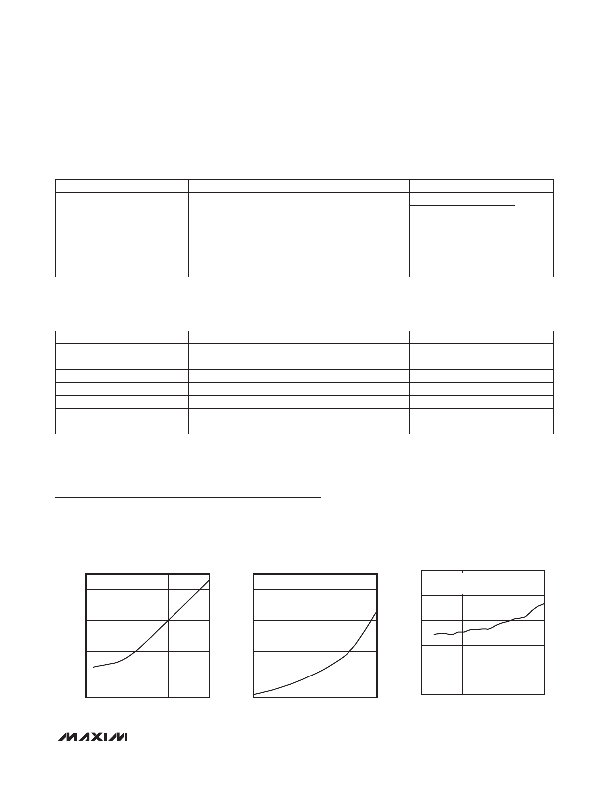
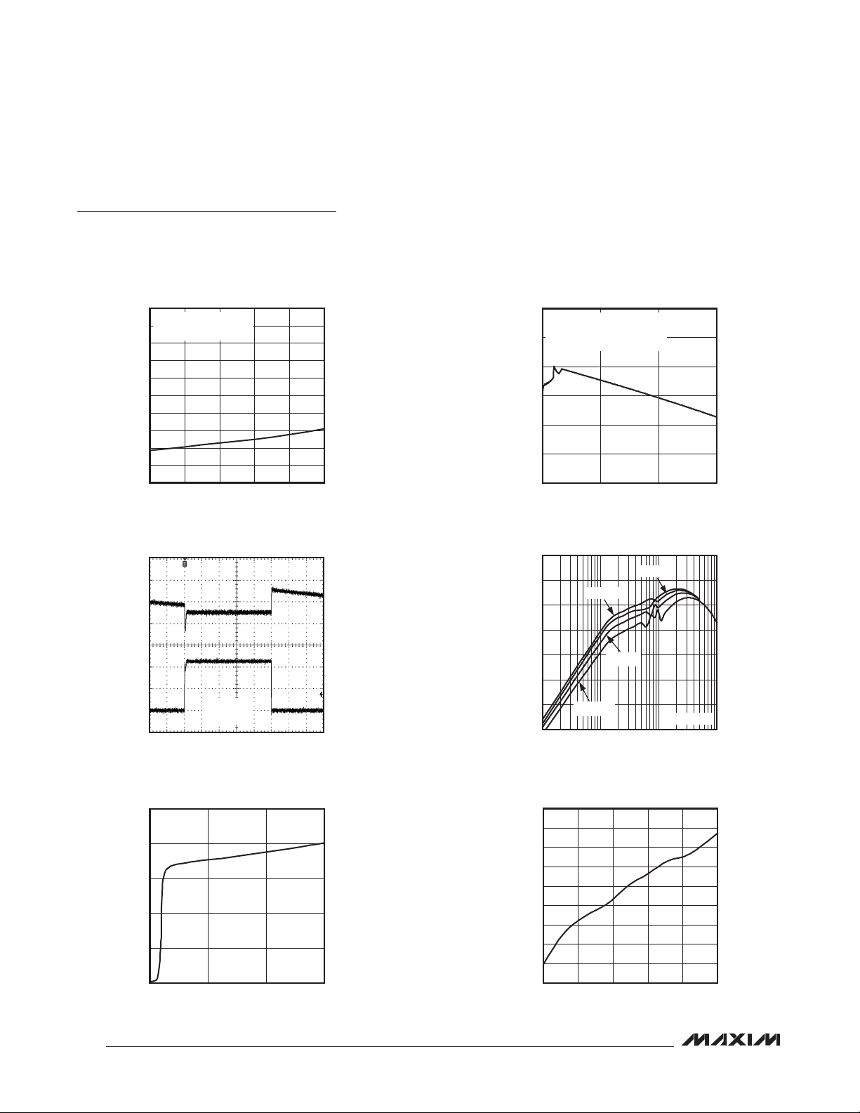
Typical Operating Characteristics
(MAX8982A: V
Circuits of Figures 2 and 3, unless otherwise noted. Typical values are at T
unless otherwise noted. Limits over the temperature range are guaranteed by design.
4.0
3.5
3.0
2.5
2.0
1.5
SHUTDOWN CURRENT (µA)
1.0
0.5
0
4.0 5.5
IN1A
= V
= 5V, MAX8982X: V
IN1B
SHUTDOWN CURRENT
vs. INPUT VOLTAGE (MAX8982A)
5.04.5
INPUT VOLTAGE (V)
= V
IN1A
4.0
3.5
MAX8982A toc01
3.0
2.5
2.0
1.5
SHUTDOWN CURRENT (µA)
1.0
0.5
0
3.0 5.5
IN1B
= V
DDA
= V
= V
DDB
= +25°C. Limits are 100% production tested at T
A
SHUTDOWN CURRENT
vs. INPUT VOLTAGE (MAX8982X)
5.04.53.5 4.0
INPUT VOLTAGE (V)
= 3.3V, C
IN4
)
REFBP
300
280
260
MAX8982A toc02
240
220
200
180
160
SHUTDOWN CURRENT (µA)
140
120
100
4.0 5.5
= 0.1µF, TA = -40°C to +85°C,
= +25NC,
A
NO LOAD SUPPLY CURRENT
vs. INPUT VOLTAGE (MAX8982A)
BUCK3, OUT3 ON
ALL OTHER OUTPUTS OFF
5.04.5
INPUT VOLTAGE (V)
19
MAX8982A toc03
Page 20
Power-Management ICs for
ICERA E400/E450 Platform
Typical Operating Characteristics (continued)
(MAX8982A: V
Circuits of Figures 2 and 3, unless otherwise noted. Typical values are at T
unless otherwise noted. Limits over the temperature range are guaranteed by design.
300
280
260
240
220
200
180
160
SHUTDOWN CURRENT (uA)
140
120
100
MAX8982A/MAX8982X
V
BUCK1
IN1A
= V
= 5V, MAX8982X: V
IN1B
NO LOAD SUPPLY CURRENT
vs. INPUT VOLTAGE (MAX8982X)
OUT3 ON
ALL OTHER OUTPUTS OFF
4.54.03.53.0 5.5
INPUT VOLTAGE (V)
BUCK1 LOAD TRANSIENT
5.0
MAX8982A toc06
= V
IN1A
MAX8982A toc04
AC-COUPLED
200mV/div
IN1B
= V
DDA
= V
= V
DDB
= +25°C. Limits are 100% production tested at T
A
= 3.3V, C
IN4
= 0.1µF, TA = -40°C to +85°C,
REFBP
)
BUCK1 LOAD REGULATION
0.950
L = 2.2µH, HITACHI METALS LTD
KSLI-252012AG-2R2
0.925
DCR = 100m
0.900
0.875
0.850
OUTPUT VOLTAGE (V)
0.825
0.800
0 1200
I
700200
LOAD CURRENT (mA)
BUCK1 EFFICIENCY
vs. LOAD CURRENT
100
V
= 4.5V
90
80
V
= 4.1V
IN
IN
A
MAX8982A toc05
MAX8982A toc07
= +25NC,
V
= 1V
I
BUCK1
OUT
C
OUT
= 10µF
100µs/div
BUCK1 SWITCHING FREQUENCY
vs. LOAD CURRENT
2.5
2.0
1.5
1.0
SWITCHING FREQUENCY (MHz)
0.5
0
0 1200
LOAD CURRENT (mA)
70
1.2A
1mA
60
EFFICIENCY (%)
50
40
30
1 1000
V
= 5V
IN
V
= 5.5V
IN
LOAD CURRENT (mA)
10010
V
= 0.9V
OUT
BUCK1 SWITCHING FREQUENCY
vs. TEMPERATURE
2.200
2.150
MAX8982A toc08
700200
2.100
2.050
2.000
1.950
1.900
1.850
SWITCHING FREQUENCY (MHz)
1.800
1.750
-40 85
TEMPERATURE (°C)
603510-15
MAX8982A toc09
20
Page 21
Power-Management ICs for
ICERA E400/E450 Platform
Typical Operating Characteristics (continued)
(MAX8982A: V
Circuits of Figures 2 and 3, unless otherwise noted. Typical values are at T
unless otherwise noted. Limits over the temperature range are guaranteed by design.
IN1A
= V
= 5V, MAX8982X: V
IN1B
IN1A
= V
IN1B
= V
DDA
= V
= V
DDB
= +25°C. Limits are 100% production tested at T
A
= 3.3V, C
IN4
= 0.1µF, TA = -40°C to +85°C,
REFBP
)
= +25NC,
A
MAX8982A/MAX8982X
BUCK1 RAMP-UP TRANSITION
V
BUCK1
NO LOAD
12.5mV/µs RAMP RATE
20µs/div
BUCK2 LOAD REGULATION
1.820
1.800
1.780
1.760
OUTPUT VOLTAGE (V)
1.740
L = 1.0µH, MURATA LQM2MPN1R0NG0
I
DCR = 85m
1.720
0 600
LOAD CURRENT (mA)
MAX8982A toc10
1.2V
0.6V
MAX8982A toc12
400200
V
BUCK1
V
BUCK2
I
BUCK2
BUCK1 RAMP-DOWN TRANSITION
I
= 1.2A
OUT
12.5mV/µs RAMP RATE
20µs/div
BUCK2 LOAD TRANSIENT
V
= 1.8V
OUT
40µs/div
MAX8982A toc11
MAX8982A toc13
1.2V
0.6V
AC-COUPLED
100mV/div
600mA
1mA
100
90
80
70
EFFICIENCY (%)
60
50
40
BUCK2 EFFICIENCY
vs. LOAD CURRENT
V
IN
V
= 4.1V
IN
V
= 5.5V
IN
100101 1000
LOAD CURRENT (mA)
= 4.5V
V
IN
= 5V
MAX8982A toc14
BUCK3 LOAD REGULATION
(MAX8982A ONLY)
3.300
L = 2.2µH, HITACHI METALS LTD
KSLI-252012AG-2R2
3.250
3.200
3.150
3.100
OUTPUT VOLTAGE (V)
3.050
3.000
0 600
DCR = 100m
I
LOAD CURRENT (mA)
MAX8982A toc15
500400300200100
21
Page 22

Power-Management ICs for
ICERA E400/E450 Platform
Typical Operating Characteristics (continued)
(MAX8982A: V
Circuits of Figures 2 and 3, unless otherwise noted. Typical values are at T
unless otherwise noted. Limits over the temperature range are guaranteed by design.
V
BUCK3
I
BUCK3
MAX8982A/MAX8982X
3.410
3.400
3.390
3.380
3.370
3.360
OUTPUT VOLTAGE (V)
3.350
3.340
3.330
IN1A
= V
= 5V, MAX8982X: V
IN1B
BUCK3 LOAD TRANSIENT
(MAX8982A ONLY)
20µs/div
V
OUT
C
OUT
MAX8982A toc16
= 3.2V
= 10µF
BUCK4 LOAD REGULATION
(MAX8982A ONLY)
L = TAIYO YUDEN NR3015T1R0N
I
DCR = 30m
0 600
LOAD CURRENT (mA)
500400100 200 300
= V
IN1A
AC-COUPLED
100mV/div
600mA
1mA
MAX8982A toc18
IN1B
= V
DDA
= V
= V
DDB
= +25°C. Limits are 100% production tested at T
A
= 3.3V, C
IN4
= 0.1µF, TA = -40°C to +85°C,
REFBP
)
BUCK3 EFFICIENCY
vs. LOAD CURRENT (MAX8982A ONLY)
100
EFFICIENCY (%)
V
= 4.1V
95
90
85
80
75
70
65
60
55
50
IN
V
= 5.5V
IN
1 1000
LOAD CURRENT (mA)
BUCK4 LOAD TRANSIENT (MAX8982A ONLY)
V
BUCK4
I
BUCK4
V
= 3.4V
OUT
1mA TO 1.5A
20µs/div
V
= 4.5V
IN
V
= 5V
IN
V
= 3.2V
OUT
10010
MAX8982A toc19
A
MAX8982A toc17
AC-COUPLED
50mV/div
1.5A
1mA
= +25NC,
22
BUCK4 EFFICIENCY vs. LOAD CURRENT
(MAX8982A ONLY)
100
90
80
70
60
50
EFFICIENCY (%)
40
30
20
10
1 10,000
LOAD CURRENT (mA)
VIN = 4.1V
VIN = 4.5V
VIN = 5V
VIN = 5.5V
BUCK4 SWITCHING FREQUENCY
vs. LOAD CURRENT (MAX8982A ONLY)
2.5
MAX8982A toc20
V
= 3.4V
OUT
100010010
2.0
1.5
1.0
SWITCHING FREQUENCY (MHz)
0.5
0
0 600
LOAD CURRENT (mA)
400200
MAX8982A toc21
Page 23

Power-Management ICs for
ICERA E400/E450 Platform
Typical Operating Characteristics (continued)
(MAX8982A: V
Circuits of Figures 2 and 3, unless otherwise noted. Typical values are at T
unless otherwise noted. Limits over the temperature range are guaranteed by design.
IN1A
= V
= 5V, MAX8982X: V
IN1B
IN1A
= V
IN1B
= V
DDA
= V
= V
DDB
= +25°C. Limits are 100% production tested at T
A
= 3.3V, C
IN4
= 0.1µF, TA = -40°C to +85°C,
REFBP
)
= +25NC,
A
MAX8982A/MAX8982X
BUCK4 SWITCHING FREQUENCY
vs. TEMPERATURE (MAX8982A ONLY)
2.20
2.15
2.10
2.05
2.00
1.95
1.90
SWITCHING FREQUENCY (MHz)
1.85
1.80
-40 85
TEMPERATURE (°C)
LDO3 LOAD REGULATION
2.820
2.815
2.810
2.805
2.800
OUTPUT VOLTAGE (V)
LDO1 LOAD REGULATION
2.705
2.704
MAX8982A toc22
2.703
2.702
2.701
2.700
OUTPUT VOLTAGE (V)
2.699
2.698
6035-15 10
2.697
0 300
LOAD CURRENT (mA)
25020050 100 150
1.812
1.810
1.808
MAX8982A toc23
1.806
1.804
1.802
1.800
1.798
OUTPUT VOLTAGE (V)
1.796
1.794
1.792
1.790
LDO2 LOAD REGULATION
0 150
LOAD CURRENT (mA)
10050
MAX8982A toc24
LDO4 LOAD REGULATION
0.903
MAX8982A toc25
0.902
OUTPUT VOLTAGE (V)
MAX8982A toc26
2.795
2.790
0 150
LOAD CURRENT (mA)
10050
LDO5 LOAD REGULATION
3.020
3.010
3.000
2.990
2.980
OUTPUT VOLTAGE (V)
2.970
2.960
0 150
LOAD CURRENT (mA)
10050
MAX8982A toc27
0.901
0 50
LOAD CURRENT (mA)
LDO6 LOAD REGULATION
2.720
2.715
2.710
2.705
2.700
OUTPUT VOLTAGE (V)
2.695
2.690
0 150
LOAD CURRENT (mA)
40302010
MAX8982A toc28
10050
23
Page 24

Power-Management ICs for
ICERA E400/E450 Platform
Typical Operating Characteristics (continued)
(MAX8982A: V
Circuits of Figures 2 and 3, unless otherwise noted. Typical values are at T
unless otherwise noted. Limits over the temperature range are guaranteed by design.
3.025
3.020
3.015
3.010
3.005
3.000
OUTPUT VOLTAGE (V)
2.995
2.990
2.985
MAX8982A/MAX8982X
0.902
IN1A
= V
= 5V, MAX8982X: V
IN1B
LDO7 LOAD REGULATION
0 100
LOAD CURRENT (mA)
806020 40
LDO9 LOAD REGULATION
IN1A
MAX8982A toc29
MAX8982A toc31
= V
IN1B
= V
DDA
= V
= V
DDB
= +25°C. Limits are 100% production tested at T
A
= 3.3V, C
IN4
= 0.1µF, TA = -40°C to +85°C,
REFBP
)
LDO8 LOAD REGULATION
(MAX8982A ONLY)
3.020
3.015
3.010
3.005
3.000
OUTPUT VOLTAGE (V)
2.995
2.990
2.985
0 100
LOAD CURRENT (mA)
80604020
LED CURRENT ACCURACY
vs. LED CURRENT SETTING
10
8
6
4
LUMEX SML-LX2832SISUGSBC
LED3
A
MAX8982A toc30
MAX8982A toc32
= +25NC,
24
OUTPUT VOLTAGE (V)
0.900
0 100
LOAD CURRENT (mA)
LED FLASH WAVEFORMS
I
LED2
I
LED3
1s/div
80604020
MAX8982A toc33
24mA
0A
24mA
0A
2
0
LED CURRENT ACCURACY (%)
-2
-4
0 25
LED CURRENT (mA)
OVERVOLTAGE PROTECTION
V
IN_
V
BUCK1
V
BUCK2
V
LDO1
400µs/div
LED2
2015105
MAX8982A toc34
5V/div
0V
1V/div
0V
1V/div
0V
2V/div
0V
Page 25

Power-Management ICs for
ICERA E400/E450 Platform
Pin Configurations
TOP VIEW
(BUMP ON BOTTOM)
1 2 3 4 5 6 7
MAX8982A
MAX8982A/MAX8982X
N32
A
kHz
B
OUT4 DR1 DR2 OUT8 VSIM
C
IN3 DR3
LX2
D
PGND2
E
F
PGND1
OUT9 GND
RESET IRQ
BUCK2
BUCK1
LX1 IN4 IN1A
DVS1 SDA
EN IN1B LX4
OUT5
WLP
REF
BP
OUT6 OUT2
SCL OUT1
PWR_
REQ
LX4
OUT3
V
DDB
BUCK3
BUCK4
PGND4 PGND4
V
LX3
PGND3
DDA
25
Page 26

Power-Management ICs for
ICERA E400/E450 Platform
Pin Configurations (continued)
TOP VIEW
(BUMP ON BOTTOM)
1 2 3 4 5 6 7
MAX8982X
N32
A
kHz
B
OUT4 DR1 DR2 DNC
C
IN3 DR3
OUT9 GND
RESET IRQ
MAX8982A/MAX8982X
LX2
D
PGND2 PGND3
E
F
PGND1
BUCK2
BUCK1
LX1 IN4 IN1A
DVS1 SDA
EN IN1B DNC DNC
REF
BP
OUT5
WLP
OUT6 OUT2
VSIM
SCL OUT1
PWR_
REQ
DNC
OUT3
V
DDB
DNC DNC
PGND4 PGND4
V
DDA
26
Page 27

Power-Management ICs for
ICERA E400/E450 Platform
Pin Description
MAX8982A/MAX8982X
PIN
GROUND
A3 GND GND Analog Ground
F1 PGND1 PGND1 Power Ground for BUCK1
E1 PGND2 PGND2 Power Ground for BUCK2
E7 PGND3 PGND3 Power Ground for BUCK3
F6, F7 PGND4 PGND4 Power Ground for BUCK4
INPUT SUPPLY
F4
E4 IN1B IN1B Input Supply to the IC. Connect IN1B to IN1A.
C1 IN3 IN3
F3
B7
B6
BUCK CONVERTERS
F2 LX1 LX1
D1 LX2 LX2
D7
E5, F5
E2 BUCK1 BUCK1 BUCK1 Output Feedback
D2 BUCK2 BUCK2 BUCK2 Output Feedback
D6
E6
MAX8982A MAX8982X
NAME
Input Supply to the IC. The operating voltage range for the MAX8982A is 4.1V to 5.5V.
IN1A —
— IN1A
IN4 —
— IN4 Connect IN4 to Both IN1A and IN1B
V
DDA
— V
V
DDB
— V
LX3 —
— DNC Do Not Connect
LX4 —
— DNC Do Not Connect
BUCK3 — BUCK3 Output Feedback
— DNC Do Not Connect
BUCK4 — BUCK4 Output Feedback
— DNC Do Not Connect
—
DDA
— Power Input for LDO3, LDO5, LDO6, and LDO7. Connect V
DDB
Connect three 330FF tantalum capacitors as close as possible to IN1A and IN1B.
Connect IN1A to IN1B.
Input Supply to the IC. The operating voltage range for the MAX8982X is 2.9V to 5.5V.
Bypass with a 22FF ceramic capacitor as close as possible to IN1A and IN1B. Connect
IN1A to IN1B.
Input Supply for LDO4 and LDO9. Connect IN3 to the BUCK2 output. Bypass IN3 with a
2.2FF ceramic capacitor as close as possible to IN3.
Input Supply for LDO8. Bypass with a 1FF ceramic capacitor as close as possible to IN4.
The IN4 operating range is from 3.0V to 5.5V. Connect IN4 to either IN1A and IN1B.
Power Input for LDO1 and LDO2. Connect V
ceramic capacitor as close as possible to V
Power Input for LDO1 and LDO2. Connect V
Power Input for LDO3, LDO5, LDO6, and LDO7. Connect V
BUCK1 Inductor Connection. LX1 connects to the drains of the internal p-channel and
n-channel MOSFETs.
BUCK2 Inductor Connection. LX2 connects to the drains of the internal p-channel and
n-channel MOSFETs.
BUCK3 Inductor Connection. LX3 connects to the drains of the internal p-channel and
n-channel MOSFETs.
BUCK4 Inductor Connection. LX4 connects to the drains of the internal p-channel and
n-channel MOSFETs. Connect the two LX4 bumps together externally.
FUNCTION
DDA
.
DDA
DDA
to V
to V
. Bypass V
DDB
, IN1A, and IN1B.
DDB
to V
DDB
to V
DDB
with a 10FF
DDA
.
DDA
IN1A, and IN1B
DDA,
.
27
Page 28

Power-Management ICs for
ICERA E400/E450 Platform
Pin Description (continued)
PIN
LDO REGULATORS
C7 OUT1 OUT1
A7 OUT2 OUT2
A6 OUT3 OUT3
B1 OUT4 OUT4
C4 OUT5 OUT5
A5 OUT6 OUT6
MAX8982A/MAX8982X
B5 VSIM VSIM
B4
A2 OUT9 OUT9
2
I
C INTERFACE
D4 SDA SDA I
C5 SCL SCL I
CURRENT REGULATORS
B2 DR1 DR1
B3 DR2 DR2
C2 DR3 DR3
LOGIC INPUTS
E3 EN EN Active-High IC Enable Input
D5 PWR_REQ PWR_REQ
D3 DVS1 DVS1 BUCK1 Output Selection Input for DVS Function
MAX8982A MAX8982X
NAME
LDO1 Output. Bypass OUT1 with a 4.7FF ceramic capacitor. OUT1 supplies loads up to
300mA. The default output voltage is 2.7V.
LDO2 Output. Bypass OUT2 with a 1FF ceramic capacitor. OUT2 supplies loads up to
150mA. The default output voltage is 1.8V.
LDO3 Output. Bypass OUT3 with a 1FF ceramic capacitor. OUT3 supplies loads up to
150mA. The default output voltage is 2.8V.
LDO4 Output. Bypass OUT4 with a 2.2FF ceramic capacitor. OUT4 supplies loads up to
50mA. The default output voltage is 0.9V.
LDO5 Output. Bypass OUT5 with a 1FF ceramic capacitor. OUT5 supplies loads up to
150mA. The default output voltage is 3.0V.
LDO6 Output. Bypass OUT6 with a 1FF ceramic capacitor. OUT6 supplies loads up to
150mA. The default output voltage is 2.7V.
LDO7 Output. Bypass VSIM with a 1FF ceramic capacitor. VSIM supplies loads up to
150mA. The default output voltage is 3V.
OUT8 —
— DNC Do Not Connect
LDO8 Output. Bypass OUT8 with a 1FF ceramic capacitor. OUT8 supplies loads up to
150mA. The default output voltage is 3V.
LDO9 Output. Bypass OUT9 with a 2.2FF ceramic capacitor. OUT9 supplies loads up to
50mA. The default output voltage is 0.9V.
2
C Data. SDA is high impedance when off.
2
C Clock. SCL is high impedance when off.
Current Regulated Driver 1. Typically used to drive an LED. DR1 can be programmed to
sink 3mA to 24mA in 8 steps (24mA default). If the flash timer is activated, the LED can
be programmed to turn on/off in a preprogrammed pattern. See the Embedded Flash
Timer section.
Current Regulated Driver 2. Typically used to drive an LED. DR2 can be programmed to
sink 3mA to 24mA in 8 steps (24mA default). If the flash timer is activated, the LED can
be programmed to turn on/off in a preprogrammed pattern. See the Embedded Flash
Timer section.
Current Regulated Driver 3. Typically used to drive an LED. DR3 can be programmed to
sink 3mA to 24mA in 8 steps (24mA default). If the flash timer is activated, the LED can
be programmed to turn on/off in a preprogrammed pattern. See the Embedded Flash
Timer section.
Active-High to Enable All Designated Step-Down Regulators and LDOs in Sequence.
Active-high/low to enable/disable all step-down converters and LDOs after power-on. The
values in the BUCK1DVS1 and BUCK1DVS2 registers are reset to their defaults when
PWR_REQ goes low in normal operation.
FUNCTION
28
Page 29

Power-Management ICs for
ICERA E400/E450 Platform
Pin Description (continued)
MAX8982A/MAX8982X
PIN
LOGIC OUTPUTS
C6 IRQ IRQ Active-Low, Open-Drain Interrupt Output. Internal pullup resistor, 200kI, to BUCK2.
C3 RESET RESET Active-Low, Open-Drain Reset Output. There is an internal 14kI pullup resistor to BUCK2.
REFERENCE OUTPUT
A4 REFBP REFBP
32kHz CLOCK
A1 N32kHz N32kHz 32kHz Clock Output. This output is supplied from BUCK2.
MAX8982A MAX8982X
NAME
FUNCTION
Reference Bypass. Connect the reference bypass capacitor from REFBP to GND. See
Table 3. High impedance in off condition. V
power to external circuitry.
is 0.8V (typ). Do not use to provide
REFBP
Table 1. Summary of Power Supplies
PARAMETER BUCK1 BUCK2 BUCK3* BUCK4* OUT1 OUT2 OUT3 OUT4 OUT5 OUT6
Function Core
Default
Voltage (V)
Continuous
Output Current
(mA)
Programmable
Voltage
Options (V)
0.9 1.8 3.2 3.4 2.7 1.8 2.8 0.9 3.0 2.7 3.00
1200 600 600 1800 300 150 150 50 150 150 150
0.600 N/A 2.90 3.00 2.65 1.5 2.65 0.8 2.80 2.65 1.80
25mV
step
1.20
SystemIOLDO
INPUT
2.95 3.05 2.70 1.8 2.70 0.9 2.90 2.70 3.00
3.00 3.10 2.75 2.7 2.75 1.0 3.00 2.75
3.05 3.15 2.80 1.7 2.80 1.1 3.20 2.80
3.10 3.20 2.85 2.85 1.2 2.85
3.15 3.25 2.90 2.90 2.90
3.20 3.30 2.95 2.95 2.95
3.25 3.35 3.00 3.00 3.00
3.30 3.40
3.35 3.45
3.40 3.50
3.45 3.55
3.50 3.60
3.55 3.65
3.60 3.70
3.65 3.75
PA RF RF Analog PLL SD TCXO SIM
OUT7
(VSIM)
OUT8* OUT9
USB BB
3.0 0.9
150 50
3.00 0.8
3.10 0.9
3.20 1.0
3.30 1.1
1.2
*BUCK3, BUCK4, and OUT8 are for the MAX8982A only.
29
Page 30

Power-Management ICs for
ICERA E400/E450 Platform
Table 1. Summary of Power Supplies (continued)
PARAMETER BUCK1 BUCK2 BUCK3* BUCK4* OUT1 OUT2 OUT3 OUT4 OUT5 OUT6
Default ON
at Initial
Startup
ON/OFF
Control After
Power-Up
Default
Active
Discharge
Resistor
*BUCK3, BUCK4, and OUT8 are for the MAX8982A only.
PWR_
REQ
2
C
I
or
PWR_
REQ
OFF ON OFF OFF OFF OFF OFF OFF OFF OFF OFF
ON ON
I2C
or
PWR_
REQ
I2C
or
PWR_
REQ
OFF
I2C
or
PWR_
REQ
PWR_
REQ
I2C
or
PWR_
REQ
PWR_
REQ
I2C
or
PWR_
REQ
PWR_
REQ
ON
I2C
or
PWR_
REQ
I2C
or
PWR_
REQ
OFF
I2C
or
PWR_
REQ
MAX8982A/MAX8982X
PWR_
REQ
I2C
or
PWR_
REQ
OUT7
(VSIM)
OFF
I2C
or
PWR_
REQ
OUT8* OUT9
ON
ON
2
I
C
I2C
or
PWR_
REQ
OFF OFF
or
PWR_
REQ
30
Page 31

Power-Management ICs for
ICERA E400/E450 Platform
MAX8982A/MAX8982X
INPUT
USB
5V
DD+
G
IN1_
0.1µF
BB
TCXO
BB
CHIPSET
ICE8060
ON E400
PLATFORM
INTERRUPT
3.0V
HS USB
TRANSCEIVER
BB
OSC 32kI
PWR_REQ
(1.2A)
LDO4
(50mA)
RESET
LDO3
150mA
LDO2
LDO1
LDO5
150mA
625µs
INPUT
IN1A
LX4
P
LX4
N
PGND4
PGND4
P
N
P
N
N
BUCK2
14kI
P
N
N
N
N
N
N
BUCK4
LX1
PGND1
BUCK1
DVS1
LX2
PGND2
BUCK2
IN3
OUT4
2.2µF
RESET
LX3
PGND3
BUCK3
VDDA
VDDB
OUT3
1µF
OUT2
1µF
OUT1 2.7V
4.7µF
OUT5
1µF
VSIM
1µF
IN1A
IN1A
IN1A
LDO
2.2µH
3.0V TO 3.75V IN 50mV STEPS
0.9V (DEFAULT)
2.2µH
IN 25mV STEPS
1µH
2.2µF
3.2V (DEFAULT)
2.9V TO 3.65V
2.2µH
IN 50mV STEPS
3.4V (DEFAULT)
0.6V TO 1.2V
0.9V
10µF
2.8V
1.8V
3.0V
2.2µF
2.2µF
2.2µF
1.8V
2.2µF
CORE
DCDC 1 SEL
VCC_IO
PLL
BB CHIPSET
ICE 8060
ON E400
PLATFORM
POR_N
RTBON
ANALOG
BASEBAND
RF1V8
CHIPSET
ICE 8260
RF2V7
SD CARD
USIM
GSM PA/
UMTS PA
RF
IN1A
IN1B
330µF * 3
REFBP
GND
OUT9
0.9V
2.2µF
N
2.7V
OUT6
1µF
N
IN1_
SDA
SCL
IN1_
1µF
1µF
IN1_
PWR_REQ
OPTIONAL
RESISTORS
EN
200kI
IRQ
SDA
SCL
IN4
OUT8
N
N32kHz
DR1
DR2
DR3
3.8V
5.75V
(50mA)
(50mA)
ON/OFF
SEQUENCE
SHUTDOWN
SIGNAL
BUCK2
(DEFAULT ON)
150mA
OSCILLATOR
BUCK2
3-CHANNEL
CURRENT
REGULATOR
(24mA,
DEFAULT)
(3—24mA IN 3mA STEPS)
LDO9
LDO6
LDO8
32kHz
UVLO
OVP
TIMER
FLASH
TIMER
16ms
ON/OFF SEQUENCE
SHUTDOWN SIGNAL
IN3
V
DDB
REF
IN1B
UVLO
(3.8V)
THERMAL
SHUTDOWN
+160°C
ON/OFF CONTROL
AND
2
C INTERFACE
I
MAX8982A
(0.8V)
STEP-DOWN
CONVERTER 4
(1.8A)
STEP-DOWN
DC-DC 1
BUCK2
V
DDB
V
DDA
V
DDA
V
DDB
V
DDB
CONVERTER
STEP-DOWN
DC-DC 2
CONVERTER
(DEFAULT
ON, 600mA)
STEP-DOWN
DC-DC 3
CONVERTER
(DEFAULT ON)
DEFAULT ON
(150mA)
(300mA)
(150mA)
1.8V/3.0V
SIM LDO (LDO7)
REF
Figure 1. MAX8982A Typical Application Circuit and Functional Block Diagram
31
Page 32

Power-Management ICs for
ICERA E400/E450 Platform
Table 2. External Component List for Figure 1
LOCATION EXTERNAL COMPONENTS NOTES
IN1A, IN1B
IN3 2.2FF Input for LDO4 and LDO9
IN4 1.0FF Input for LDO8
OUT1 4.7FF
OUT2 1.0FF LDO compensation
OUT3 1.0FF LDO compensation
OUT4 2.2FF LDO compensation
OUT5 1.0FF LDO compensation
OUT6 1.0FF LDO compensation
VSIM (OUT7) 1.0FF LDO compensation
OUT8 1.0FF LDO compensation
OUT9 2.2FF LDO compensation
, V
V
DDA
MAX8982A/MAX8982X
BUCK1 for BB Core 2.2FF For low noise, 1.2A continuous load
BUCK2 for BB System IO 2.2FF For low noise
BUCK3 as LDO Input 2.2FF For low noise
DDB
3 x 330FF tantalum capacitors
Total capacitance R total output capacitance
for LDO1, LDO2, LDO3, LDO5, LDO6, and
VSIM. Use a 10FF capacitor on V
as recommended.
DDA/VDDB
Buck stability and GSM PA supply
LDO compensation and load transient
response
All LDOs stability
BUCK4 for GSM PA/UMTS PA 2 x 22FF Supply for both GSM PA and UMTS PA
LX1 1FH to 4.7FH 2.2FH recommended (Table 60)
LX2 1FH to 4.7FH 1.0FH recommended (Table 60)
LX3 1FH to 4.7FH 2.2FH recommended (Table 60)
LX4 1FH to 4.7FH 2.2FH recommended (Table 60)
REFBP 0.1FF Noise filter
EN A pulldown resistor, if necessary.
Any Bump Required to Pass 8kV
Module Level ESD
Note: Input/output capacitance should be as close as possible to the IC. All capacitors are ceramic X5R or X7R, unless otherwise noted.
0.1FF Absorb ESD energy
32
Page 33

Power-Management ICs for
ICERA E400/E450 Platform
MAX8982A/MAX8982X
0.1µF
VCC_USB
CHIPSET
ICE8060
ON E400
PLATFORM
OSC 32kI
TCXO
BB
INTERRUPT
PWR_REQ
BB
SDA
SCL
3.3V
INPUT
22µF
0.9V
2.2µF
2.7V
1µF
IN1_
3.3V INPUT
PWR_REQ
OPTIONAL
RESISTORS
V
V
IN1A
IN1B
REFBP
GND
OUT9
OUT6
N32kHz
IN1A
DDB
DDA
5.75V
IN4
EN
IRQ
SDA
SCL
2.7V
N
N
ON/OFF
SEQUENCE
SHUTDOWN
SIGNAL
BUCK2
200kI
LDO9
(50mA)
LDO6
(50mA)
16ms
TIMER
OVP
UVLO
IN3
V
DDB
SHUTDOWN SIGNAL
ON/OFF SEQUENCE
IN1B
UVLO
(2.7V)
ON/OFF CONTROL
AND
I2C INTERFACE
(0.8V)
THERMAL
SHUTDOWN
+160°C
STEP-DOWN
DC-DC 1
CONVERTER
(1.2A)
STEP-DOWN
DC-DC 2
CONVERTER
(DEFAULT
REF
ON, 600mA)
LDO4
(50mA)
ON = BUCK 2EN + 625µs
RESET
V
DDB
LDO3
DEFAULT ON
150mA
V
DDA
LDO2
(150mA)
MAX8982X
V
DDA
V
DDB
V
DDB
LDO1
(300mA)
LDO5
(150mA)
1.8V/3.0V
SIM LDO (LDO7)
150mA
32kHz
OSCILLATOR
BUCK2
DR1
DR2
DR3
3-CHANNEL
CURRENT
REGULATOR
(24mA,
DEFAULT)
(3—24mA IN 3mA STEPS)
FLASH
TIMER
IN1A
P
N
P
N
N
N
N
N
N
N
LX1
PGND1
BUCK1
DVS1
LX2
PGND2
BUCK2
IN3
OUT4
BUCK2
14kI
RESET
OUT3
OUT2
OUT1 2.7V
OUT5
V
SIM
4.7µF
0.9V (DEFAULT)
0.6V TO 1.2V
2.2µH
IN 25mV STEPS
1µH
2.2µF
1µF
1µF
1µF
1µF
1µF
CORE
2.2µF
DCDC 1 SEL
1.8V
VCC_IO
2.2µF
0.9V
VCC_PLL
BB CHIPSET
ICE 8060
ON E400
PLATFORM
POR_N
RTBON
ANALOG
2.8V
BASEBAND
1.8V
RF1V8
RF
CHIPSET
ICE 82 xx
RF2V7
3.0V
SD CARD
1.8V
USIM
Figure 2. MAX8982X Typical Application Circuit and Functional Block Diagram
33
Page 34

Power-Management ICs for
ICERA E400/E450 Platform
Table 3. External Component List for Figure 2
LOCATION EXTERNAL COMPONENTS NOTES
IN1A, IN1B
IN3 2.2FF Input for LDO4 and LDO9
IN4 Connect to IN1A and IN1B
OUT1 4.7FF
OUT2 1.0FF LDO compensation
OUT3 1.0FF LDO compensation
OUT4 2.2FF LDO compensation
OUT5 1.0FF LDO compensation
OUT6 1.0FF LDO compensation
VSIM (OUT7) 1.0FF LDO compensation
OUT9 2.2FF LDO compensation
, V
V
DDA
DDB
MAX8982A/MAX8982X
BUCK1 for BB Core 2.2FF For low noise, 1.2A continuous load
BUCK2 for BB System IO 2.2FF For low noise
LX1 1FH to 4.7FH 2.2FH recommended (Table 60)
LX2 1FH to 4.7FH 1.0FH recommended (Table 60)
REFBP 0.1FF Noise filter
EN A pulldown resistor, if necessary
Any Bump Required to Pass 8kV
Module Level ESD
Note: Input/output capacitance should be as close as possible to the IC. All capacitors are ceramic X5R or X7R, unless otherwise noted.
22FF
Total capacitance R total output capacitance
for LDO1, LDO2, LDO3, LDO5, LDO6, and
VSIM.
0.1FF Absorb ESD energy
Buck stability
LDO compensation and load transient
response
All LDOs stability. Connect V
V
to IN1A and IN1B.
DDB
DDA
and
Detailed Description
Power-On/Off Control
The power-on/off state diagram is shown in Figure 3.
When the IN1_ supply voltage is valid and EN is high,
the default power supplies turn on in sequence (Figure
4). Once powered up, any step-down or LDO output can
be enabled or disabled through I
grammed to be controlled by the PWR_REQ logic input.
PWR_REQ is a control input from baseband chipset used
to enable/disable specified regulators.
After power-up, when PWR_REQ goes logic-high, any
step-down or LDO output programmed for PWR_REQ
control is enabled in a predefined sequence. The regulators
are powered up in four groups as shown in Figure 5. See the
following for the regulators belonging to each group. When
PWR_REQ goes logic-low, all regulators programmed for
PWR_REQ control are turned off simultaneously.
34
2
C, or they can be pro-
PWR_REQ
2
Any regulator that is set to on or off though I
C is not
affected by PWR_REQ, except for BUCK1. The programmed values in BUCK1DVS1 and BUCK1DVS2 are
reset to their defaults when PWR_REQ goes low even in
normal operation.
Group A: BUCK3 (MAX8982A only)
LDO2 (default is PWR_REQ On mode)
BUCK2
Group B: LDO1 (default is PWR_REQ On mode)
LDO3
BUCK4 (MAX8982A only)
Group C: LDO6 (default is PWR_REQ On mode)
LDO5
LDO7
LDO8 (MAX8982A only)
Group D: BUCK1 (default is PWR_REQ On mode)
LDO4 (default is PWR_REQ On mode)
LDO9
Page 35

Power-Management ICs for
ICERA E400/E450 Platform
Active Discharge
All regulators include an internal resistor for discharging
the output when the regulator is shut down. In the default
state (except BUCK2), this resistor is not connected so
the output decay depends only on the applied load. To
V
< 3.5V (MAX8982A)
IN1_
< 2.4V (MAX8982X)
OR V
IN1_
> 5.75V
OR V
SHUTDOWN
ALL REGULATORS
DISABLED
2
I
C HIGH IMPEDANCE
REF DISABLED
32kHz DISABLED
V
V
AND EN = HIGH
POWER-UP
BUCK3 ENABLED (MAX8982A)
BUCK2 ENABLED
LDO3 ENABLED
LDO8 ENABLED (MAX8982A)
LDO9 ENABLED
RESET = HIGH
= 0.8V
V
REFBP
I2C ENABLED
32kHz CLOCK ENABLED
IN1_
IN1_
IN1_
OR EN = LOW
> 3.8V (TYP) (MAX8982A)
> 2.7V (TYP) (MAX8982X)
PWR_REQ = HIGH
enable this discharge resistor, set the appropriate bit in
the BUCK1-4ADIS, LDO1-8ADIS, or LDO9ADIS register.
The active discharge resistor values are specified in the
General Electrical Characteristics table.
FROM
ANY STATE
NOTE: ENABLE OF BUCKS AND
LDOS AND CONTROL OF
BUCKS AND LDOS
BY PWR_REQ
CAN BE MODIFIED
AFTER STARTUP THROUGH I
BUCK1 ENABLED
LDO1 ENABLED
LDO2 ENABLED
LDO4 ENABLED
LDO6 ENABLED
RESET = HIGH
V
= 0.8V
REFBP
I2C ENABLE
32kHz CLOCK ENABLED
2
C.
MAX8982A/MAX8982X
PWR_REQ
= HIGH
BUCK1 DISABLED
LDO1 DISABLED
LDO2 DISABLED
LDO4 DISABLED
LDO6 DISABLED
RESET = HIGH
V
= 0.8V
REFBP
I2C ENABLED
32kHz CLOCK ENABLED
PWR_REQ
= LOW
Figure 3. Power-On/Off State Diagram with IN3 Connected to BUCK2 Output and IN4 Connected to IN1_. Default PWR_REQ Regulators Are Shown.
35
Page 36

Power-Management ICs for
ICERA E400/E450 Platform
EN AND IN1_
BUCK 3
(3.2V)
BUCK 2
FOR IO (1.8V)
UVLO RISING
~16ms
UVLO FALLING
125µs
225µs
ON SEQUENCING RESTARTS
WHEN INPUT IS ABOVE
UVLO RISING
THRESHOLD
32kHz OUTPUT
OUT 3
FOR ANALOG (2.8V)
MAX8982A/MAX8982X
OUT 8
FOR USB (3.0V)
OUT 9
FOR BB (0.9V)
RESET
IRQ
OPERATING
STATE
OFF OFF
POWER-ON
SEQUENCE
375µs
125µs
125µs
625µs
CONTINUOUS
ON
OTHER ONREGULATORS
31µs TO 62µs
31µs
POWER-ON
SEQUENCE
Figure 4. MAX8982A/MAX8982X Power-On Timing Diagram at Initial Startup with EN Connected to IN1_. BUCK3 and OUT8 Are for the MAX8982A Only.
36
Page 37

PWR_REQ
Power-Management ICs for
ICERA E400/E450 Platform
MAX8982A/MAX8982X
GROUP A : OUT 2,*
BUCK 2, BUCK 3**
GROUP B : LDO1,*
OUT 3, BUCK 4**
GROUP C : OUT6,*
OUT5, OUT7, OUT8**
GROUP D : BUCK 1*, OUT4,*
OUT9
*THESE REGULATORS DEFAULT TO PWR_REQ CONTROL. THE OTHERS MUST BE PROGRAMED TO PWR_REQ CONTROL BY I
**BUCK3, BUCK4, AND OUT8 ARE FOR THE MAX8982A ONLY.
(BUILT-IN TIME DELAY TO
~10µs
ENABLE REGULATORS)
100µs
200µs
375µs
OUTPUT DECAY DEPENDS ON THE LOAD
2
C.
Figure 5. MAX8982A/MAX8982X Power-On Timing Diagram in PWR_REQ ON Mode After Power-Up
BUCK1, BUCK2, and BUCK3
Step-Down Converters
The step-down converters are optimized for high efficiency over a wide load range, small external component
size, low output ripple, and excellent transient response.
The step-down converters also feature an internal
MOSFET switch with optimized on-resistance and an
internal synchronous rectifier to maximize the efficiency
and reduce the number of external components. The ICs
use a proprietary hysteretic PWM control scheme that
switches with a nearly fixed frequency. Figure 6 shows
the frequency variation versus load current with a 5V
input supply and at T
= +25°C.
A
The default output is 0.9V. The BUCK1 voltage is programmable through I
BUCK1 includes DVS that allows two output voltages
to be programmed through I
trol input to select between the two voltages. Toggling
DVS1 changes the BUCK1 output voltage on-the-fly
between the two programmed voltages (Figure 7). Each
BUCK1DVS_ register specifies a voltage in the 0.6V to
1.2V range in 25mV increments.
Setting the Output Voltage on BUCK1
2
C from 0.6V to 1.2V in 25mV increments.
Dynamic Voltage Scaling (DVS)
Function on Buck 1
2
C, and an external con-
FREQUENCY vs. LOAD AT 5V INPUT
2.8
2.6
2.4
2.2
2.0
1.8
1.6
1.4
1.2
1.0
FREQUENCY (MHz)
0.8
0.6
0.4
0.2
0
1 10 50 100 200 300 400 500
LOAD (mA)
BUCK1
BUCK2
BUCK3
Figure 6. Frequency Variation vs. Load Current with a 5V Input Supply
BUCK1DVS1
(0X3F)
I2C INTERFACE
0.6V TO 1.2V
IN 25mV STEPS
(DEFAULT = 0.9V)
BUCK1DVS2
(0X40)
(DEFAULT = 0.9V)
TRUTH TABLE
DVS1 BUCK1 OUTPUT
High Set by BUCK1DVS2 register
Low Set by BUCK1DVS1 register
Figure 7. DVS1 Logic Diagram
BUCK1 OUTPUT
(DEFAULT = 0.9V)
DVS1
37
Page 38

Power-Management ICs for
ICERA E400/E450 Platform
Ramp-Up/Down Slope Control on BUCK1
BUCK1 uses a controlled ramp rate when it is enabled
and when changing between output voltage settings.
Four programmable slew rates are available for BUCK1.
The default value is 12.5mV/Fs (Table 4). The same slew
rate is applied for ramp-up/down.
Setting the Output Voltage on BUCK2
The BUCK2 output voltage is fixed at 1.8V. No programmable output is available.
Setting the Output Voltage on BUCK3
The BUCK3 default output is 3.2V. The BUCK3 output
voltage is programmable from 2.9V to 3.65V in 50mV
increments through I
MAX8982A.
2
C. BUCK3 is only available on the
BUCK4 Step-Down Converter
for PA (Power Amplifier)
BUCK4 is a 2MHz fixed-frequency PWM step-down
converter, typically used to supply the power amplifier
MAX8982A/MAX8982X
(PA). The BUCK4 load capability is 1.8A. BUCK4 is only
available on the MAX8982A.
Setting the Output Voltage on BUCK4
The default output voltage is 3.4V. The BUCK4 output
voltage is programmable between 3.0V and 3.75V in
50mV increments through I
2
C.
Linear Regulators
All linear regulators are designed for low-drop, low noise,
high PSRR, and low quiescent current to minimize power
consumption. If the input voltage is above UVLO threshold and power-on is logic-high, the default linear regulator (LDO3) turns on. The other LDOs are turned on and
off by the baseband processor through the I
or PWR_REQ control signal. All LDO output voltages are
programmable through the I
voltages.
2
C interface within option
2
C interface
Reference Bypass (REFBP)
The reference bypass is for low noise filtering only and
must not be loaded. Bypass REFBP with a 0.1FF ceramic
capacitor. The REFBP voltage is 0.8V (typ). Do not use
REFBP to provide power to external circuitry.
Thermal Overload Protection
If the internal die temperature of any LDOs or stepdown regulators reaches +160NC, the ICs shut down the
regulator locally. The regulator is reenabled after it cools
by 10NC. The ICs also contain a single +125NC thermal
detector located in the center of the die. When the temperature at the center of the die exceeds +125NC, this
detector triggers and activates an interrupt.
Undervoltage Lockout (UVLO)
The ICs monitor the voltage at the IN1_ power input.
When this voltage drops below 3.5V (MAX8982A) or
2.4V (MAX8982X), the ICs shut down. The ICs turn on
when this voltage rises above 3.8V (MAX8982A) or 2.7V
(MAX8982X) and EN is high. After a UVLO event, all registers are reset to their POR value.
Overvoltage Protection (OVP)
If the voltage on the IN1_ or IN4 inputs exceeds 5.75V
(typ), the ICs shut down. When the supply voltage
returns to within the valid operating range and EN is
high, the ICs turn on and go through a normal power-up
sequence. All registers are reset to their default poweron reset (POR) value.
Power-On Reset (POR)
Power-on reset (POR) for I2C occurs when the ICs turn
off due to UVLO, OVP, or EN = low. This condition puts
the IC into shutdown and then clears all previously programmed output voltages in the internal registers.
The programmed values in BUCK1DVS1 and
BUCK1DVS2 are also reset to their defaults when
PWR_REQ goes low in normal operation mode.
Table 4. BUCK1 Ramp-Up/Down Slope Control Settings
RASD1[1] RASD1[0] SLEW RATE (mV/µs)
0 0 5
0 1 10
1 0 12.5 (default)
1 1 25
38
V
BUCK1
Figure 8. BUCK1 Ramp-Up/Down Slope Control
UP SLOPE
CONTROL
DOWN
SLOPE
CONTROL
Page 39

Power-Management ICs for
POR ON ALL REGISTERS
IN MAX8982A/
MAX8982X
ICERA E400/E450 Platform
MAX8982A/MAX8982X
EN = LOW
OR
IN1_ INVALID
2
I
C ENABLED
Figure 9. POR State Diagram
Current Regulators (DR1, DR2, DR3)
The ICs have three current regulators that can handle
up to 24mA. The sink current for each current regulator
2
is set from 3mA to 24mA in 3mA increments through I
C.
The default set current is 24mA on each channel.
If a current other than the programmable options is
required, a series resistor can be added to set a current
from 0mA to 24mA (Figure 10). The resistor forces the
current regulator to operate in dropout. Set the resistor
value to (V
IN1_
- VF)/I
age of the LED at the desired current and I
desired LED current. I
, where VF is the forward volt-
LED
LED
must be less than the pro-
LED
is the
grammed current (24mA default).
Each current regulator has an embedded flash timer.
2
The flash time is programmable through the I
C interface. This feature allows the system designer to generate
a desired pattern on LED.
Embedded Flash Timer
The flash generator is clocked by the internal 32kHz oscillator. It consists of a counter that wraps at a programmable
value to provide a configurable sequence period (t
). Up
P
EN = HIGH
AND
IN1_ VALID
THE VALUES IN THE BUCK1DVS1
AND BUCK1DVS2 REGISTERS
PWR _REQ = LOW
ARE RESET TO THEIR DEFAULTS
WHEN PWR_REQ GOES LOW
to four on-pulses can be programmed in this sequence
and the start time for each pulse is programmed individually (t
). The programmable LED on-time (tON)
1–t4
for each pulse is the same for each pulse. The flash timing is shown in Figure 11. The dimming current can be
changed at any time.
IRQ Description
The ICs use the IRQ to indicate to the baseband processor that their status has changed. The IRQ signal is
asserted (pulls low) whenever an interrupt is triggered.
The baseband controller shall read the interrupt register
to find sources of interrupt. IRQ is cleared (high) as soon
as the read sequence of the last IRQ register that contains an active interrupt starts. If an interrupt is captured
during the read sequence, IRQ becomes active (low)
2
after minimum 24 cycles of the I
C clock. An interrupt
can be masked to prevent IRQ from being asserted for
the masked event. A mask bit in the IRQM register implements masking.
For UVLO interrupt bit, the bit status is only maintained
as long as V
is higher than 2.0V in any conditions.
BUS
V
IN1_
DR 1
DR 2
DR 3
3-CHANNEL
CURRENT
REGULATOR
(24mA, DEFAULT)
t
ON
t
1
t
2
t
ON
t
3
t
4
Figure 10. Adding Series Resistors to Adjust LED Current Figure 11. Flash Timing Diagram
t
P
t
ON
t
ON
39
Page 40

Power-Management ICs for
ICERA E400/E450 Platform
SDA
SCL
DATA LINE STABLE DATA VALID CHANGE OF DATA ALLOWED
Figure 12. I2C Bit Transfer
MAX8982A/MAX8982X
The ICs include one dedicated reset output called
RESET. This is the reset signal for the core and RTB
(real-time block) in baseband. RESET goes high after the
ICs’ power-up sequence is complete. RESET is pulled
low when the ICs are shut down (due to input supply out
of range or EN goes low).
RESET SIGNAL to B/B Chipset
I2C Serial Interface
An I2C-compatible, 2-wire serial interface is used for
regulator on/off control, setting output voltages, LED
control, and other functions. See Table 5 for the complete register map.
2
C serial bus consists of a bidirectional serial-data
The I
line (SDA) and a serial-clock line (SCL). I
drain bus. SDA and SCL require pullup resistors (500I
or greater). Optional 24I resistors in series with SDA and
SCL help to protect the device inputs from high-voltage
spikes on the bus lines. Series resistors also minimize
crosstalk and undershoot on bus lines.
One data bit is transferred for each SCL clock cycle. The
data on SDA must remain stable during the high portion of
the SCL clock pulse (Figure 12). Changes in SDA while SCL
is high are control signals (START and STOP conditions).
START and STOP Conditions
Each transmit sequence is framed by a START (S) condition and a STOP (P) condition. Each packet is 9 bits long; 8
bits of data followed by the acknowledge bit. The ICs support data transfer rates with a SCL frequency up to 400kHz.
2
C is an open-
Bit Transfer
SDA
SCL
START
CONDITION
Figure 13. START and STOP Conditions
Both SDA and SCL remain high when the bus is not
busy. The master device initiates communication by
issuing a START condition. A START condition is a
high-to-low transition of SDA, while SCL is high. A STOP
condition is a low-to-high transition of the data line while
SCL is high (Figure 13).
A START condition from the master signals the beginning of a transmission to the ICs. The master terminates
transmission by issuing a not acknowledge followed by a
STOP condition. See the Acknowledge section for more
information. The STOP condition frees the bus. To issue
a series of commands to the slave, the master can issue
STOP
CONDITION
40
Page 41

Power-Management ICs for
ICERA E400/E450 Platform
REPEATED START (Sr) commands instead of a STOP
command to maintain control of the bus. In general, a
REPEATED START command is functionally equivalent
to a regular START command.
When a STOP condition or incorrect address is detected,
the ICs internally disconnect SCL from the serial interface until the next START condition, minimizing digital
noise and feedthrough.
2
A device on the I
C bus that generates a message is
called a transmitter, and a device that receives the message is a receiver. The device that controls the message
is the master, and the devices that are controlled by the
master are called slaves (Figure 14).
The ICs are slave transmitter/receiver devices, and the
B/B chipset is a master transmitter/receiver. The master
initiates data transfer on the bus and generates SCL to
permit data transfer.
System Configuration
Acknowledge
The number of data bytes between the START and STOP
conditions for the transmitter and receiver are unlimited.
Each 8-bit byte is followed by an acknowledge bit. The
acknowledge bit is a high-level signal put on SDA by the
transmitter during which time the master generates an
extra acknowledge-related clock pulse. A slave receiver
that is addressed must generate an acknowledge after
each byte it receives. Also, a master receiver must
generate an acknowledge after each byte it receives
that has been clocked out of the slave transmitter. See
Figure 15.
The device that acknowledges must pull down the DATA
line during the acknowledge clock pulse, so that the
DATA line is stable low during the high period of the
acknowledge clock pulse (setup and hold times must
also be met). A master receiver must signal an end of
data to the transmitter by not generating an acknowledge on the last byte that has been clocked out of the
slave. In this case, the transmitter must leave SDA high
to enable the master to generate a STOP condition.
MAX8982A/MAX8982X
SDA
SCL
TRANSMITTER/RECEIVER
Figure 14. Master/Slave Configuration
FROM TRANSMITTER
MASTER
SDA OUTPUT
SDA OUTPUT
FROM RECEIVER
SCL FROM
MASTER
START CONDITION
SLAVE RECEIVER
D7 D6
NOT ACKNOWLEDGE
1
2
ACKNOWLEDGE
ACKNOWLEDGEMENT
D0
9
8
CLOCK PULSE FOR
SLAVE
TRANSMITTER/RECEIVER
Figure 15. I
2
C Acknowledge
41
Page 42

Power-Management ICs for
ICERA E400/E450 Platform
SDA
t
SU_STA
t
LOW
t
SU_DAT
t
HD_DAT
t
HD_STA
t
SU_STO
t
BUF
SCL
t
HD_STA
t
HIGH
t
R
t
F
START CONDITION
Figure 16. I2C Timing Diagram
MAX8982A/MAX8982X
a) WRITING TO A SINGLE REGISTER WITH THE WRITE BYTE PROTOCOL
b) WRITING TO MULTIPLE REGISTERS
MASTER TO
SLAVE
SLAVE TO
MASTER
1
SLAVE ADDRESS
S
1
S
SLAVE ADDRESS
LEGEND
7
7
R/W
1 8
1 1
0
1 8
0
REGISTER POINTER
A A
REGISTER POINTER X1A
REPEATED START CONDITION
8
DATA
1 8
DATA X
STOP
CONDITION
1P1
NUMBER OF BITS
A
1
A AA
8
DATA X+1
1
NUMBER OF BITS
...
START
CONDITION
R/W
...
8
DATA X+n-1
1
A
Figure 17. Writing to the ICs
Slave Address
The ICs act as a slave transmitter/receiver. The slave
address of the ICs is:
10000010 (0x82) for write operations
10000011 (0x83) for read operations
The least significant bit is the read/write indicator.
1 0 0 0 0 0 1 R/W
42
8
DATA X+n
1
A
NUMBER OF BITS
P
Write Operations
Use the following procedure to write to a sequential
block of registers (Figure 17):
1) The master sends a start command.
2) The master sends the 7-bit slave address followed
by a write bit (0x82).
3) The addressed slave asserts an acknowledge by
pulling SDA low.
Page 43

Power-Management ICs for
ICERA E400/E450 Platform
4) The master sends the 8-bit register pointer of the first
register to write.
5) The slave acknowledges the register pointer.
6) The master sends a data byte.
7) The slave acknowledges the data byte.
8) The slave updates with the new data.
9) Steps 6 to 8 are repeated for as many registers in
the block, with the register pointer automatically
incremented each time.
10) The master sends a STOP condition.
Read Operations
Use the following method to read a sequential block of
registers (Figure 18):
1) The master sends a start command.
2) The master sends the 7-bit slave address followed
by a write bit (0x83).
3) The addressed slave asserts an acknowledge by
pulling SDA low.
4) The master sends an 8-bit register pointer of the first
MAX8982A/MAX8982X
register in the block.
5) The slave acknowledges the register pointer.
6) The master sends a repeated START condition.
7) The master sends the 7-bit slave address followed
by a read bit.
8) The slave asserts an acknowledge by pulling SDA low.
9) The slave sends the 8-bit data (contents of the register).
10) The master asserts an acknowledge by pulling
SDA low when there is more data to read, or a not
acknowledge by keeping SDA high when all data
has been read.
11) Steps 9 and 10 are repeated for as many registers
in the block, with the register pointer automatically
incremented each time.
12) The master sends a STOP condition.
The register pointer can be omitted from the above procedure when starting from register 0x00.
LEGEND
MASTER TO
SLAVE
SLAVE TO
MASTER
a) READING A SINGLE REGISTER
1
S
b) READING MULTIPLE REGISTERS
1
S
7
SLAVE ADDRESS
SLAVE ADDRESS70
1 8
0
R/W
1 8
R/W
...
Figure 18. Reading from the ICs
1 11 7
REGISTER POINTER
A SrA 1
1 1 7
REGISTER POINTER X1A
8
DATA X+1
1
...
A
Sr
8
DATA X+n-1
SLAVE ADDRESS
R/W
SLAVE ADDRESS
R/W
1
A
1
1
11
A
1
A AA
DATA X+n
8
DATA
8
DATA X
8
1 1
A
P
1P1
A
1
NUMBER OF BITS
...
NUMBER OF BITS
NUMBER OF BITS
43
Page 44

Power-Management ICs for
ICERA E400/E450 Platform
Table 5. Register Map
ADDRESS
(HEX)
02 — R CHIPID Reserved Reserved PASS[1:0] Reserved Reserved Reserved VOPTION
03 00 R/W IRQM Reserved Reserved Reserved Reserved Reserved Reserved UVLOFM HIGHTMPM
13 00 R/W IRQ Reserved Reserved Reserved Reserved Reserved Reserved UVLOF HIGHTMP
14 N/A R STATUS Reserved Reserved Reserved Reserved Reserved Reserved UVLOF HIGHTMP
18 00 R/W LED1FT1 Reserved Reserved Reserved FLASHEN LD1TON[3:0]
19 00 R/W LED1FT2 Reserved LD1T1[6:0]
1A 00 R/W LED1FT3 Reserved LD1T2[6:0]
1B 00 R/W LED1FT4 Reserved LD1T3[6:0]
1C 00 R/W LED1FT5 Reserved LD1T4[6:0]
1D 00 R/W LED1FT6 Reserved LD1TP[6:0]
20 00 R/W LED2FT1 Reserved Reserved Reserved FLASHEN LD2TON[3:0]
21 00 R/W LED2FT2 Reserved LD2T1[6:0]
22 00 R/W LED2FT3 Reserved LD2T2[6:0]
23 00 R/W LED2FT4 Reserved LD2T3[6:0]
MAX8982A/MAX8982X
24 00 R/W LED2FT5 Reserved LD2T4[6:0]
25 00 R/W LED2FT6 Reserved LD2TP[6:0]
28 00 R/W LED3FT1 Reserved Reserved Reserved FLASHEN LD3TON[3:0]
29 00 R/W LED3FT2 Reserved LD3T1[6:0]
2A 00 R/W LED3FT3 Reserved LD4T2[6:0]
2B 00 R/W LED3FT4 Reserved LD4T3[6:0]
2C 00 R/W LED3FT5 Reserved LD4T4[6:0]
2D 00 R/W LED3FT6 Reserved LD4TP[6:0]
3D 47 R/W BUCK1 Reserved Reserved Reserved Reserved Reserved Reserved BUCK1[1:0]
3F 0C R/W BUCK1DVS1 Reserved Reserved Reserved SD1[4:0]
40 0C R/W BUCK1DVS2 Reserved Reserved Reserved SD1[4:0]
45 45 R/W BUCK2 Reserved Reserved Reserved Reserved Reserved Reserved BUCK2[1:0]
4C 03 R/W LDO1 Reserved Reserved Reserved Reserved Reserved Reserved LDO1[1:0]
4D 04 R/W LDO1V Reserved Reserved Reserved L1[4:0]
4E 03 R/W LDO2 Reserved Reserved Reserved Reserved Reserved Reserved LDO2[1:0]
4F 04 R/W LDO2V Reserved Reserved Reserved L2[4:0]
50 01 R/W LDO3 Reserved Reserved Reserved Reserved Reserved Reserved LDO3[1:0]
51 07 R/W LDO3V Reserved Reserved Reserved L3[4:0]
52 03 R/W LDO4 Reserved Reserved Reserved Reserved Reserved Reserved LDO4[1:0]
53 00 R/W LDO4V Reserved Reserved Reserved L4[4:0]
54 00 R/W LDO5 Reserved Reserved Reserved Reserved Reserved Reserved LDO5[1:0]
55 07 R/W LDO5V Reserved Reserved Reserved L5[4:0]
56 01 R/W LDO6 Reserved Reserved Reserved Reserved Reserved Reserved LDO6[1:0]
57 07 R/W LDO6V Reserved Reserved Reserved L6[4:0]
58 00 R/W VSIM Reserved Reserved Reserved Reserved Reserved Reserved LDO7[1:0]
59 0B R/W VSIMV Reserved Reserved Reserved L7[4:0]
POR
R/W NAME
(HEX)
BIT 7
(MSB)
BIT 6 BIT 5 BIT 4 BIT 3 BIT 2 BIT 1
BIT 0
(LSB)
44
Page 45

Table 5. Register Map (continued)
Power-Management ICs for
ICERA E400/E450 Platform
MAX8982A/MAX8982X
ADDRESS
(HEX)
5A 01 R/W LDO8 Reserved Reserved Reserved Reserved Reserved Reserved LDO8[1:0]
5B 06 R/W LDO8V Reserved Reserved Reserved L8[4:0]
5C 01 R/W LDO9 Reserved Reserved Reserved Reserved Reserved Reserved LDO9[1:0]
5D 00 R/W LDO9V Reserved Reserved Reserved L9[4:0]
6B 00 R/W LED_EN Reserved Reserved Reserved Reserved Reserved LED3EN LED2EN LED1EN
70 03 R/W ON/OFF Reserved Reserved Reserved BUCK4[1:0] BUCK3[1:0] 32KCLK
72 06 R/W BUCK3 Reserved Reserved Reserved Reserved SD3[3:0]
73 08 R/W BUCK4 Reserved Reserved Reserved Reserved SD4[3:0]
75 3F R/W CURRENTREG1 Reserved Reserved DR1[2:0] DR2[2:0]
76 07 R/W CURRENTREG2 Reserved Reserved Reserved Reserved Reserved DR3[2:0]
77 02 R/W RAMP Reserved Reserved Reserved Reserved Reserved Reserved RASD1[1:0]
78 04 R/W BUCK1-4ADIS Reserved Reserved Reserved Reserved SD1ADIS SD2ADIS SD3ADIS SD4ADIS
79 00 R/W LDO1-8ADIS LDO1ADIS LDO2ADIS LDO3ADIS LDO4ADIS LDO5ADIS LDO6ADIS LDO7ADIS LDO8ADIS
7A 00 R/W LDO9ADIS Reserved Reserved Reserved Reserved Reserved Reserved Reserved LDO9ADIS
POR
R/W NAME
(HEX)
BIT 7
(MSB)
BIT 6 BIT 5 BIT 4 BIT 3 BIT 2 BIT 1
Table 6. CHIPID Register
ADDRESS
(HEX)
02 — R Reserved Reserved PASS[1:0] Reserved Reserved Reserved VOPTION
NAME POR DESCRIPTION
VOPTION —
PASS[1:0] — Chip revision version
POR
(HEX)
R/W BIT 7 BIT 6 BIT 5 BIT 4 BIT 3 BIT 2 BIT 1 BIT 0
0: 5V input option (MAX8982A)
1: 3.3V input option (MAX8982X)
BIT 0
(LSB)
Table 7. IRQM Register (Interrupt Mask)
ADDRESS
(HEX)
03 00 R/W Reserved Reserved Reserved Reserved Reserved Reserved UVLOFM
NAME POR DESCRIPTION
HIGH
TMPM
UVLOFM 0
Note: The IRQM register is effective only as long as IN1A and IN1B are higher than the falling UVLO threshold. If the IN1A and
IN1B are below the falling UVLO threshold, this IRQM register resets to the POR value.
POR
(HEX)
R/W BIT 7 BIT 6 BIT 5 BIT 4 BIT 3 BIT 2 BIT 1 BIT 0
0
0: Interrupt enabled.
1: Mask HIGHTMP interrupt.
0: Interrupt enabled.
1: Mask UVLOF interrupt.
HIGH
TMPM
45
Page 46

Power-Management ICs for
ICERA E400/E450 Platform
Table 8. IRQ Register
ADDRESS
(HEX)
13 00 R/W Reserved Reserved Reserved Reserved Reserved Reserved UVLOF
NAME POR DESCRIPTION
HIGH
TMP
UVLOF 0
Note: The IRQ register is effective only as long as IN1A and IN1B are higher than 2.0V. If the IN1A and IN1B are below 2.0V,
these registers reset to the POR value.
POR
(HEX)
R/W BIT 7 BIT 6 BIT 5 BIT 4 BIT 3 BIT 2 BIT 1 BIT 0
0
0: No high temperature event detected.
1: Temperature sensor detects +125NC.
0: No UVLO event detected.
1: UVLO falling is detected.
Table 9. STATUS Register
ADDRESS
(HEX)
POR
(HEX)
R/W BIT 7 BIT 6 BIT 5 BIT 4 BIT 3 BIT 2 BIT 1 BIT 0
MAX8982A/MAX8982X
14 N/A R Reserved Reserved Reserved Reserved Reserved Reserved UVLOF
NAME POR DESCRIPTION
< +125NC
0: T
HIGHTMP —
UVLOF —
J
1: T
> +125NC
J
0: Falling UVLO threshold is not detected.
1: Falling UVLO threshold is detected.
HIGH
TMP
HIGH
TMP
Table 10. LED1FT1 Register (LED1 (DR1) Flash Timer On/Off and TON Adjust)
ADDRESS
(HEX)
18 00 R/W Reserved Reserved Reserved FLASHEN LD1TON[3:0]
NAME POR DESCRIPTION
FLASHEN 0
LD1TON[3:0] 0000
46
POR
(HEX)
R/W BIT 7 BIT 6 BIT 5 BIT 4 BIT 3 BIT 2 BIT 1 BIT 0
1: Flasher is enabled.
0: Flasher is disabled.
BIT
3 2 1 0
0 0 0 0 25
0 0 0 1 50
.
.
1 1 1 1 400
From 25ms to 400ms in 25ms increments.
.
.
.
.
.
.
t
ON
(ms)
.
.
Page 47

Power-Management ICs for
ICERA E400/E450 Platform
Table 11. LED1FT2 Register (LED1 (DR1) Flash Timer t1 Setting)
MAX8982A/MAX8982X
ADDRESS
(HEX)
19 00 R/W Reserved LD1T1[6:0]
NAME POR DESCRIPTION
LD1T1[0:6] 0000000
POR
(HEX)
R/W BIT 7 BIT 6 BIT 5 BIT 4 BIT 3 BIT 2 BIT 1 BIT 0
BIT
6 5 4 3 2 1 0
0 0 0 0 0 0 0 0
0 0 0 0 0 0 1 25
.
.
1 1 1 1 1 1 1 3175
From 0ms to 3175ms in 25ms increments.
.
.
.
.
.
.
Table 12. LED1FT3 Register (LED1 (DR1) Flash Timer t
ADDRESS
(HEX)
1A 00 R/W Reserved LD1T2[6:0]
NAME POR DESCRIPTION
LD1T2[0:6] 0000000
POR
(HEX)
R/W BIT 7 BIT 6 BIT 5 BIT 4 BIT 3 BIT 2 BIT 1 BIT 0
BIT
6 5 4 3 2 1 0
0 0 0 0 0 0 0 0
0 0 0 0 0 0 0 25
0 0 0 0 0 1 0 50
.
.
1 1 1 1 1 1 1 3175
From 0ms to 3175ms in 25ms increments.
.
.
.
.
.
.
.
.
Setting)
2
.
.
t
TIME
1
(ms)
.
.
.
.
.
.
.
.
TIME
t
2
(ms)
.
.
.
.
Table 13. LED1FT4 Register (LED1 (DR1) Flash Timer t3 Setting)
ADDRESS
(HEX)
1B 00 R/W Reserved LD1T3[6:0]
NAME POR DESCRIPTION
LD1T3[6:0] 0000000
POR
(HEX)
R/W BIT 7 BIT 6 BIT 5 BIT 4 BIT 3 BIT 2 BIT 1 BIT 0
BIT
6 5 4 3 2 1 0
0 0 0 0 0 0 0 0
0 0 0 0 0 0 1 25
0 0 0 0 0 1 0 50
.
.
1 1 1 1 1 1 1 3175
From 0ms to 3175ms in 25ms increments.
.
.
.
.
.
.
.
.
TIME
t
3
(ms)
.
.
.
.
.
.
47
Page 48

Power-Management ICs for
ICERA E400/E450 Platform
Table 14. LED1FT5 Register (LED1 (DR1) Flash Timer t4 Setting)
ADDRESS
(HEX)
1C 00 R/W Reserved LD1T4[6:0]
NAME POR DESCRIPTION
LD1T4[6:0] 0000000
Table 15. LED1FT6 Register (LED1 (DR1) Flash Timer tP Setting)
ADDRESS
MAX8982A/MAX8982X
(HEX)
1D 00 R/W Reserved LD1TP[6:0]
NAME POR DESCRIPTION
LD1TP[6:0] 0000000
POR
(HEX)
POR
(HEX)
R/W BIT 7 BIT 6 BIT 5 BIT 4 BIT 3 BIT 2 BIT 1 BIT 0
BIT
6 5 4 3 2 1 0
0 0 0 0 0 0 0 0
0 0 0 0 0 0 1 25
0 0 0 0 0 1 0 50
.
.
1 1 1 1 1 1 1 3175
From 0ms to 3175ms in 25ms increments.
R/W BIT 7 BIT 6 BIT 5 BIT 4 BIT 3 BIT 2 BIT 1 BIT 0
6 5 4 3 2 1 0
0 0 0 0 0 0 0 0
0 0 0 0 0 0 1 25
0 0 0 0 0 1 0 50
0 0 0 0 0 1 1 75
.
.
1 1 1 1 1 1 1 3175
From 0ms to 3175ms in 25ms increments.
.
.
.
.
.
.
.
.
.
.
BIT
.
.
TIME
t
4
(ms)
.
.
.
.
.
.
.
.
.
.
.
.
TIME
t
P
(ms)
.
.
.
.
Table 16. LED2FT1 Register (LED2 (DR2) Flash Timer On/Off and tON Adjust)
ADDRESS
(HEX)
20 00 R/W Reserved Reserved Reserved Flash EN LD2TON[3:0]
NAME POR DESCRIPTION
LD2TON[3:0] 0000
48
POR
(HEX)
R/W BIT 7 BIT 6 BIT 5 BIT 4 BIT 3 BIT 2 BIT 1 BIT 0
1: Flasher is enabled.
0: Flasher is disabled.
BIT
3 2 1 0
0 0 0 0 25
0 0 0 1 50
.
.
1 1 1 1 400
From 25ms to 400ms in 25ms increments.
.
.
.
.
.
.
TIME (ms)
t
ON
.
.
Page 49

Power-Management ICs for
ICERA E400/E450 Platform
Table 17. LED2FT2 Register (LED2 (DR2) Flash Timer t1 Setting)
ADDRESS
(HEX)
21 00 R/W Reserved LD2T1[6:0]
NAME POR DESCRIPTION
LD2T1[6:0] 0000000
Table 18. LED2FT3 Register (LED2 (DR2) Flash Timer t2 Setting)
POR
(HEX)
R/W BIT 7 BIT 6 BIT 5 BIT 4 BIT 3 BIT 2 BIT 1 BIT 0
BIT
6 5 4 3 2 1 0
0 0 0 0 0 0 0 0
0 0 0 0 0 0 1 25
.
.
1 1 1 1 1 1 1 3175
From 0ms to 3175ms in 25ms increments.
.
.
.
.
.
.
.
.
MAX8982A/MAX8982X
t
TIME
1
(ms)
.
.
.
.
.
.
ADDRESS
(HEX)
22 00 R/W Reserved LD2T2[6:0]
NAME POR DESCRIPTION
LD2T2[6:0] 0000000
POR
(HEX)
R/W BIT 7 BIT 6 BIT 5 BIT 4 BIT 3 BIT 2 BIT 1 BIT 0
BIT
6 5 4 3 2 1 0
0 0 0 0 0 0 0 0
0 0 0 0 0 0 1 25
.
.
1 1 1 1 1 1 1 3175
From 0ms to 3175ms in 25ms increments.
.
.
.
.
.
.
Table 19. LED2FT4 Register (LED2 (DR2) Flash Timer t
ADDRESS
(HEX)
23 00 R/W Reserved LD2T3[6:0]
NAME POR DESCRIPTION
LD2T3[6:0] 0000000
POR
(HEX)
R/W BIT 7 BIT 6 BIT 5 BIT 4 BIT 3 BIT 2 BIT 1 BIT 0
BIT
6 5 4 3 2 1 0
0 0 0 0 0 0 0 0
0 0 0 0 0 0 1 25
0 0 0 0 0 1 0 50
.
.
1 1 1 1 1 1 1 3175
From 0ms to 3175ms in 25ms increments.
.
.
.
.
.
.
.
.
Setting)
3
.
.
t
TIME
2
(ms)
.
.
.
.
.
.
.
.
t
TIME
3
(ms)
.
.
.
.
49
Page 50

Power-Management ICs for
ICERA E400/E450 Platform
Table 20. LED2FT5 Register (LED2 (DR2) Flash Timer t4 Setting)
ADDRESS
(HEX)
24 00 R/W Reserved LD2T4[6:0]
NAME POR DESCRIPTION
LD2T4[6:0] 0000000
POR
(HEX)
R/W BIT 7 BIT 6 BIT 5 BIT 4
BIT
6 5 4 3
0 0 0 0
0 0 0 0
0 0 0 0
.
.
1 1 1 1
From 0ms to 3175ms in 25ms increments.
.
.
.
.
.
.
BIT 3 BIT 2 BIT 1 BIT 0
Table 21. LED2FT6 Register (LED2 (DR2) Flash Timer tP Setting)
ADDRESS
MAX8982A/MAX8982X
(HEX)
25 00 R/W Reserved LD2TP[6:0]
NAME POR DESCRIPTION
LD2TP[6:0] 0000000
POR
(HEX)
R/W BIT 7 BIT 6 BIT 5 BIT 4 BIT 3 BIT 2 BIT 1 BIT 0
BIT
6 5 4 3 2 1 0
0 0 0 0 0 0 0 0
0 0 0 0 0 0 1 25
0 0 0 0 0 1 0 50
.
.
1 1 1 1 1 1 1 3175
From 0ms to 3175ms in 25ms increments.
.
.
.
.
.
.
t
TIME
4
2 1 0
(ms)
0 0 0 0
0 0 1 25
0 1 0 50
.
.
.
.
.
.
.
.
1 1 1 3175
t
TIME
P
(ms)
.
.
.
.
.
.
.
.
Table 22. LED3FT1 Register (LED3 (DR3) Flash Timer On/Off and t
ADDRESS
(HEX)
28 00 R/W Reserved Reserved Reserved FLASHEN LD3TON[3:0]
NAME POR DESCRIPTION
FLASHEN 0
LD3TON[3:0] 0000
50
POR
(HEX)
R/W BIT 7 BIT 6 BIT 5 BIT 4 BIT 3 BIT 2 BIT 1 BIT 0
1: Flasher is enabled.
0: Flasher is disabled.
BIT
3 2 1 0
0 0 0 0 25
0 0 0 1 50
.
.
1 1 1 1 400
From 25ms to 400ms in 25ms increments.
.
.
.
.
Adjust)
ON
.
.
tON TIME (ms)
.
.
Page 51

Power-Management ICs for
ICERA E400/E450 Platform
Table 23. LED3FT2 Register (LED3 (DR3) Flash Timer t1 Setting
MAX8982A/MAX8982X
ADDRESS
(HEX)
29 00 R/W Reserved LD3T1[6:0]
NAME POR DESCRIPTION
LD3T1[6:0] 0000000
POR
(HEX)
R/W BIT 7 BIT 6 BIT 5 BIT 4 BIT 3 BIT 2 BIT 1 BIT 0
BIT
6 5 4 3 2 1 0
0 0 0 0 0 0 0 0
0 0 0 0 0 0 1 25
0 0 0 0 0 1 0 50
.
.
1 1 1 1 1 1 1 3175
From 0ms to 3175ms in 25ms increments.
.
.
.
.
.
.
Table 24. LED3FT3 Register (LED3 (DR3) Flash Timer t
ADRESS
(HEX)
2A 00 R/W Reserved LD3T2[6:0]
NAME POR DESCRIPTION
LD3T2[6:0] 0000000
POR
(HEX)
R/W BIT 7 BIT 6 BIT 5 BIT 4 BIT 3 BIT 2 BIT 1 BIT 0
BIT
6 5 4 3 2 1 0
0 0 0 0 0 0 0 0
0 0 0 0 0 0 1 25
.
.
1 1 1 1 1 1 1 3175
From 0ms to 3175ms in 25ms increments.
.
.
.
.
.
.
.
.
Setting)
2
.
.
TIME
t
1
(ms)
.
.
.
.
.
.
.
.
t
TIME
2
(ms)
.
.
.
.
Table 25. LED3FT4 Register (LED3 (DR3) Flash Timer t
ADDRESS
(HEX)
2B 00 R/W Reserved LD3T3[6:0]
NAME POR DESCRIPTION
LD3T3[6:0] 0000000
POR
(HEX)
R/W BIT 7 BIT 6 BIT 5 BIT 4 BIT 3 BIT 2 BIT 1 BIT 0
BIT
6 5 4 3 2 1 0
0 0 0 0 0 0 0 0
0 0 0 0 0 0 1 25
0 0 0 0 0 1 0 50
.
.
1 1 1 1 1 1 1 3175
From 0ms to 3175ms in 25ms increments.
.
.
.
.
.
.
Setting)
3
.
.
TIME
t
3
(ms)
.
.
.
.
.
.
51
Page 52

Power-Management ICs for
ICERA E400/E450 Platform
Table 26. LED3FT5 Register (LED3 (DR3) Flash Timer t4 Setting)
ADDRESS
(HEX)
2C 00 R/W Reserved LD3T4[6:0]
NAME POR DESCRIPTION
LD3T4[6:0] 0000000
POR
(HEX)
R/W BIT 7 BIT 6 BIT 5 BIT 4 BIT 3 BIT 2 BIT 1 BIT 0
BIT
6 5 4 3 2 1 0
0 0 0 0 0 0 0 0
0 0 0 0 0 0 1 25
0 0 0 0 0 1 0 50
.
.
1 1 1 1 1 1 1 3175
From 0ms to 3175ms in 25ms increments.
.
.
.
.
.
.
Table 27. LED3FT6 Register (LED3 (DR3) Flash Timer tP Setting)
MAX8982A/MAX8982X
ADDRESS
(HEX)
2D 00 R/W Reserved LD3TP[6:0]
NAME POR DESCRIPTION
LD3TP[6:0] 0000000
POR
(HEX)
R/W BIT 7 BIT 6 BIT 5 BIT 4 BIT 3 BIT 2 BIT 1 BIT 0
BIT
6 5 4 3 2 1 0
0 0 0 0 0 0 0 0
0 0 0 0 0 0 1 25
0 0 0 0 0 1 0 50
0 0 0 0 0 1 1 75
.
.
1 1 1 1 1 1 1 3175
From 0ms to 3175ms in 25ms increments.
.
.
.
.
.
.
TIME
t
4
(ms)
.
.
.
.
.
.
.
.
.
.
.
.
TIME
t
P
(ms)
.
.
.
.
Table 28. BUCK1 Register (On/Off Control for BUCK1)
ADDRESS
(HEX)
3D 47 R/W Reserved Reserved Reserved Reserved Reserved Reserved BUCK1[1:0]
BIT 1 BIT 0 DESCRIPTION
0 0 BUCK1 off (in I
0 1 BUCK1 on (in I
1 0 BUCK1 on (in PWR_REQ on mode) (Group D).
1 1 BUCK1 on (in PWR_REQ on mode) (Group D).
52
POR
(HEX)
BITS 7:2 Reserved, write 010001 to these bits.
R/W BIT 7 BIT 6 BIT 5 BIT 4 BIT 3 BIT 2 BIT 1 BIT 0
2
C on mode).
2
C on mode).
Page 53

Power-Management ICs for
ICERA E400/E450 Platform
Table 29. BUCK1DVS1 Register (Output Voltage Setting for BUCK1 (DVS1 = Low))
MAX8982A/MAX8982X
ADDRESS
(HEX)
3F 0C R/W Reserved Reserved Reserved SD1[4:0]
BIT 4 BIT 3 BIT 2 BIT 1 BIT 0 V
0 0 0 0 0 0.600
0 0 0 0 1 0.625
0 0 0 1 0 0.650
0 0 0 1 1 0.675
0 0 1 0 0 0.700
0 0 1 0 1 0.725
0 0 1 1 0 0.750
0 0 1 1 1 0.775
0 1 0 0 0 0.800
0 1 0 0 1 0.825
0 1 0 1 0 0.850
0 1 0 1 1 0.875
0 1 1 0 0 0.900
0 1 1 0 1 0.925
0 1 1 1 0 0.950
0 1 1 1 1 0.975
1 0 0 0 0 1.000
1 0 0 0 1 1.025
1 0 0 1 0 1.050
1 0 0 1 1 1.075
1 0 1 0 0 1.100
1 0 1 0 1 1.125
1 0 1 1 0 1.150
1 0 1 1 1 1.175
1 1 X X X 1.200
X = Don’t care.
POR
(HEX)
BITS 7:5 Reserved, write 000 to these bits.
R/W BIT 7 BIT 6 BIT 5 BIT 4 BIT 3 BIT 2 BIT 1 BIT 0
DESCRIPTION
PROG
(V)
53
Page 54

Power-Management ICs for
ICERA E400/E450 Platform
Table 30. BUCK1DVS2 Register (Output Voltage Setting for BUCK1 (DVS1 = High))
ADDRESS
(HEX)
40 0C R/W Reserved Reserved Reserved SD1[4:0]
BITS 7:5 Reserved, write 000 to these bits.
BIT 4 BIT 3 BIT 2 BIT 1 BIT 0 V
0 0 0 0 0 0.600
0 0 0 0 1 0.625
0 0 0 1 0 0.650
0 0 0 1 1 0.675
0 0 1 0 0 0.700
0 0 1 0 1 0.725
0 0 1 1 0 0.750
0 0 1 1 1 0.775
0 1 0 0 0 0.800
MAX8982A/MAX8982X
X = Don’t care.
0 1 0 0 1 0.825
0 1 0 1 0 0.850
0 1 0 1 1 0.875
0 1 1 0 0 0.900
0 1 1 0 1 0.925
0 1 1 1 0 0.950
0 1 1 1 1 0.975
1 0 0 0 0 1.000
1 0 0 0 1 1.025
1 0 0 1 0 1.050
1 0 0 1 1 1.075
1 0 1 0 0 1.100
1 0 1 0 1 1.125
1 0 1 1 0 1.150
1 0 1 1 1 1.175
1 1 X X X 1.200
POR
(HEX)
R/W BIT 7 BIT 6 BIT 5 BIT 4 BIT 3 BIT 2 BIT 1 BIT 0
DESCRIPTION
PROG
(V)
54
Page 55

Power-Management ICs for
ICERA E400/E450 Platform
Table 31. BUCK2 Register (On/Off Control for BUCK2)
MAX8982A/MAX8982X
ADDRESS
(HEX)
45 45 R/W Reserved Reserved Reserved Reserved Reserved Reserved BUCK2[1:0]
BIT 1 BIT 0 DESCRIPTION
0 0 BUCK2 off (in I
0 1 BUCK2 on (in I
1 0 BUCK2 on (in PWR_REQ on mode) (Group A).
1 1 BUCK2 on (in PWR_REQ on mode) (Group A).
POR
(HEX)
BITS 7:2 Reserved, write 010001 to these bits.
R/W BIT 7 BIT 6 BIT 5 BIT 4 BIT 3 BIT 2 BIT 1 BIT 0
2
C on mode).
2
C on mode).
Table 32. LDO1 Register (On/Off Control for LDO1)
ADDRESS
(HEX)
4C 03 R/W Reserved Reserved Reserved Reserved Reserved Reserved LDO1[1:0]
BIT 1 BIT 0 DESCRIPTION
0 0 LDO1 off (in I
0 1 LDO1 on (in I
1 0 LDO1 on (in PWR_REQ on mode) (Group B).
1 1
POR
(HEX)
BITS 7:2 Reserved, write 000000 to these bits.
R/W BIT 7 BIT 6 BIT 5 BIT 4 BIT 3 BIT 2 BIT 1 BIT 0
2
C on mode).
2
C on mode).
LDO1 on (in PWR_REQ on mode) (Group B).
Table 33. LDO1V Register (Output Voltage Setting for OUT1)
ADDRESS
(HEX)
4D 04 R/W Reserved Reserved Reserved L1[4:0]
BIT 4 BIT 3 BIT 2 BIT 1 BIT 0 V
0 0 0 0 0 2.65
0 0 0 0 1 2.65
0 0 0 1 0 2.65
0 0 0 1 1 2.65
0 0 1 0 0 2.70
0 0 1 0 1 2.70
0 0 1 1 0 2.75
0 0 1 1 1 2.80
0 1 0 0 0 2.85
0 1 0 0 1 2.90
0 1 0 1 0 2.95
0 1 0 1 1 3.00
0 1 1 X X 3.00
1 X X X X 3.00
X = Don’t care.
POR
(HEX)
BITS 7:5 Reserved, write 000 to these bits.
R/W BIT 7 BIT 6 BIT 5 BIT 4 BIT 3 BIT 2 BIT 1 BIT 0
DESCRIPTION
PROG
(V)
55
Page 56

Power-Management ICs for
ICERA E400/E450 Platform
Table 34. LDO2 Register (ON/OFF Control for LDO2)
ADDRESS
(HEX)
4E 03 R/W Reserved Reserved Reserved Reserved Reserved Reserved LDO2[1:0]
BIT 1 BIT 0 DESCRIPTION
0 0 LDO2 off (in I
0 1 LDO2 on (in I
1 0 LDO2 on (in PWR_REQ on mode) (Group A).
1 1
POR
(HEX)
BITS 7:2 Reserved, write 000000 to these bits.
R/W BIT 7 BIT 6 BIT 5 BIT 4 BIT 3 BIT 2 BIT 1 BIT 0
2
C on mode).
2
C on mode).
LDO2 on (in PWR_REQ on mode) (Group A).
Table 35. LDO2V Register (Output Voltage Setting for OUT2)
ADDRESS
(HEX)
4F 04 R/W Reserved Reserved Reserved L2[4:0]
MAX8982A/MAX8982X
BIT 4 BIT 3 BIT 2 BIT 1 BIT 0 V
0 0 0 0 0 1.50
0 0 0 0 1 1.50
0 0 0 1 0 1.50
0 0 0 1 1 1.50
0 0 1 0 0 1.80
0 0 1 0 1 2.70
0 0 1 1 0 2.70
0 0 1 1 1 2.70
0 1 0 0 0 2.70
0 1 0 0 1 2.70
0 1 0 1 0 2.70
0 1 0 1 1 1.70
0 1 1 X X 1.70
1 X X X X 1.70
X = Don’t care.
POR
(HEX)
BITS 7:5 Reserved, write 000 to these bits.
R/W BIT 7 BIT 6 BIT 5 BIT 4 BIT 3 BIT 2 BIT 1 BIT 0
DESCRIPTION
PROG
(V)
Table 36. LDO3 Register (On/Off Control for LDO3)
ADDRESS
(HEX)
50 01 R/W Reserved Reserved Reserved Reserved Reserved Reserved LDO3[1:0]
BIT 1 BIT 0 DESCRIPTION
0 0 LDO3 off (in I
0 1 LDO3 on (in I
1 0 LDO3 on (in PWR_REQ on mode) (Group B).
1 1 LDO3 on (in PWR_REQ on mode) (Group B).
56
POR
(HEX)
BITS 7:2 Reserved, write 000000 to these bits.
R/W BIT 7 BIT 6 BIT 5 BIT 4 BIT 3 BIT 2 BIT 1 BIT 0
2
C on mode).
2
C on mode).
Page 57

Power-Management ICs for
ICERA E400/E450 Platform
Table 37. LDO3V Register (Output Voltage Setting for OUT3)
MAX8982A/MAX8982X
ADDRESS
(HEX)
51 07 R/W Reserved Reserved Reserved L3[4:0]
BIT 4 BIT 3 BIT 2 BIT 1 BIT 0 V
0 0 0 0 0 2.65
0 0 0 0 1 2.65
0 0 0 1 0 2.65
0 0 0 1 1 2.65
0 0 1 0 0 2.70
0 0 1 0 1 2.70
0 0 1 1 0 2.75
0 0 1 1 1 2.80
0 1 0 0 0 2.85
0 1 0 0 1 2.90
0 1 0 1 0 2.95
0 1 0 1 1 3.00
0 1 1 X X 3.00
1 X X X X 3.00
X = Don’t care.
POR
(HEX)
BITS 7:5 Reserved, write 000 to these bits.
R/W BIT 7 BIT 6 BIT 5 BIT 4 BIT 3 BIT 2 BIT 1 BIT 0
DESCRIPTION
Table 38. LDO4 Register (On/Off Control for LDO4)
PROG
(V)
ADDRESS
(HEX)
52 03 R/W Reserved Reserved Reserved Reserved Reserved Reserved LDO4[1:0]
BIT 1 BIT 0 DESCRIPTION
0 0 LDO4 off (in I
0 1 LDO4 on (in I
1 0 LDO4 on (in PWR_REQ on mode) (Group D).
1 1
POR
(HEX)
BITS 7:2 Reserved, write 000000 to these bits.
R/W BIT 7 BIT 6 BIT 5 BIT 4 BIT 3 BIT 2 BIT 1 BIT 0
2
C on mode).
2
C on mode).
LDO4 on (in PWR_REQ on mode) (Group D).
57
Page 58

Power-Management ICs for
ICERA E400/E450 Platform
Table 39. LDO4V Register (Output Voltage Setting for OUT4)
ADDRESS
(HEX)
53 00 R/W Reserved Reserved Reserved L4[4:0]
BIT 4 BIT 3 BIT 2 BIT 1 BIT 0 V
0 0 0 0 0 0.90
0 0 0 0 1 1.00
0 0 0 1 0 1.20
0 0 0 1 1 1.10
X X 1 X X 0.80
X 1 X X X 0.80
1 X X X X 0.80
X = Don’t care.
Table 40. LDO5 Register (On/Off Control for LDO5)
MAX8982A/MAX8982X
ADDRESS
(HEX)
54 00 R/W Reserved Reserved Reserved Reserved Reserved Reserved LDO5[1:0]
BIT 1 BIT 0 DESCRIPTION
0 0 LDO5 off (in I
0 1 LDO5 on (in I
1 0 LDO5 on (in PWR_REQ on mode) (Group C).
1 1 LDO5 on (in PWR_REQ on mode) (Group C).
POR
(HEX)
BITS 7:5 Reserved, write 000 to these bits.
POR
(HEX)
BITS 7:2 Reserved, write 000000 to these bits.
R/W BIT 7 BIT 6 BIT 5 BIT 4 BIT 3 BIT 2 BIT 1 BIT 0
DESCRIPTION
R/W BIT 7 BIT 6 BIT 5 BIT 4 BIT 3 BIT 2 BIT 1 BIT 0
2
C on mode).
2
C on mode).
PROG
(V)
58
Page 59

Power-Management ICs for
ICERA E400/E450 Platform
Table 41. LDO5V Register (Output Voltage Setting for OUT5)
MAX8982A/MAX8982X
ADDRESS
(HEX)
55 07 R/W Reserved Reserved Reserved L5[4:0]
BIT 4 BIT 3 BIT 2 BIT 1 BIT 0 V
0 0 0 0 0 3.20
0 0 0 0 1 3.20
0 0 0 1 0 3.20
0 0 0 1 1 3.20
0 0 1 0 0 3.20
0 0 1 0 1 2.80
0 0 1 1 0 2.80
0 0 1 1 1 3.00
0 1 0 0 0 3.00
0 1 0 0 1 2.90
0 1 0 1 0 2.90
0 1 0 1 1 3.00
0 1 1 X X 3.00
1 X X X X 3.00
X = Don’t care.
POR
(HEX)
BITS 7:5 Reserved, write 000 to these bits.
R/W BIT 7 BIT 6 BIT 5 BIT 4 BIT 3 BIT 2 BIT 1 BIT 0
DESCRIPTION
Table 42. LDO6 Register (On/Off Control for LDO6)
PROG
(V)
ADDRESS
(HEX)
56 01 R/W Reserved Reserved Reserved Reserved Reserved Reserved LDO6[1:0]
BIT 1 BIT 0 DESCRIPTION
0 0 LDO6 on (in PWR_REQ on mode) (Group C).
0 1 LDO6 on (in PWR_REQ on mode) (Group C).
1 0 LDO6 off (in I
1 1 LDO6 on (in I
Note: The enable mapping for LDO6 is different from all other LDOs.
POR
(HEX)
BITS 7:2 Reserved, write 000000 to these bits.
R/W BIT 7 BIT 6 BIT 5 BIT 4 BIT 3 BIT 2 BIT 1 BIT 0
2
C off mode).
2
C on mode).
59
Page 60

Power-Management ICs for
ICERA E400/E450 Platform
Table 43. LDO6V Register (Output Voltage Setting for OUT6)
ADDRESS
(HEX)
57 07 R/W Reserved Reserved Reserved L6[4:0]
BIT 4 BIT 3 BIT 2 BIT 1 BIT 0 V
0 0 0 0 0 2.65
0 0 0 0 1 2.65
0 0 0 1 0 2.65
0 0 0 1 1 2.65
0 0 1 0 0 2.65
0 0 1 0 1 2.70
0 0 1 1 0 2.70
0 0 1 1 1 2.70
0 1 0 0 0 2.75
0 1 0 0 1 2.80
MAX8982A/MAX8982X
X = Don’t care.
0 1 0 1 0 2.85
0 1 0 1 1 2.90
0 1 1 0 0 2.95
0 1 1 0 1 3.00
0 1 1 1 X 3.00
1 X X X X 3.00
POR
(HEX)
BITS 7:5 Reserved, write 000 to these bits.
R/W BIT 7 BIT 6 BIT 5 BIT 4 BIT 3 BIT 2 BIT 1 BIT 0
DESCRIPTION
PROG
(V)
Table 44. VSIM Register (On/Off Control for VSIM (LDO7))
ADDRESS
(HEX)
58 00 R/W Reserved Reserved Reserved Reserved Reserved Reserved LDO7[1:0]
BIT 1 BIT 0 DESCRIPTION
0 0 LDO7 off (in I
0 1 LDO7 on (in I
1 0 LDO7 on (in PWR_REQ on mode) (Group C).
1 1 LDO7 on (in PWR_REQ on mode) (Group C).
60
POR
(HEX)
BITS 7:2 Reserved, write 000000 to these bits.
R/W BIT 7 BIT 6 BIT 5 BIT 4 BIT 3 BIT 2 BIT 1 BIT 0
2
C off mode).
2
C on mode).
Page 61

Power-Management ICs for
ICERA E400/E450 Platform
Table 45. VSIMV Register (Output Voltage Setting for VSIM)
MAX8982A/MAX8982X
ADDRESS
(HEX)
59 0B R/W Reserved Reserved Reserved L7[4:0]
BIT 4 BIT 3 BIT 2 BIT 1 BIT 0 V
0 0 0 0 0 1.80
0 0 0 0 1 1.80
0 0 0 1 0 1.80
0 0 0 1 1 1.80
0 0 1 0 0 1.80
0 0 1 0 1 1.80
0 0 1 1 0 1.80
0 0 1 1 1 1.80
0 1 0 0 0 1.80
0 1 0 0 1 1.80
0 1 0 1 0 1.80
0 1 0 1 1 3.00
0 1 1 X X 3.00
1 X X X X 3.00
X = Don’t care.
POR
(HEX)
BITS 7:5 Reserved, write 000 to these bits.
R/W BIT 7 BIT 6 BIT 5 BIT 4 BIT 3 BIT 2 BIT 1 BIT 0
DESCRIPTION
PROG
(V)
Table 46. LDO8 Register (On/Off Control for LDO8)
ADDRESS
(HEX)
5A 01 R/W Reserved Reserved Reserved Reserved Reserved Reserved LDO8[1:0]
BIT 1 BIT 0 DESCRIPTION
0 0 LDO8 off (in I
0 1 LDO8 on (in I
1 0 LDO8 on (in PWR_REQ on mode) (Group C).
1 1 LDO8 on (in PWR_REQ on mode) (Group C).
Note: This register is not used by the MAX8982X.
POR
(HEX)
BITS 7:2 Reserved, write 000000 to these bits.
R/W BIT 7 BIT 6 BIT 5 BIT 4 BIT 3 BIT 2 BIT 1 BIT 0
2
C off mode).
2
C on mode).
61
Page 62

Power-Management ICs for
ICERA E400/E450 Platform
Table 47. LDO8V Register (Output Voltage Setting for OUT8)
ADDRESS
(HEX)
5B 06 R/W Reserved Reserved Reserved L8[4:0]
BIT 4 BIT 3 BIT 2 BIT 1 BIT 0 V
0 0 0 0 0 3.00
0 0 0 0 1 3.00
0 0 0 1 0 3.00
0 0 0 1 1 3.00
0 0 1 0 0 3.00
0 0 1 0 1 3.00
0 0 1 1 0 3.00
0 0 1 1 1 3.10
0 1 0 0 0 3.20
0 1 0 0 1 3.20
MAX8982A/MAX8982X
Note: This register is not used by the MAX8982X.
X = Don’t care.
0 1 0 1 0 3.20
0 1 0 1 1 3.20
0 1 1 0 0 3.20
0 1 1 0 1 3.20
0 1 1 1 0 3.20
0 1 1 1 1 3.20
1 0 0 0 0 3.20
1 0 0 0 1 3.20
1 0 0 1 X 3.30
1 0 1 X X 3.30
1 1 X X X 3.30
POR
(HEX)
BITS 7:5 Reserved, write 000 to these bits.
R/W BIT 7 BIT 6 BIT 5 BIT 4 BIT 3 BIT 2 BIT 1 BIT 0
DESCRIPTION
PROG
(V)
Table 48. LDO9 Register (On/Off Control for LDO9)
ADDRESS
(HEX)
5C 01 R/W Reserved Reserved Reserved Reserved Reserved Reserved LDO9[1:0]
BIT 1 BIT 0 DESCRIPTION
0 0 LDO9 off (in I
0 1 LDO9 on (in I
1 0 LDO9 on (in PWR_REQ on mode) (Group D).
1 1 LDO9 on (in PWR_REQ on mode) (Group D).
62
POR
(HEX)
BITS 7:2 Reserved, write 000000 to these bits.
R/W BIT 7 BIT 6 BIT 5 BIT 4 BIT 3 BIT 2 BIT 1 BIT 0
2
C off mode).
2
C on mode).
Page 63

Power-Management ICs for
ICERA E400/E450 Platform
Table 49. LDO9V Register (Output Voltage Setting for OUT9)
MAX8982A/MAX8982X
ADDRESS
(HEX)
5D 00 R/W Reserved Reserved Reserved L9[4:0]
BIT 4 BIT 3 BIT 2 BIT 1 BIT 0 V
0 0 0 0 0 0.90
0 0 0 0 1 1.00
0 0 0 1 0 1.20
0 0 0 1 1 1.10
X X 1 X X 0.80
X 1 X X X 0.80
1 X X X X 0.80
X = Don’t care.
POR
(HEX)
BITS 7:5 Reserved, write 000 to these bits.
R/W BIT 7 BIT 6 BIT 5 BIT 4 BIT 3 BIT 2 BIT 1 BIT 0
DESCRIPTION
Table 50. LED_EN Register (On/Off Control for 3 Current Regulators)
ADDRESS
(HEX)
6B 00 R/W Reserved Reserved Reserved Reserved Reserved
NAME POR DESCRIPTION
LED3EN 0
LED2EN 0
LED1EN 0
POR
(HEX)
R/W BIT 7 BIT 6 BIT 5 BIT 4 BIT 3 BIT 2 BIT 1 BIT 0
LED3
EN
1: Turn on LED3.
0: Turn off LED3.
1: Turn on LED2.
0: Turn off LED2.
1: Turn on LED1.
0: Turn off LED1.
PROG
LED2
EN
(V)
LED1
EN
63
Page 64

Power-Management ICs for
ICERA E400/E450 Platform
Table 51. On/Off Register (On/Off Control for BUCK3, BUCK4, and the Internal 32kHz Clock)
ADDRESS
(HEX)
70 03 R/W Reserved Reserved Reserved BUCK4[1:0] BUCK3[1:0] 32KCLK
BUCK4[1] BUCK4[0]
0 0 BUCK4 off (in I
0 1 BUCK4 on (in I
1 0 BUCK4 on (in PWR_REQ on mode) (Group B).
1 1 BUCK4 on (in PWR_REQ on mode) (Group B).
BUCK3[1] BUCK3[0] DESCRIPTION
0 0 BUCK3 OFF (in I
0 1 BUCK3 ON (in I
1 0 BUCK3 ON (in PWR_REQ on mode).
1 1 BUCK3 ON (in PWR_REQ on mode).
NAME POR DESCRIPTION
MAX8982A/MAX8982X
32KCLK
Note: The BUCK3 and BUCK4 bits are not used by the MAX8982X.
POR
(HEX)
BITS 7:5 Reserved, write 000 to these bits.
NAME
R/W BIT 7 BIT 6 BIT 5 BIT 4 BIT 3 BIT 2 BIT 1 BIT 0
2
C on mode).
2
C on mode).
2
C on mode).
2
C on mode).
1
1: Turn on 32kHz.
0: Turn off 32kHz.
DESCRIPTION
Table 52. BUCK3 Register (Output Voltage Setting for BUCK3)
ADDRESS
(HEX)
72 06 R/W Reserved Reserved Reserved Reserved SD3[3:0]
Note: This register is not used by the MAX8982X.
POR
(HEX)
BITS 7:4 Reserved, write 0000 to these bits.
BIT 3 BIT 2 BIT 1 BIT 0 V
0 0 0 0 2.90
0 0 0 1 2.95
0 0 1 0 3.00
0 0 1 1 3.05
0 1 0 0 3.10
0 1 0 1 3.15
0 1 1 0 3.20
0 1 1 1 3.25
1 0 0 0 3.30
1 0 0 1 3.35
1 0 1 0 3.40
1 0 1 1 3.45
1 1 0 0 3.50
1 1 0 1 3.55
1 1 1 0 3.60
1 1 1 1 3.65
R/W BIT 7 BIT 6 BIT 5 BIT 4 BIT 3 BIT 2 BIT 1 BIT 0
DESCRIPTION
PROG
(V)
64
Page 65

Power-Management ICs for
ICERA E400/E450 Platform
Table 53. BUCK4 Register (Output Voltage Setting for BUCK4)
MAX8982A/MAX8982X
ADDRESS
(HEX)
73 08 R/W Reserved Reserved Reserved Reserved SD4[3:0]
Note: This register is not used by the MAX8982X.
POR
(HEX)
BITS 7:4 Reserved, write 0000 to these bits.
BIT 3 BIT 2 BIT 1 BIT 0 V
0 0 0 0 3.00
0 0 0 1 3.05
0 0 1 0 3.10
0 0 1 1 3.15
0 1 0 0 3.20
0 1 0 1 3.25
0 1 1 0 3.30
0 1 1 1 3.35
1 0 0 0 3.40
1 0 0 1 3.45
1 0 1 0 3.50
1 0 1 1 3.55
1 1 0 0 3.60
1 1 0 1 3.65
1 1 1 0 3.70
1 1 1 1 3.75
R/W BIT 7 BIT 6 BIT 5 BIT 4 BIT 3 BIT 2 BIT 1 BIT 0
DESCRIPTION
PROG
(V)
65
Page 66

Power-Management ICs for
ICERA E400/E450 Platform
Table 54. CURRENTREG1 Register (Current Setting for Current Regulators DR1 and DR2)
ADDRESS
(HEX)
75 3F R/W Reserved Reserved DR1[2:0] DR2[2:0]
MAX8982A/MAX8982X
POR
(HEX)
BITS 7:6 Reserved, write 00 to these bits.
DR1[2] DR1[1] DR1[0] I
0 0 0 3
0 0 1 6
0 1 0 9
0 1 1 12
1 0 0 15
1 0 1 18
1 1 0 21
1 1 1 24
DR2[2] DR2[1] DR2[0] I
0 0 0 3
0 0 1 6
0 1 0 9
0 1 1 12
1 0 0 15
1 0 1 18
1 1 0 21
1 1 1 24
R/W BIT 7 BIT 6 BIT 5 BIT 4 BIT 3 BIT 2 BIT 1 BIT 0
DESCRIPTION
DR1 PROG
DR2 PROG
(mA)
(mA)
Table 55. CURRENTREG2 Register (Current Setting for Current Regulator DR3)
ADDRESS
(HEX)
76 07 R/W Reserved Reserved Reserved Reserved Reserved DR3[2:0]
66
POR
(HEX)
BITS 7:3 Reserved, write 00000 to these bits.
DR3[2] DR3[1] DR3[0] I
0 0 0 3
0 0 1 6
0 1 0 9
0 1 1 12
1 0 0 15
1 0 1 18
1 1 0 21
1 1 1 24
R/W BIT 7 BIT 6 BIT 5 BIT 4 BIT 3 BIT 2 BIT 1 BIT 0
DESCRIPTION
DR3 PROG
(mA)
Page 67

Power-Management ICs for
ICERA E400/E450 Platform
Table 56. RAMP Register (Slope Setting for BUCK1)
MAX8982A/MAX8982X
ADDRESS
(HEX)
77 02 R/W Reserved Reserved Reserved Reserved Reserved Reserved RASD1[1:0]
POR
(HEX)
BITS 7:2 Reserved, write 000000 to these bits.
R/W BIT 7 BIT 6 BIT 5 BIT 4 BIT 3 BIT 2 BIT 1 BIT 0
DESCRIPTION
BIT 1 BIT 0 SLEW RATE
0 0 5
0 1 10
1 0 12.5
1 1 25
(mV/µs)
Table 57. BUCK1-4ADIS Register (Active Discharge Settings for BUCK1–BUCK4)
ADDRESS
(HEX)
78 04 R/W Reserved Reserved Reserved Reserved
SD1ADIS 0
SD2ADIS 1
SD3ADIS 0
SD4ADIS 0
Note: The SD3ADIS and SD4ADIS bits are not used by the MAX8982X.
POR
(HEX)
BITS 7:4 Reserved, write 0000 to these bits.
R/W BIT 7 BIT 6 BIT 5 BIT 4 BIT 3 BIT 2 BIT 1 BIT 0
DESCRIPTION
1: Enable BUCK1 active discharge.
0: Disable BUCK1 active discharge.
1: Enable BUCK2 active discharge.
0: Disable BUCK2 active discharge.
1: Enable BUCK3 active discharge.
0: Disable BUCK3 active discharge.
1: Enable BUCK4 active discharge.
0: Disable BUCK4 active discharge.
SD1
ADIS
SD2
ADIS
SD3
ADIS
SD4
ADIS
67
Page 68

Power-Management ICs for
ICERA E400/E450 Platform
Table 58. LDO1-8ADIS Register (Active Discharge Settings for LDO1–LDO8)
ADDRESS
(HEX)
79 00 R/W
LDO1ADIS 0
LDO2ADIS 0
LDO3ADIS 0
LDO4ADIS 0
LDO5ADIS 0
LDO6ADIS 0
MAX8982A/MAX8982X
LDO7ADIS 0
LDO8ADIS 0
Note: The LDO8ADIS bit is not used by the MAX8982X.
POR
(HEX)
R/W BIT 7 BIT 6 BIT 5 BIT 4 BIT 3 BIT 2 BIT 1 BIT 0
LDO1
ADIS
1: Enable LDO1 active discharge.
0: Disable LDO1 active discharge.
1: Enable LDO2 active discharge.
0: Disable LDO2 active discharge.
1: Enable LDO3 active discharge.
0: Disable LDO3 active discharge.
1: Enable LDO4 active discharge.
0: Disable LDO4 active discharge.
1: Enable LDO5 active discharge.
0: Disable LDO5 active discharge.
1: Enable LDO6 active discharge.
0: Disable LDO6 active discharge.
1: Enable LDO7 active discharge.
0: Disable LDO7 active discharge.
1: Enable LDO8 active discharge.
0: Disable LDO8 active discharge.
LDO2
ADIS
LDO3
ADIS
DESCRIPTION
LDO4
ADIS
LDO5
ADIS
LDO6
ADIS
LDO7
ADIS
LDO8
ADIS
Table 59. LDO9ADIS Register (Active Discharge Setting for LDO9)
ADDRESS
(HEX)
7A 00 R/W Reserved Reserved Reserved Reserved Reserved Reserved Reserved
LDO9ADIS 0
68
POR
(HEX)
BITS 7:1 Reserved, write 0000000 to these bits.
R/W BIT 7 BIT 6 BIT 5 BIT 4 BIT 3 BIT 2 BIT 1 BIT 0
DESCRIPTION
1: Enable LDO9 active discharge.
0: Disable LDO9 active discharge.
LDO9
ADIS
Page 69

Power-Management ICs for
ICERA E400/E450 Platform
Applications Information
Inductor Selection
The step-down converters operate with inductors of 1FH
to 4.7FH. Low inductance values are physically smaller,
but require faster switching, which results in some efficiency loss. The inductor’s DC current rating only needs
to match the maximum load current of the application
plus 100mA because the step-down converters feature
zero current overshoot during startup and load transients.
Table 60. Recommended Inductors
For optimum voltage positioning load transients, choose
MAX8982A/MAX8982X
an inductor with DC series resistance in the 30mW
to 100mW range. For higher efficiency at heavy load
(above 200mA) or minimal load regulation (but some
transient overshoot), the resistance should be kept
below 100mW. For light load applications up to 200mA,
a higher resistance is acceptable with very little impact
on performance.
Recommended inductors are listed in Table 60.
MANUFACTURER SERIES
MDT2520-CR
DE2810C
TOKO
Hitachi-Metals
Flat Wire
DE2812C
Flat Wire
DEM3518C 2.2 0.040 2550 3.9 x 3.7 x 1.8
DEM2818C* 2.2 0.039 2200 3.0 x 3.0 x 1.8
KSLI-252010AG
KSLI-201610AG
KSLI-201210AG
KSLI-252012AG-2R2** 2.2 0.1 1900 2.5 x 2.0 x 1.2
INDUCTANCE
(FH)
1.0 0.06 1550
1.5 0.08 1400
2.2 0.09 1350
3.3 0.10 1300
1.5 0.06 2000
2.2 0.085 1600
3.3 0.130 1300
4.7 0.180 1100
1.5 0.050 2600
2.0 0.067 2300
3.3 0.100 1700
4.7 0.130 1500
1 0.050 2600
2.2 0.100 1800
3.3 0.100 1800
4.7 0.115 1700
1 0.090 1900
2.2 0.140 1500
3.3 0.180 1300
4.7 0.200 1300
1 0.120 1500
2.2 0.190 1300
3.3 0.230 1200
4.7 0.270 1100
DC RESISTANCE
(I typ)
CURRENT
RATING (mA)
DT = +40NC RISE
DIMENSIONS
L x W x H (mm)
2.5 x 2.0 x 1.0
3.0 x 2.8 x 1.0
3.0 x 2.8 x 1.2
2.5 x 2.0 x 1.0
2.0 x 1.6 x 1.0
2.0 x 1.2 x 1.0
69
Page 70

Power-Management ICs for
ICERA E400/E450 Platform
Table 60. Recommended Inductors (continued)
MANUFACTURER SERIES
MIPF2520D
FDK
MAX8982A/MAX8982X
Murata
Taiyo Yuden
TDK
Samsung Electro-
Mechanics
*Recommended for BUCK4.
**Recommended for BUCK1.
***Recommended for BUCK2 and BUCK3.
MIPF2016D***
MIPF2012D
LQM2HP_G0
LQM21P
LQM2MPN***
NR3015T1R0N*** 1.0 0.030 2100 3.0 x 3.0 x 1.5
CKP2520
MLP2520S2R2M 2.2 0.090 1000 2.5 x 2.0 x 1.0
MLP2520S_S
CIG22L_
CIG21W_
INDUCTANCE
(FH)
1.5 0.070 1500
2.2 0.080 1300
3.3 0.100 1200
4.7 0.110 1100
1.5 0.110 1100
2.2 0.110 1100
3.3 0.130 1000
4.7 0.160 900
1.0 0.090 1100
2.2 0.230 700
3.3 0.190 800
4.7 0.230 700
1.0 0.055 1500
2.2 0.80 1300
3.3 0.100 1200
4.7 0.110 1100
1.0 0.190 800
1.5 0.260 700
2.2 0.340 600
1.0 0.085 1400
2.2 0.110 1200
3.3 0.120 1200
4.7 0.140 1100
1.0 0.080 1400
2.2 0.090 1300
3.3 0.120 1200
4.7 0.150 1100
1.0 0.080 1500
4.7 0.110 1000
1.0 0.060 1500
2.2 0.080 1300
3.3 0.100 1200
4.7 0.110 1100
1.0 0.130 1050
2.2 0.200 810
3.3 0.250 730
4.7 0.300 650
DC RESISTANCE
(I typ)
CURRENT
RATING (mA)
DT = +40NC RISE
DIMENSIONS
L x W x H (mm)
2.5 x 2.0 x 1.0
2.0 x 1.6 x 1.0
2.0 x 1.2 x 1.0
2.5 x 2.0 x 1.0
2.0 x 1.25 x 0.50
2.0 x 1.6 x 1.0
2.5 x 2.0 x 1.0
2.5 x 2.0 x 1.22.2 0.110 1200
2.5 x 2.0 x 1.0
2.0 x 1.25 x 1.0
70
Page 71

Power-Management ICs for
ICERA E400/E450 Platform
Output Capacitor Selection
The output capacitor, C
output voltage ripple small and to ensure regulation loop
stability. C
ing frequency. Ceramic capacitors with X5R or X7R temperature characteristics are highly recommended due to
their small size, low ESR, and small temperature coefficients. Due to the unique feedback network, the output
capacitance can be very low. Recommended capacitor
values are shown in Figures 1 and 2.
The input capacitor, C
peaks drawn from the input power source and reduces
switching noise in the IC. The impedance of C
switching frequency should be kept very low. Ceramic
capacitors with X5R or X7R temperature characteristics
are highly recommended due to their small size, low
ESR, and small temperature coefficients. Recommended
capacitor values are shown in Figures 1 and 2.
must have low impedance at the switch-
OUT
, is required to keep the
OUT
Input Capacitor Selection
IN1_
or C
, reduces the current
IN_
IN2
at the
MAX8982A/MAX8982X
PCB Layout Guidelines
Due to fast switching waveforms and high current paths,
careful PCB layout is required to achieve optimal performance. Minimize trace lengths between the IC and the
inductor, the input capacitor, and the output capacitor
for each step-down converter. Keep these traces short,
direct, and wide. Route noise sensitive traces away from
the switching nodes (LX_).
Refer to the MAX8982A/MAX8982X EV Kit for a PCB
layout example.
Chip Information
PROCESS: BiCMOS
71
Page 72

Power-Management ICs for
ICERA E400/E450 Platform
Package Information
For the latest package outline information and land patterns, go to www.maxim-ic.com/packages. Note that a “+”, “#”, or “-” in the
package code indicates RoHS status only. Package drawings may show a different suffix character, but the drawing pertains to the
package regardless of RoHS status.
PACKAGE TYPE PACKAGE CODE OUTLINE NO. LAND PATTERN NO.
42 WLP W423D3+1
21-0440
—
MAX8982A/MAX8982X
72
Page 73

Power-Management ICs for
ICERA E400/E450 Platform
Revision History
MAX8982A/MAX8982X
REVISION
NUMBER
0 12/10 Initial release —
1 1/11 Added 42 WLP package diagram 72
REVISION
DATE
DESCRIPTION
PAGES
CHANGED
Maxim cannot assume responsibility for use of any circuitry other than circuitry entirely embodied in a Maxim product. No circuit patent licenses are implied.
Maxim reserves the right to change the circuitry and specifications without notice at any time.
Maxim Integrated Products, 120 San Gabriel Drive, Sunnyvale, CA 94086 408-737-7600 73
©
2011 Maxim Integrated Products Maxim is a registered trademark of Maxim Integrated Products, Inc.
 Loading...