

Page 1
General Description
The MAX8922L linear battery charger safely charges a
single-cell lithium-ion (Li+) battery. Charging rate is
optimized to accommodate the thermal characteristics
of a given application. There is no need to reduce the
maximum charge current at the worst-case charger
power dissipation. Charging is optimized for a single
Li+ cell using a control algorithm that includes low-battery precharging, voltage and current-limited fast
charging, and top-off charging, while continuously
monitoring for input overvoltage and device die-temperature conditions. The fast-charge current and top-off
current thresholds are programmable by a simple
1-Wire®serial interface. The charger status and valid
input power are indicated by two open-drain outputs
(CHG and POK).
The fast-charge current is defaulted to 400mA and programmable through the 1-Wire interface (EN/SET). The
MAX8922L also can be programmable to GSM test
mode through the 1-Wire interface.
The MAX8922L is available in a tiny (3mm x 2mm x
0.8mm) 10-pin TDFN package.
Applications
GSM/EDGE/UMTS/CDMA Cell Phones
Digital Cameras
PDAs
Portable Media Players and MP3 Players
Wireless Appliances
Features
o Overvoltage-Protected 30VDCRated Input (IN)
o Input Overvoltage-Protected Safe 4.94V LDO
Output
o 2.3A GSM RF Test Mode
o No External FET, Blocking Diode, or Sense
Resistor Required
o 1-Wire Easy Programmable Fast-Charge and GSM
Test Mode (EN/SET)
o Resistor-Programmable Fast-Charge Current
(SETI)
o Resistor-Programmable Top-Off Current
Threshold (MIN)
o Prequalification Charge
o Power-OK Monitor Output (POK)
o Charging-Status Output (CHG)
o Die Temperature Regulation for Optimized
Charge Rate
o Tiny (3mm x 2mm x 0.8mm) 10-Pin TDFN Package
MAX8922L
30V Li+ Linear Battery Charger
with GSM Test Mode in 3mm x 2mm TDFN
________________________________________________________________
Maxim Integrated Products
1
19-4929; Rev 0; 9/09
For pricing, delivery, and ordering information, please contact Maxim Direct at 1-888-629-4642,
or visit Maxim’s website at www.maxim-ic.com.
Ordering Information
+
Denotes a lead(Pb)-free and RoHS-compliant package.
*
EP = Exposed pad.
Note: This device operates in the -40°C to +85°C extended
operating temperature range.
1-Wire is a registered trademark of Maxim Integrated Products, Inc.
Typical Operating Circuit
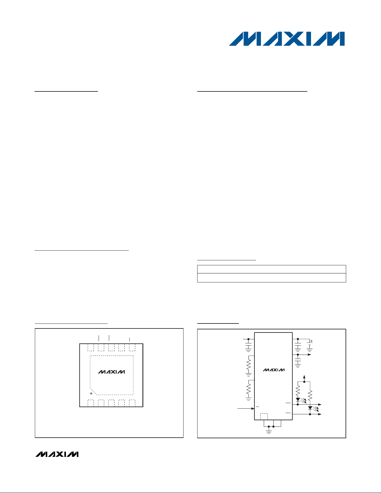
Pin Configuration
PART PIN-PACKAGE TOP MARK
MAX8922LETB+T 10 TDFN-EP* AWN
TOP VIEW
*EP = EXPOSED PAD.
BAT
1019283746
IN
(3mm x 2mm x 0.8mm)
CHG
POKSETI
MAX8922L
GND
TDFN
TEST
LDO
EN/SETMIN
*EP
5
USB/AC ADAPTER
4.45V TO 30V
IN
SETI
R
SETI
MAX8922L
MIN
R
MIN
EN\SET
EP
GND
TEST
BAT
LDO
SYSTEM SUPPLY
CHG
POK
Page 2
MAX8922L
30V Li+ Linear Battery Charger
with GSM Test Mode in 3mm x 2mm TDFN
2 _______________________________________________________________________________________
ABSOLUTE MAXIMUM RATINGS
ELECTRICAL CHARACTERISTICS
(VIN= 5V, V
BAT
= 4V, V
EN/SET
= 0V, TA= -40°C to +85°C, typical values are at TA= +25°C, unless otherwise noted.) (Note 1)
Stresses beyond those listed under “Absolute Maximum Ratings” may cause permanent damage to the device. These are stress ratings only, and functional
operation of the device at these or any other conditions beyond those indicated in the operational sections of the specifications is not implied. Exposure to
absolute maximum rating conditions for extended periods may affect device reliability.
IN to GND ..............................................................-0.3V to +30V
BAT, CHG, EN/SET, POK, SETI,
MIN, LDO, TEST to GND ......................................-0.3V to +6V
Continuous Power Dissipation (T
A
= +70°C)
10-Pin (3mm x 2mm) TDFN
(derate 14.9mW/°C above +70°C)..........................1188.7mW
Operating Temperature Range ...........................-40°C to +85°C
Junction Temperature Range ............................-40°C to +150°C
Storage Temperature Range .............................-65°C to +150°C
Lead Temperature (soldering, 10s) .................................+300°C
IN
Input Voltage Range 028V
Input Voltage Operating Range (Note 2) 4.45 7 V
Input Undervoltage Threshold
(UVLO)
Input Overvoltage Threshold
(OVP)
IN-to-BAT On-Resistance VIN = 4.15V, V
IN-to-BAT Comparator Threshold
BAT
BAT Regulation Voltage I
Battery Removal Detection
Threshold
Charging Current
Soft-Start Time Ramp time to fast-charge current 250 µs
BAT Precharge Threshold V
Precharge Current 80 mA
BAT Leakage Current VIN = 0V, V
PARAMETER CONDITIONS MIN TYP MAX UNITS
rising, 500mV hysteresis (typ) 3.80 3.90 4.00 V
V
IN
rising, 200mV hysteresis (typ) 7.2 7.5 7.8 V
V
IN
I
= 0mA, charge mode 700 1300
BAT
V
= 5V, standby mode 250 440Input Supply Current
EN/SET
= V
V
IN
VIN rising 120 250 500
V
IN
BAT
V
BAT
Hysteresis 0.2
Default fast-charge current, V
EN/SET = one pulse with low > 4ms, R
one-pulse mode, V
EN/SET = two pulses with low > 4ms, V
EN/SET = three pulses with low > 4ms,
V
BAT
BAT
, shutdown mode 200
BAT
= 4V 0.35 Ω
BAT
falling 100
= 100mA
rising 4.67
= 3.5V (Note 3)
rising, 300mV hysteresis (typ) 2.5 V
= 4.2V 1 5 µA
BAT
TA = +25°C 4.179 4.2 4.221
T
= 3.5V
BAT
= -40°C to +85°C 4.158 4.2 4.242
A
= 3.5V 365 400 435
BAT
= 3kΩ,
SETI
= 3.5V 80 90 100
BAT
460 500 540
2350
µA
mV
V
V
mA
Page 3
MAX8922L
30V Li+ Linear Battery Charger
with GSM Test Mode in 3mm x 2mm TDFN
_______________________________________________________________________________________ 3
ELECTRICAL CHARACTERISTICS (continued)
(VIN= 5V, V
BAT
= 4V, V
EN/SET
= 0V, TA= -40°C to +85°C, typical values are at TA= +25°C, unless otherwise noted.) (Note 1)
Note 1: Limits are 100% production tested at T
A
= +25°C. Limits over the operating temperature range are guaranteed by design
and characterization.
Note 2: Guaranteed by undervoltage- and overvoltage-threshold testing. If V
BAT
= 4.2V, VINneeds to be > 4.2V + 250mV (typ) to
start normal operation. After the MAX8922L turns on, it can operate until V
BAT
+ 100mV (typ). For complete charging, the
input voltage must be > 4.45V. See the
Input Sources
section.
Note 3: Used for factory GSM RF calibration. 217Hz, 12.5% current pulse, T
A
= +25°C. Not for continuous charge current.
Note 4: Not tested. Design guidance only.
LDO
Minimum LDO Bypass
Capacitance
LDO Regulated Output Voltage I
LDO Output-Current Limit 100 mA
EN/SET
Logic Input Thresholds
Program Lock Time 4ms
Shutdown Delay VIN = 5V, EN/SET from low to high 4 ms
t
LOW
t
HIGH
Pulldown Resistor 2MΩ
POK, CHG
Logic Output Voltage, Low I
Logic Output Current, High V
CHG
Top-Off Threshold
Detection Delay I
THERMAL LOOP
Thermal-Limit Temperature
Thermal-Limit Gain Reduction of I
PARAMETER CONDITIONS MIN TYP MAX UNITS
= 10mA, VIN = 5V 4.8 4.94 V
LDO
Rising 1.4
Falling 0.4
(Note 4) 100 1400
(Note 4) 100 1400
= I
POK,
POK
I
falling,
BAT
battery is
charged
falls below top-off threshold 2 4 6 ms
BAT
Junction temperature when the charge current is
reduced, T
= 5mA 0.05 0.2 V
CHG
= V
= 5.5V, VIN = 0V
CHG
rising
J
for increase of TJ, default mode -28 mA/°C
BAT
Default top-off threshold, hysteresis
(typ) = 80mA
EN/SET = one pulse, R
1.875kΩ, hysteresis (typ) = 130mA
EN/SET = two pulses, hysteresis
(typ) = 22mA
TA = +25°C 0.001 1
T
= +85°C 0.01
A
60 80 100
=
MIN
60 80 100
50 60 70
+105 °C
1µF
V
µs
µA
mA
Page 4
MAX8922L
30V Li+ Linear Battery Charger
with GSM Test Mode in 3mm x 2mm TDFN
4 _______________________________________________________________________________________
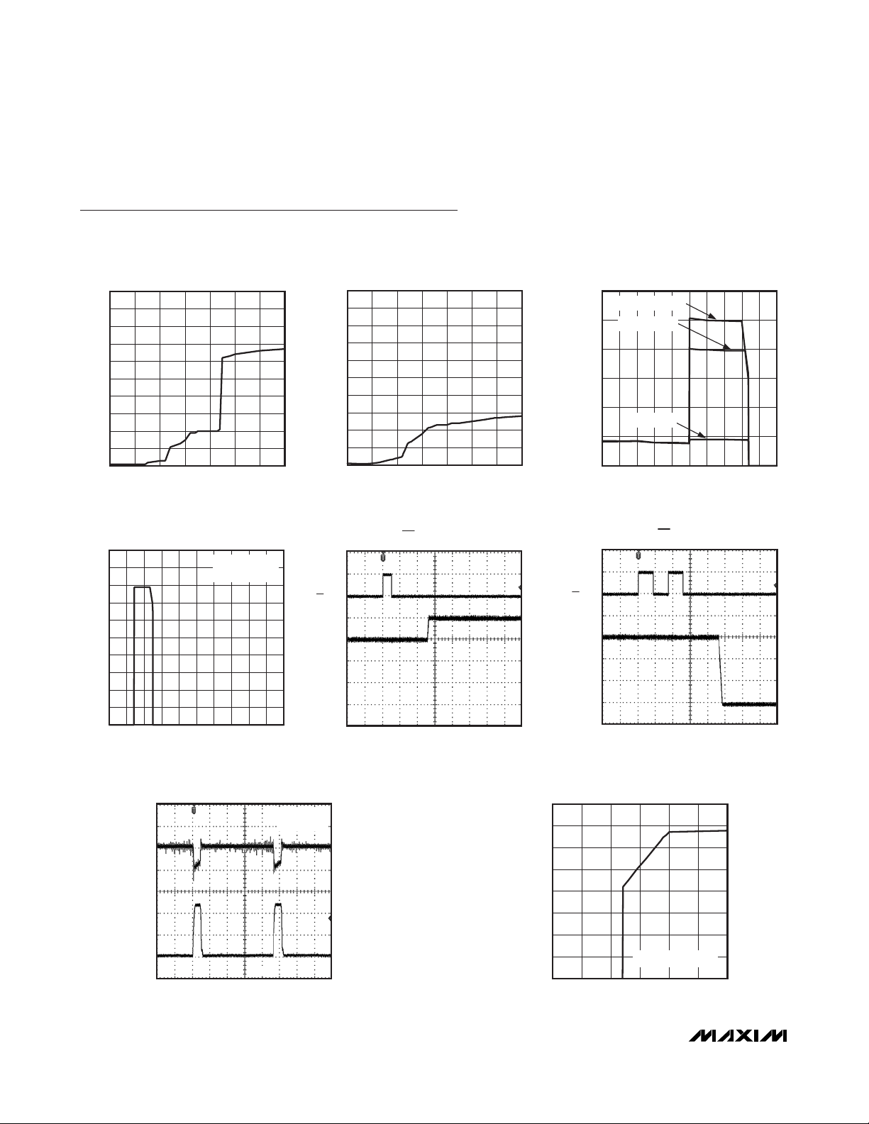
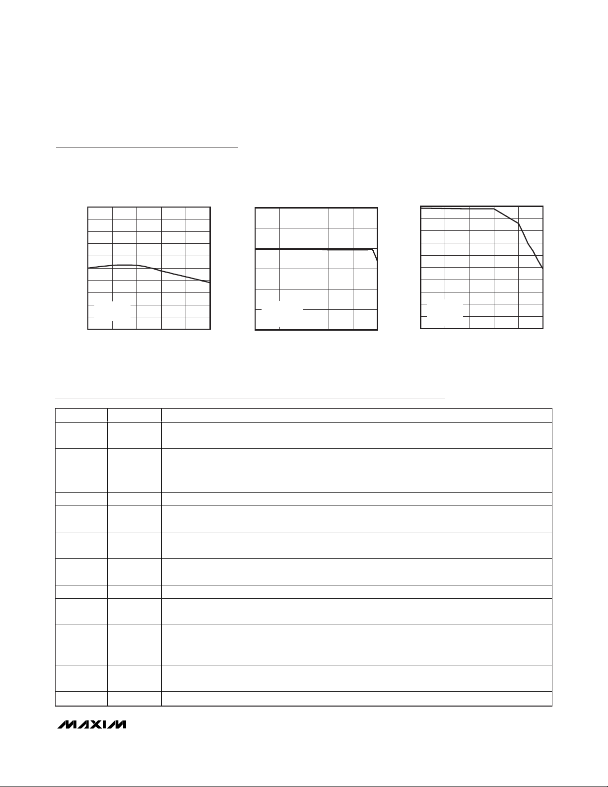
Typical Operating Characteristics
(VIN= 5V, V
EN/SET
= 0V. V
BAT
= 4V, MAX8922L Evaluation Kit. TA= +25°C, unless otherwise noted.)
SUPPLY CURRENT vs.
SUPPLY VOLTAGE
1.0
0.9
0.8
0.7
0.6
0.5
0.4
0.3
SUPPLY CURRENT (mA)
0.2
0.1
0
07
SUPPLY VOLTAGE (V)
CHARGE CURRENT vs.
SUPPLY VOLTAGE
500
450
400
350
300
250
200
150
CHARGE CURRENT (mA)
100
50
0
030
SUPPLY VOLTAGE (V)
653 421
400mA DEFAULT
V
= 4V
BAT
272418 216 9 12 153
DISABLED SUPPLY CURRENT vs.
1.0
0.9
MAX8922 toc01
0.8
0.7
0.6
0.5
0.4
0.3
0.2
STANDBY SUPPLY CURRENT (mA)
0.1
0
07
CHARGE CURRENT WITH ONE
MAX8922 toc04
V
EN/SET
I
BAT
SUPPLY VOLTAGE
SUPPLY VOLTAGE (V)
EN/SET PULSE
1ms/div
653 421
MAX8922 toc05
MAX8922 toc02
5V/div
0
500mA
400mA
100mA/div
0
CHARGE CURRENT vs.
BATTERY VOLTAGE
600
500mA SETI MODE
500
400mA PRESET
400
300
200
CHARGE CURRENT (mA)
100
90mA PRESET
0
05
BATTERY VOLTAGE (V)
4321
MAX8922 toc03
CHARGE CURRENT WITH TWO
V
EN/SET
EN/SET PULSES
I
BAT
1ms/div
MAX8922 toc06
5V/div
0
400mA
100mA/div
0
GSM TRANSIENT RESPONSE
V
BAT
I
BAT
1ms/div
MAX8922 toc07
NO BATTERY
C
= 68µF
BAT
200mv/div
AC-COUPLED
1A/div
0A
800
700
600
500
400
300
CHARGE CURRENT (mA)
200
100
INPUT VOLTAGE HEADROOM
I
FAST-CHARGE
0
0 300
VIN - V
(mV)
BAT
CHARGE CURRENT vs.
MAX8922 toc08
= 677mA
25020050 100 150
Page 5
MAX8922L
30V Li+ Linear Battery Charger
with GSM Test Mode in 3mm x 2mm TDFN
_______________________________________________________________________________________ 5
Typical Operating Characteristics (continued)
(VIN= 5V, V
EN/SET
= 0V. V
BAT
= 4V, MAX8922L Evaluation Kit. TA= +25°C, unless otherwise noted.)
Pin Description
BAT REGULATION VOLTAGE ACCURACY
1.0
0.8
0.6
0.4
0.2
0
-0.2
-0.4
REGULATION ACCURACY (%)
BAT
-0.6
V
-0.8
-1.0
-40 85
PIN NAME FUNCTION
1IN
2 SETI
3 GND Ground
4LDO
5MIN
6 EN/SET
7 TEST Factory Test Input. Connect to GND.
8 CHG
9 POK
10 BAT
— EP Exposed Pad. Connect to the GND plane for increased thermal dissipation.
vs. AMBIENT TEMPERATURE
VIN = 5V
NO BATTERY
AMBIENT TEMPERATURE (°C)
DC Input Supply. Connect IN to V
Bypass IN to GND with a 1µF or larger ceramic capacitor.
Charge-Current Program and Fast-Charge Current Monitor. Output current from SETI is 1000µA per
ampere of battery-charging current. Set the charging current by connecting a resistor (R
1) from SETI to GND. I
is not used.
4.94V Regulated LDO Output with Input Overvoltage Protection. Bypass LDO to GND with a 1µF or
larger ceramic capacitor. LDO can be used to supply low-voltage-rated USB systems.
Top-Off Current Threshold Programmable Input. I
(external SETI) is not used.
Active-Low Enable Input. EN/SET is used for programming fast-charge current and GSM test mode. For
detailed descriptions, see the Charger-Enable and Program Input (
Charging-Status Output. CHG is internally pulled low when the charger is in prequalification or fast-
charge mode. CHG is high impedance when the charger is in top-off or disabled.
Input Power-OK Monitor. POK is an open-drain output that is internally pulled low when V
than V
than V
Battery Connection. The IC delivers charging current and monitors battery voltage using BAT. Bypass
BAT to GND with a 2.2µF or larger ceramic capacitor. BAT is high impedance when the IC is disabled.
603510-15
and lower than V
UVLO
or greater than V
UVLO
600
MAX8922 toc09
500
400
300
200
CHARGE CURRENT (mA)
100
0
FAST-CHARGE
CHARGE CURRENT vs.
AMBIENT TEMPERATURE
400mA PRESET
VIN = 5V
V
= 4V
BATT
AMBIENT TEMPERATURE (°C)
> 4V and (VIN - V
IN
= 1500V/R
and VIN > V
OVP
or VIN < V
OVP
MAX8922 toc10
60
3510-15-40 85
) ≥ 250mV up to a 7V charging source.
BAT
. Connect to GND if pulse 1 mode (external SETI)
SETI
= 150V/R
MIN
+ 250mV. POK is high impedance when V
BAT
+ 100mV.
BAT
CHARGE CURRENT vs.
AMBIENT TEMPERATURE (1A CHARGE)
1000
900
800
700
600
500
400
300
CHARGE CURRENT (mA)
I
R
200
100
= 1.5k
SETI
V
= 5V
IN
V
= 4V
BATT
0
-40 85
AMBIENT TEMPERATURE (°C)
3510-15
SETI
Connect to GND if pulse 1 mode
MIN.
EN
/SET) section.
is greater
IN
60
in Figure
is less
IN
MAX8922 toc11
Page 6
MAX8922L
30V Li+ Linear Battery Charger
with GSM Test Mode in 3mm x 2mm TDFN
6 _______________________________________________________________________________________
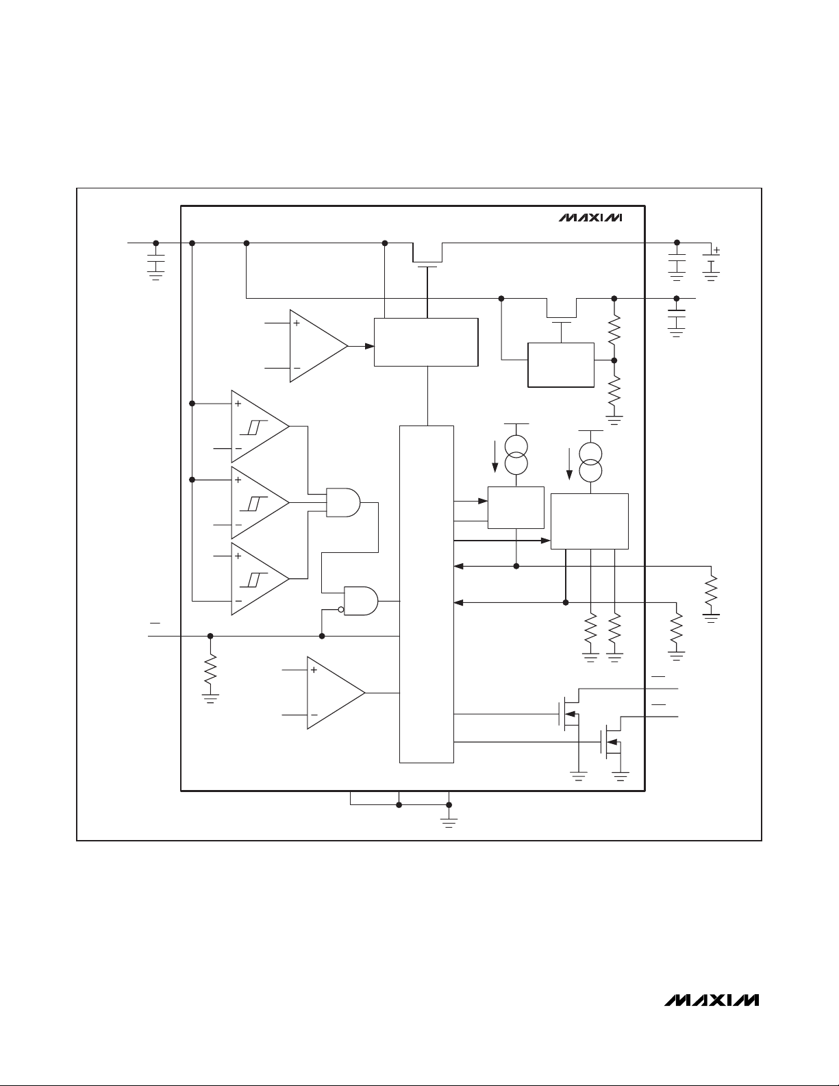
Figure 1. MAX8922L Functional Diagram
4.45V TO 30V
IN
7.5V
EN/SET
3.9V
BAT
Tj(DIE)
+105°C
CC/CV
REGULATOR
CHARGE
AND
LOGIC
CONTROL
TOP-OFF
SWITCH
LDO
CONTROL
FAST-CHARGE
MAX8922
SWITCH
BAT
LDO
MIN
SETI
Li+
R
MIN
R
SETI
BAT
2.5V
PRECHARGE
EP
GND
TEST
POK
CHG
Page 7

Detailed Description
The MAX8922L is designed to charge a single-cell Li+
battery from a DC source voltage between 4.45V and
7V, while VINcan withstand up to 30V. The fast-charge
current and top-off current thresholds are programmable with EN/SET, SETI, and MIN.
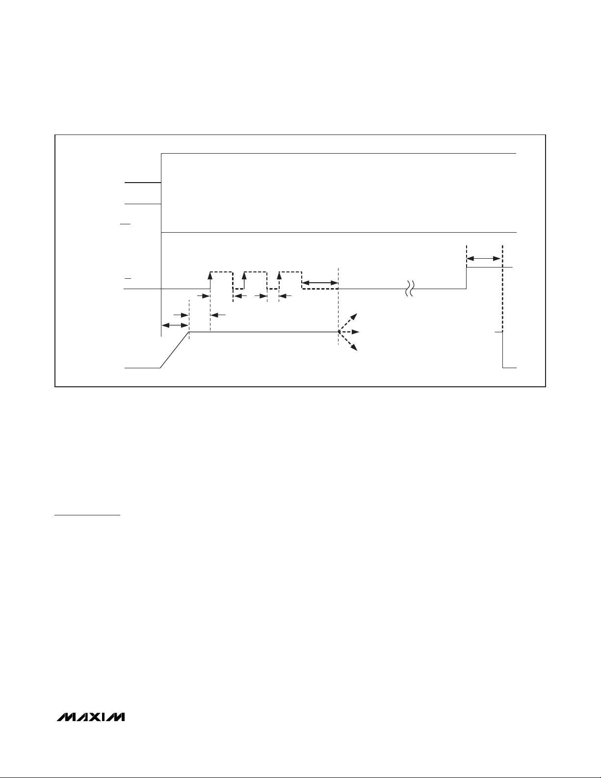
Charger-Enable and Program Input
(
EN
/SET)
EN/SET is an active-low logic input that enables the
charger. Drive EN/SET high longer than 4ms to disable
the charger-control circuitry. If EN/SET is left unconnected, an internal 2MΩ pulldown resistor enables
400mA fast-charge current by default. The pulse programming scheme shown in Table 1 and Figure 3 is
used to program the charge current and GSM test
mode. There are four different fast-charge current
states. Default fast-charge current state is 400mA
mode. More than three pulses are interpreted to 90mA
mode. After programming is locked, the MAX8922L
ignores pulses until the IC is disabled/enabled or input
power is cycled. Each fast-charge state is locked after
a 4ms logic-low is asserted on EN/SET, followed by
programming pulses. However, during default mode, if
EN/SET does not receive any pulses, the charger stays
in default mode unlocked indefinitely.
Debounce Timer
To prevent the MAX8922L from charging the battery
momentarily upon IN power-up with EN/SET held low, a
2ms (typ) debounce timer delays the charging loop
upon power-up. If EN/SET is logic-low or unconnected
(pulled down by an internal pulldown resistor) during IN
power-up, the charger starts charging the battery 2ms
after V
UVLO
< VIN< V
OVP
and V
BAT
+ 250mV < VIN. If
EN/SET is logic-high during IN power-up, the charger
does not charge the battery.
Soft-Start
To prevent input transients, the rate of change of the
charge current is limited when the charger is turned on
or changes its current compliance. It takes approximately 250µs (typ) (t
SOFTSTART
) for the charger to go
from 0mA to the maximum fast-charge current.
Thermal-Limit Control
The MAX8922L features a thermal limit that reduces the
charge current when the die temperature exceeds
+105°C. As the temperature increases above +105°C,
the IC decreases the charge current by 28mA/°C.
Charge-Indicator Output (
CHG
)
CHG is an open-drain output that indicates charger status. CHG goes low during charging in prequalification
or fast-charge mode. The CHG internal open-drain
MOSFET turns off when the charge current reaches the
top-off threshold. The CHG status is latched after the
top-off threshold is reached. The latch can be reset as
follows:
• Disable and re-enable the MAX8922L.
• Input power is cycled.
• Battery-charge current increases greater than the
top-off threshold + hysteresis.
When the MAX8922L is used in conjunction with a
microprocessor, connect a pullup resistor between
CHG and the logic I/O voltage to indicate charge status
to the µP. Alternatively, CHG can sink 5mA or more for
an LED charge indicator.
MAX8922L
30V Li+ Linear Battery Charger
with GSM Test Mode in 3mm x 2mm TDFN
_______________________________________________________________________________________ 7
Table 1. Charge-Current Pulse Settings
CHARGE CURRENT DEFAULT
I
(mA) 400mA
BAT
NUMBER OF PULSES + > 4ms
LOGIG-LOW
One SETI, resistor programmable
Two 90mA
Three 2.3A (GSM test)
Four and more 90mA
FAST-CHARGE CURRENT SETTING
Page 8

MAX8922L
Power-OK Indicator (
POK
)
The MAX8922L contains an open-drain POK output that
goes low when VINis greater than V
UVLO
and lower than
V
OVP
and VINexceeds the battery voltage by 250mV.
Once charging has started, charging is sustained with
inputs as low as 3.5V, as long as the input voltage
remains above the battery voltage by at least 100mV.
POK status should be maintained even though the
charger is disabled by EN/SET. When V
IN
> V
OVP
, POK
is high impedance.
30V Li+ Linear Battery Charger
with GSM Test Mode in 3mm x 2mm TDFN
8 _______________________________________________________________________________________
Figure 2. Charger State Diagram
CHARGER LOOP DEFAULT IS OFF;
IF EN/SET = LOW UPON POK.
CHARGER LOOP
ACTIVATES AFTER 4ms
POR DEBOUNCE
ASYNCHRONOUS
FROM ANYWHERE
= HIGH > 4ms
t
EN/SET
STANDBY MODE
CHARGER = OFF
POK = LOW
CHG = HIGH IMPEDANCE
V
UVLO
V
< VIN < V
> V
IN
BAT
OVP
+ 250mV
AND
SHUTDOWN
CHARGER = OFF
POK = HIGH IMPEDANCE
CHG = HIGH IMPEDANCE
V
< V
EN/SET = LOW
OR V
OR V
BAT
IN
UVLO
> V
IN
OVP
+ 100mV > VIN
ASYNCHRONOUS
FROM ANYWHERE
V
< V
IN
UVLO
> V
OR V
IN
OR V
+ 100mV > VIN
BAT
OVP
PREQUALIFICATION
PRECHARGE CURRENT
V
< 2.5V
BAT
V
> I
TOP-OFF
+ HYSTERESIS
I
CHG
POK = LOW
CHG = LOW
< 2.2V V
BAT
FAST CHARGE
(PULSE PROGRAMMABLE)
100% CHARGER CURRENT
POK = LOW
CHG = LOW
FULL BATTERY
= 4.2V
V
BAT
POK = LOW
CHG = HIGH IMPEDANCE
> 2.5V
BAT
< I
I
CHG
TOP-OFF
PULSE 3
MODE DOES NOT HAVE
PRECHARGE STATE
FULL BATTERY CONTINUES
TO REGULATE V
BAT
TO 4.2V
POK = (V
AND (V
OVP
IN
> VIN > V
- V
BAT
UVLO
) > 250mV
)
Page 9
LDO Output
The LDO is preset to an output voltage of 4.94V and a
100mA current limit (typ). The LDO is powered from IN
and has input overvoltage protection. The LDO is on if a
valid input is present (V
UVLO
< VIN< V
OVP
).
Bypass LDO to GND with a 1µF or larger ceramic
capacitor. The LDO can be used to supply low-voltagerated USB systems.
Applications Information
Fast-Charge Current Settings
In pulse 1 mode, the maximum charging current is programmed by an external resistor connected from SETI
to GND (R
SETI
). Calculate R
SETI
as follows:
R
SETI
= 1500V/I
FAST-CHARGE
where I
FAST-CHARGE
is in amperes and R
SETI
is in
ohms. SETI can be used to monitor the fast-charge current level in the one-pulse mode (R
SETI
mode). The output current from SETI is 1000µA per ampere of
charging current.
The output voltage at SETI is proportional to the charging current (I
CHARGE
) when SETI mode is used for the
fast-charge current:
V
SETI
= I
CHARGE
x R
SETI
/1000
The voltage at ISET is nominally 1.5V at the selected
fast-charge current and decreases with charging current as the cell becomes fully charged or as the thermal-regulation circuitry activates.
Top-Off Current Settings
The top-off charging current is programmed by an
external resistor connected from MIN to GND (R
MIN
) in
the one-pulse mode (R
SETI
mode). Calculate R
MIN
as
follows:
R
MIN
= 150V/I
MIN
where I
MIN
is in amperes and R
MIN
is in ohms.
Capacitor Selection
Connect a 2.2µF ceramic capacitor from BAT to GND
for proper stability. Connect a 1µF ceramic capacitor
from IN to GND. Use a larger input bypass capacitor for
high charging currents to reduce supply noise. All
capacitors should be X5R dielectric or better. Be aware
that some capacitors have large-voltage coefficients,
and should be avoided.
MAX8922L
30V Li+ Linear Battery Charger
with GSM Test Mode in 3mm x 2mm TDFN
_______________________________________________________________________________________ 9
Figure 3. Charge-Current Programming
DC
HIGH IMPEDANCE
POK
123
EN
t
SOFTSTART
I
FAST
t
HIGH
NO TIME LIMIT
400mA SETTING (DEFAULT)
t
LOW
PULL LOW
> 4ms
> 4ms
SETI MODE (1 PULSE + > 4ms LOW)
90mA MODE (2 PULSES + > 4ms LOW)
GSM TEST MODE
(3 PULSES + > 4ms LOW)
OFF
Page 10

MAX8922L
Thermal Considerations
The MAX8922L is in a thermally enhanced TDFN package with an exposed pad. Connect the exposed pad of
the package to a large copper ground plane to provide a
thermal contact between the device and the circuit board.
The exposed pad transfers heat away from the device,
allowing the IC to charge the battery with maximum current, while minimizing the increase in die temperature.
Input Sources
The MAX8922L operates from well-regulated DC
sources. The charger input voltage range is 4.45V to
7V. The device survives input voltages up to 30V without damage to the IC. If the input voltage is greater
than 7.5V (typ), the IC stops charging. An appropriate
power supply must provide at least 4.2V plus the voltage drop across the internal-pass transistor when
sourcing the desired peak charging current.
V
IN(MIN)
> 4.2V + I
FAST-CHARGE(MAX)
x R
ON
where RONis the input-to-BAT resistance. Failure to
meet this requirement results in an incomplete charge
or increased charge time.
Recommended PCB Layout and Routing
Place all bypass capacitors for IN and BAT as close as
possible to the IC. Connect the battery to BAT as close
as possible to the IC to provide accurate battery voltage sensing. Provide a large copper ground plane to
allow the exposed pad to sink heat away from the
device. Make all high-current traces short and wide to
minimize voltage drops. A sample layout is available in
the MAX8922L Evaluation Kit to speed designs.
Typical Application Circuits
AC Adapter Charge
Figure 4 shows the MAX8922L as a Li+ battery charger
with an AC adapter. The MAX8922L detects the presence of an input supply resulting in POK pulled low.
Once POK is pulled low, the MAX8922L begins charging the battery when EN/SET is low or unconnected.
The system can program the charge current by EN/SET
pulses. By monitoring CHG, the system can detect the
top-off threshold and terminate the charge through
EN/SET. The MAX8922L also provides an overvoltageprotected 4.94V LDO output to a low-voltage-rated USB
system input.
30V Li+ Linear Battery Charger
with GSM Test Mode in 3mm x 2mm TDFN
10 ______________________________________________________________________________________
Figure 4. AC Adapter Charger Application
AC
ADAPTER
C1
1µF
R1
1.87kΩ
IN
MIN
SETI
R2
3kΩ
EP
MAX8922L
TEST
GND
BAT
LDO
POK
CHG
EN/SET
C2
2.2µF
C3
1µF
VI/O
4.2V
Li+
SYSTEM
VBUS
GPIO
GPIO
GPIO
Page 11

USB Charge
The universal serial bus (USB) provides a high-speed
serial communications port as well as power for the
remote device. The MAX8922L can be configured to
charge a single Li+ battery at the highest current possible from the host port. Figure 5 shows the MAX8922L as
a USB battery charger. The microprocessor enumerates
the host to determine its current capability. The system
can program the charge current to 90mA, I
SETI
, or
400mA by EN/SET pulses if the host port is capable. The
MAX8922L also provides an overvoltage-protected 4.94V
LDO output to a low-voltage-rated USB system input.
GSM Test Mode
Figure 6 shows the MAX8922L in a GSM test mode. By
sending three pulses to EN/SET, the MAX8922L goes
into GSM test mode. GSM PA can pull up to 2.3A for
576µs once every 217Hz from the MAX8922L’s output.
The configuration in Figure 6 is used for system development, testing, and calibrations in the production or
design stage.
MAX8922L
30V Li+ Linear Battery Charger
with GSM Test Mode in 3mm x 2mm TDFN
______________________________________________________________________________________ 11
Figure 5. USB-Powered Li+ Battery-Charger Application
USB
CABLE
1µF
C1
IN
BAT
C2
2.2µF
4.2V
Li+
SYSTEM
MIN
R1
1.87kΩ
MAX8922L
SETI
R2
3kΩ
TEST
GND
EP
LDO
POK
CHG
EN/SET
C3
1µF
VI/O
VBUS
GPIO
GPIO
GPIO
Page 12

MAX8922L
30V Li+ Linear Battery Charger
with GSM Test Mode in 3mm x 2mm TDFN
12 ______________________________________________________________________________________
Figure 6. GSM Test Mode
Chip Information
PROCESS: BiCMOS
GSM PA
USB
CABLE
C1
1µF
1.87kΩ
3kΩ
IN
MIN
R1
MAX8922L
SETI
R2
GND
EP
TEST
BAT
LDO
POK
CHG
EN/SET
C2
68µF
C3
1µF
SYSTEM
VBUS
VI/O
GPIO
GPIO
GPIO
Page 13

MAX8922L
PACKAGE TYPE PACKAGE CODE DOCUMENT NO.
10 TDFN-EP T1032N-1
21-0429
Package Information
For the latest package outline information and land patterns, go to www.maxim-ic.com/packages. Note that a "+", "#", or "-" in the
package code indicates RoHS status only. Package drawings may show a different suffix character, but the drawing pertains to the
package regardless of RoHS status.
30V Li+ Linear Battery Charger
with GSM Test Mode in 3mm x 2mm TDFN
______________________________________________________________________________________ 13
TDFN.EPS
Page 14

MAX8922L
30V Li+ Linear Battery Charger
with GSM Test Mode in 3mm x 2mm TDFN
Maxim cannot assume responsibility for use of any circuitry other than circuitry entirely embodied in a Maxim product. No circuit patent licenses are
implied. Maxim reserves the right to change the circuitry and specifications without notice at any time.
14
____________________Maxim Integrated Products, 120 San Gabriel Drive, Sunnyvale, CA 94086 408-737-7600
© 2009 Maxim Integrated Products Maxim is a registered trademark of Maxim Integrated Products, Inc.
Package Information (continued)
For the latest package outline information and land patterns, go to www.maxim-ic.com/packages. Note that a "+", "#", or "-" in the
package code indicates RoHS status only. Package drawings may show a different suffix character, but the drawing pertains to the
package regardless of RoHS status.
 Loading...