

Page 1
General Description
The MAX8903A is an integrated 1-cell Li+ charger and
Smart Power Selector™ with dual (AC adapter and
USB) power inputs. The switch mode charger uses a
high switching frequency to eliminate heat and allow
tiny external components. It can operate with either
separate inputs for USB and AC adapter power, or from
a single input that accepts both. All power switches for
charging and switching the load between battery and
external power are included on-chip. No external
MOSFETs, blocking diodes, or current-sense resistors
are required.
The MAX8903A features optimized smart power control
to make the best use of limited USB or adapter power.
Battery charge current and SYS output current limit are
independently set. Power not used by the system
charges the battery. Charge current and SYS output
current limit can be set up to 2A while USB input current can be set to 100mA or 500mA. Automatic input
selection switches the system from battery to external
power. The DC input operates from 4.15V to 16V with
up to 20V protection, while the USB input has a range
of 4.1V to 6.3V with up to 8V protection.
The MAX8903A internally blocks current from the battery and system back to the DC and USB inputs when
no input supply is present. Other features include prequal charging and timer, fast charge timer, overvoltage
protection, charge status and fault outputs, power-OK
monitors, and a battery thermistor monitor. In addition,
on-chip thermal limiting reduces battery charge rate
and AC adapter current to prevent charger overheating. The MAX8903A is available in a 4mm x 4mm, 28-pin
thin QFN package.
Applications
PDAs, Palmtops, and Wireless Handhelds
Personal Navigation Devices
Smart Cell Phones
Portable Multimedia Players
Mobile Internet Devices
Ultra Mobile PCs
Features
♦ Efficient DC-DC Converter Eliminates Heat
♦ 4MHz Switching for Tiny External Components
♦ Instant On—Works with No Battery or Low
Battery
♦ Dual Current-Limiting Input Circuits—AC Adapter
or USB
Automatic Adapter/USB/Battery Switchover to
Support Load Transients
50mΩ System-to-Battery Switch
Supports USB Spec
♦ Thermistor Monitor
♦ Integrated Current-Sense Resistor
♦ No External MOSFETS or Diodes
♦ 4.1V to 16V Input Operating Voltage Range
MAX8903A
2A 1-Cell Li+ DC-DC Charger for USB*
and Adapter Power
________________________________________________________________
Maxim Integrated Products
1
19-4410; Rev 0; 12/08
For pricing, delivery, and ordering information, please contact Maxim Direct at 1-888-629-4642,
or visit Maxim’s website at www.maxim-ic.com.
EVALUATION KIT
AVAILABLE
Pin Configuration appears at end of data sheet.
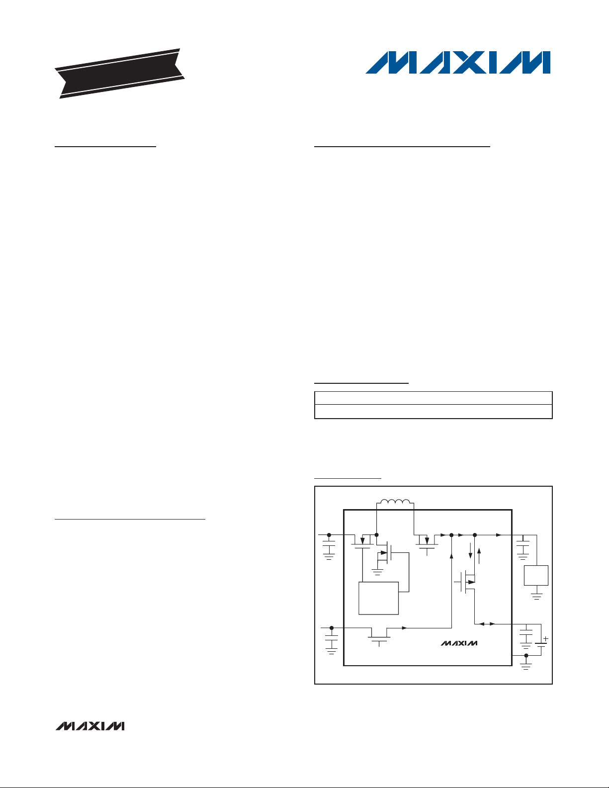
Typical Operating Circuit
*Protected by US Patent #6,507,172.
Smart Power Selector is a trademark of Maxim Integrated
Products, Inc.
Ordering Information
+
Denotes a lead(Pb)-free/RoHS-compliant package.
**
EP = Exposed pad.
PART TEMP RANGE PIN-PACKAGE
MAX8903AETI+ -40°C to +85°C
28 Thin QFN-EP**
AC
ADAPTER
OR USB
USB
DC
USB
LX
PWM
STEP-DOWN
CS
SYS
LOAD
CHARGE
CURRENT
CURRENT
CHARGE AND
SYS LOAD
SWITCH
BAT
SYSTEM
LOAD
BATTERY
MAX8903A
GND
Page 2
MAX8903A
2A 1-Cell Li+ DC-DC Charger for USB*
and Adapter Power
2 _______________________________________________________________________________________
ELECTRICAL CHARACTERISTICS
(VDC= V
USB
= 5V, V
BAT
= 4V, circuit of Figure 2, TA= -40°C to +85°C, unless otherwise noted. Typical values are at TA= +25°C.)
(Note 1)
Stresses beyond those listed under “Absolute Maximum Ratings” may cause permanent damage to the device. These are stress ratings only, and functional
operation of the device at these or any other conditions beyond those indicated in the operational sections of the specifications is not implied. Exposure to
absolute maximum rating conditions for extended periods may affect device reliability.
ABSOLUTE MAXIMUM RATINGS
DC, LX, DCM to GND .............................................-0.3V to +20V
DC to SYS .................................................................-6V to +20V
BST to GND ...........................................................-0.3V to +26V
BST TO LX ................................................................-0.3V to +6V
USB to GND .............................................................-0.3V to +9V
USB to SYS..................................................................-6V to +9V
VL to GND ................................................................-0.3V to +6V
THM, IDC, ISET, CT to GND .........................-0.3V to (VL + 0.3V)
DOK, FLT, CEN, UOK, CHG, USUS,
BAT, SYS, IUSB, CS to GND ................................-0.3V to +6V
SYS to BAT ...............................................................-0.3V to +6V
PG, EP (exposed pad) to GND .............................-0.3V to +0.3V
DC Continuous Current (total in two pins)......................2.4A
RMS
USB Continuous Current.......................................................1.6A
LX Continuous Current (total in two pins).......................2.4A
RMS
CS Continuous Current (total in two pins) ......................2.4A
RMS
SYS Continuous Current (total in two pins) .......................3A
RMS
BAT Continuous Current (total in two pins) .......................3A
RMS
Continuous Power Dissipation (TA= +70°C)
28-Pin Thin QFN-EP
Multilayer (derate 28.6mW/°C above +70°C) ..........2286mW
28-Pin Thin QFN-EP
Single-Layer (derate 20.8mW/°C above +70°C)...1666.7mW
Operating Temperature Range ...........................-40°C to +85°C
Junction Temperature Range ............................-40°C to +150°C
Storage Temperature Range .............................-65°C to +150°C
Lead Temperature (soldering, 10s) .................................+300°C
DC INPUT
DC Operating Range 4.15 16 V
DC Undervoltage Threshold
DC Overvoltage Threshold
DC Supply Current
DC High-Side Resistance 0.15 Ω
DC Low-Side Resistance 0.15 Ω
DC-to-BAT Dropout Resistance 0.31 Ω
DC-to-BAT Dropout Voltage
Switching Frequency
DC Step-Down Output CurrentLimit Step Range
DC Step-Down Output Current
Limit
DC Soft-Start Time
PARAMETER CONDITIONS MIN TYP MAX UNITS
When V
rising, 500mV typical hysteresis
When V
hysteresis
Charger enabled, no switching, V
Charger enabled, f = 3MHz, VDC = 5V 15
C har g er enab l ed , V
C har g er enab l ed , V
V
DCM
When SYS regulation and charging stops, V
200mV hysteresis
VDC = 8V, V
V
DC
V
DC
No valid USB input 1 ms
Valid USB input before soft-start 20 µs
goes low, V
DOK
goes high, VDC rising, 500mV typical
DOK
= 0V, V
USUS
= 4V 4
BAT
= 5V, V
= 6V, V
= 3V 3
BAT
= 4V
SYS
DC
= 0V , 100m A U S B m od e ( N ote 2) 1 2
C E N
= 5V , 100m A U S B m od e ( N ote 2) 1 2
C E N
= 5V 0.10 0.25
No valid USB input 3.9 4.0 4.1
Valid USB input 4.0 4.3 4.4
16.5 17 17.5 V
= 5V 2.3 4
SYS
falling,
DC
R
= 3kΩ 1900 2000 2100
IDC
R
= 6kΩ 950 1000 1050
IDC
= 12kΩ 450 500 550
R
IDC
01530mV
0.5 2 A
V
mA
MHz
mA
Page 3
MAX8903A
2A 1-Cell Li+ DC-DC Charger for USB*
and Adapter Power
_______________________________________________________________________________________ 3
ELECTRICAL CHARACTERISTICS (continued)
(VDC= V
USB
= 5V, V
BAT
= 4V, circuit of Figure 2, TA= -40°C to +85°C, unless otherwise noted. Typical values are at TA= +25°C.)
(Note 1)
DC Output Current
500mA USB Mode
(Note 3)
DC Output Current
100mA USB Mode
(Note 2)
SYS to DC Reverse Current
Blocking
USB INPUT
USB Operating Range 4.1 6.3 V
USB Standoff Voltage 8V
USB Undervoltage Threshold When V
USB Overvoltage Threshold When V
USB Current Limit
Minimum USB to BAT Headroom 0 15 30 mV
USB to SYS Dropout Resistance 0.2 0.35 Ω
USB Soft-Start Time
SYS OUTPUT
Minimum SYS Regulation Voltage I
Regulation Voltage I
Load Regulation I
CS to SYS Resistance VDC = 6V, V
SYS to CS Leakage V
BAT to SYS Resistance VDC = V
BAT to SYS Reverse Regulation
Voltage
SYS Undervoltage Threshold SYS falling, 200mV hysteresis (Note 4) 1.8 1.9 2.0 V
BATTERY CHARGER
BAT Regulation Voltage I
Charger Restart Threshold Change in V
BAT Prequal Threshold V
Prequal Charge Current Percentage of fast-charge current set at ISET 10 %
PARAMETER CONDITIONS MIN TYP MAX UNITS
V
= 0V, V
DCM
V
= 0V, V
DCM
V
= 5.5V, VDC = 0V 0.01 µA
SYS
UOK
UOK
V
= 0V (100mA setting) 90 95 100
IUSB
V
= 5V (500mA setting) 450 475 500
IUSB
I
= I
SYS
BAT
I
= I
SYS
BAT
= 5V (USB suspend mode) 0.115 0.25
V
USUS
V
rising 1 ms
USB
falling below DC UVLO to initiate USB soft-start 20 µs
V
DC
= 1A, V
SYS
= 0A 4.3 4.4 4.5 V
SYS
= 0 to 2A 40 mV/A
SYS
= 5.5V, VDC = VCS = 0V 0.01 µA
SYS
USB
V
= 5V, VDC = 0V, V
USB
= 0mA
BAT
rising, 180mV hysteresis 2.9 3 3.1 V
BAT
= 5V 450 475 500 mA
IUSB
= 0V 90 95 100 mA
IUSB
goes low, V
goes high, V
= 0mA, V
= 0mA, V
< V
BAT
SYS_MIN
= 5V, V
DCM
= 0V, V
BAT
rising, 500mV hysteresis 3.95 4.0 4.05 V
USB
rising, 500mV hysteresis 6.8 6.9 7.0 V
USB
= 0V 1.3 3
CEN
= 5V 0.8 2USB Supply Current
CEN
3.0 V
= 4V, ICS = 1A 0.07 Ω
SYS
= 4.2V, I
IUSB
= 1A 0.05 0.1 Ω
SYS
= 0V, I
= 200mA 50 75 100 mV
SYS
TA = +25°C 4.179 4.2 4.221
= -40°C to +85°C 4.158 4.2 4.242
T
A
from DONE to fast-charge -150 -100 -60 mV
BAT
mA
mA
V
Page 4
MAX8903A
2A 1-Cell Li+ DC-DC Charger for USB*
and Adapter Power
4 _______________________________________________________________________________________
ELECTRICAL CHARACTERISTICS (continued)
(VDC= V
USB
= 5V, V
BAT
= 4V, circuit of Figure 2, TA= -40°C to +85°C, unless otherwise noted. Typical values are at TA= +25°C.)
(Note 1)
DONE Threshold Percentage of fast-charge, I
R
ISET
ISET Output Voltage 1.5 V
ISET Current Monitor Gain 1.25 mA/A
BAT Leakage Current
Charger Soft-Start Time 1.0 ms
Charger Thermal Limit
Temperature
Charger Thermal Limit Gain Charge current = 0 at + 120°C 5 %/°C
CHARGER TIMER
Prequalification Time CCT = 0.15µF 33 min
Fast-Charge Time CCT = 0.15µF 660 min
Timer Accuracy -15 +15 %
Timer Extend Current Threshold
Timer Suspend Current Threshold
Charge Done Delay Time
THERMISTOR MONITOR
THM Threshold, Hot When charging is suspended, 1% hysteresis
THM Threshold, Cold When charging is suspended, 1% hysteresis
THM Threshold, Disabled THM function is disabled below this voltage
THM Input Leakage
THERMAL SHUTDOWN, VL, AND LOGIC I/O: CHG, FLT, DOK, UOK, DCM, CEN, USUS, IUSB
Logic-Input Thresholds
(DCM, CEN, USUS, IUSB)
Logic-Input Leakage Current
(DCM, CEN, USUS, IUSB)
PARAMETER CONDITIONS MIN TYP MAX UNITS
Resistor Range 0.6 2.4 kΩ
R
= 600Ω 1800 2000 2200
ISET
R
= 1.2kΩ 900 1000 1100Fast-Charge Current
ISET
= 2.4kΩ 450 500 550
R
ISET
decreasing 10 %
BAT
No DC or USB input 0.05 4
With valid input power, V
Percentage of fast-charge current below which the timer
clock operates at half-speed
Percentage of fast-charge current below which timer
clock pauses
From done threshold detection until charger turns off and
CHG goes high
THM = GND or VL; TA = +25°C -0.1 +0.001 +0.2
THM = GND or VL; T
High level 1.3
Low level 0.4
Hysteresis 50 mV
= 0 to 5.5V
V
INPUT
= 5V 1 6
CEN
40 50 60 %
16 20 24 %
0.27 x
V
0.73 x
V
0.0254
x V
= +85°C 0.01
A
TA = +25°C 0.001 1
T
= +85°C 0.01
A
0.28 x
VL
0.74 x
VL
0.03 x
VL
100 °C
15 s
0.29 x
V
V
V
VL
VL
VL
V
0.75 x
V
0.036 x
V
VL
VL
VL
mA
µA
V
V
V
µA
V
µA
Page 5
MAX8903A
2A 1-Cell Li+ DC-DC Charger for USB*
and Adapter Power
_______________________________________________________________________________________ 5
ELECTRICAL CHARACTERISTICS (continued)
(VDC= V
USB
= 5V, V
BAT
= 4V, circuit of Figure 2, TA= -40°C to +85°C, unless otherwise noted. Typical values are at TA= +25°C.)
(Note 1)
Note 1: Limits are 100% production tested at T
A
= +25°C. Limits over the operating temperature range are guaranteed by design.
Note 2: For the 100mA USB mode using the DC input, the step-down regulator is turned off and a low-dropout linear regulator is
connected from DC to SYS.
Note 3: For the 500mA USB mode, the actual current drawn from USB is less than the output current due to the input/output current
ratio of the DC-DC converter.
Note 4: For short-circuit protection, SYS sources 25mA below V
SYS
= 400mV, and 50mA for V
SYS
between 400mV and 2V.
Typical Operating Characteristics
(TA = +25°C, unless otherwise noted.)
Logic Output Voltage, Low
(CHG, FLT, DOK, UOK)
Open-Drain Output Leakage
C ur rent, Hi g h (CHG , FLT, DOK, UOK)
VL Output Voltage VDC = V
VL UVLO Threshold VVL falling; 200mV hysteresis 3.2 V
Thermal Shutdown Temperature 160 °C
Thermal Shutdown Hysteresis 15 °C
PARAMETER CONDITIONS MIN TYP MAX UNITS
Sinking 1mA 8 50
Sinking 10mA 80
V
OUT
= 5.5V
= 6V, I
USB
= 0 to 1mA 4.6 5 5.4 V
VL
TA = +25°C 0.001 1
T
= +85°C 0.01
A
mV
µA
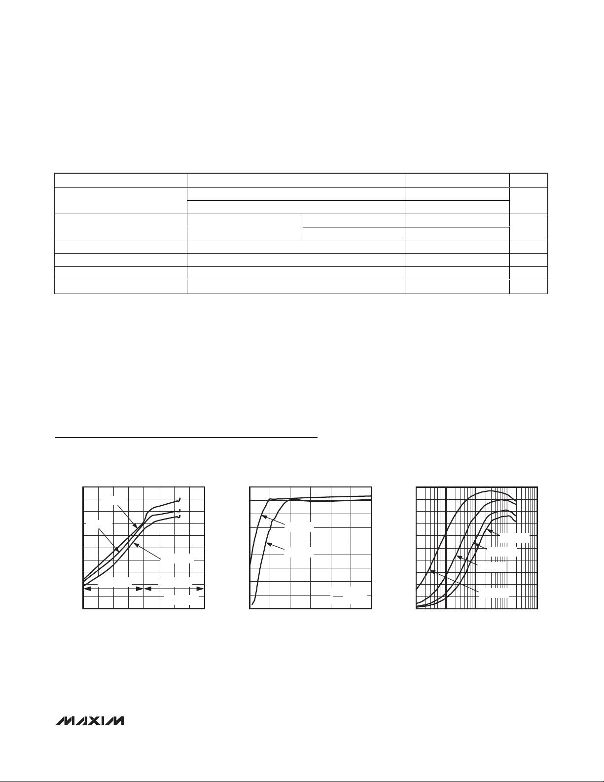
BATTERY CHARGER EFFICIENCY
vs. BATTERY VOLTAGE
100
90
80
70
60
50
40
EFFICIENCY (%)
30
20
10
0
VDC = 5V
VDC = 8V
VDC = 12V
I
= 0.15A
BATT
1.0 2.0 2.51.5 3.0 3.5 4.0 4.5 5.0
BATTERY VOLTAGE (V)
I
BATT
I
BATT
= 1.5A
= 1.5A
4.5
4.0
MAX8903A toc01
3.5
3.0
2.5
2.0
1.5
1.0
SWITCHING FREQUENCY (MHz)
0.5
0.0
486 10121416
SWITCHING FREQUENCY
vs. V
DC
V
= 3V
BAT
V
= 4V
BAT
R
ISET
CEN = 0V
DC VOLTAGE (V)
= 1.2kΩ
100
MAX8903A toc02
SYS EFFICIENCY (%)
SYS EFFICIENCY vs. DC VOLTAGE
90
80
70
60
50
40
30
20
10
0
1 10,000
SYS OUTPUT CURRENT (mA)
VDC = 16V
VDC = 11V
VDC = 6V
VDC = 4.5V
100010010
MAX8903A toc03
Page 6
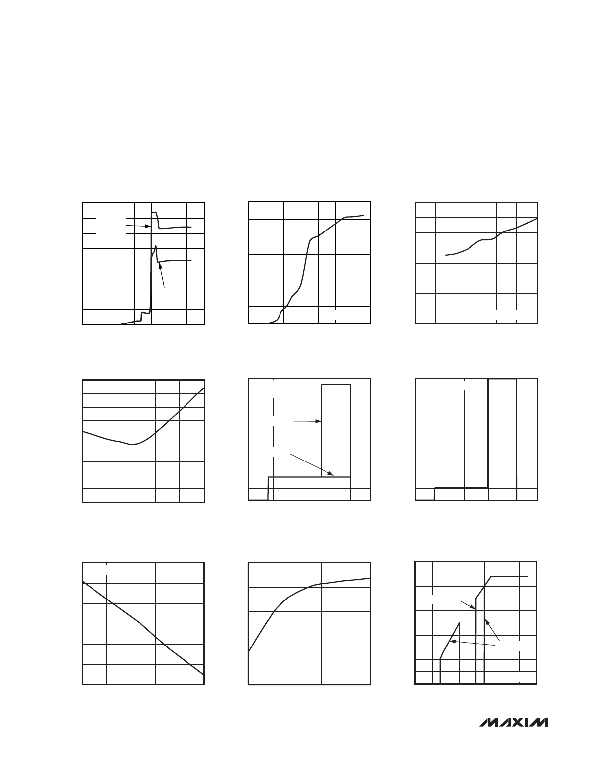
MAX8903A
2A 1-Cell Li+ DC-DC Charger for USB*
and Adapter Power
6 _______________________________________________________________________________________
Typical Operating Characteristics (continued)
(TA = +25°C, unless otherwise noted.)
0
0.4
0.2
0.8
0.6
1.4
1.2
1.0
1.6
021 34567
USB QUIESCENT CURRENT
vs. USB VOLTAGE
MAX8903A toc04
USB VOLTAGE (V)
USB QUIESCENT CURRENT (mA)
CHARGER
ENABLED
CHARGER
DISABLED
0
40
20
80
60
120
100
140
0231 4567
USB QUIESCENT CURRENT
vs. USB VOLTAGE
MAX8903A toc05
USB VOLTAGE (V)
USB QUIESCENT CURRENT (μA)
USB SUSPEND
0
1.5
1.0
0.5
2.5
2.0
4.5
4.0
3.5
3.0
5.0
01234567
SYS VOLTAGE vs. USB VOLTAGE
MAX8903A toc12
USB VOLTAGE (V)
SYS VOLTAGE (V)
V
USB
FALLING
V
USB
RISING
R
SYS
= 1MΩ
80
70
60
50
40
30
20
BATTERY LEAKAGE CURRENT (nA)
10
BATTERY LEAKAGE CURRENT
vs. BATTERY VOLTAGE
MAX8903A toc06
USB UNCONNECTED
0
0456321
BATTERY VOLTAGE (V)
BATTERY LEAKAGE CURRENT
vs. AMBIENT TEMPERATURE
90
80
70
60
50
40
30
20
BATTERY LEAKAGE CURRENT (nA)
10
0
-40 35 60-15 10 85
NORMALIZED CHARGE CURRENT
vs. AMBIENT TEMPERATURE
1.015
V
= 5V, V
USB
1.010
1.005
1.000
0.995
NORMALIZED CHARGE CURRENT
0.990
0.985
-40 85
TEMPERATURE (°C)
= 4V
BATT
TEMPERATURE (°C)
CHARGE CURRENT
vs. BATTERY VOLTAGE—DC MODE
SET TO 1.5A
BAT
SET TO 1A
DC
BATTERY VOLTAGE (V)
MAX8903A toc09
500
450
400
MAX8903A toc07
350
300
250
200
150
CHARGE CURRENT (mA)
100
50
0
CHARGE CURRENT
vs. BATTERY VOLTAGE—USB
CHARGER ENABLED
SET TO 1.5A
I
BAT
V
= V
IUSB
USB
V
= 0V
IUSB
042135
BATTERY VOLTAGE (V)
1000
900
800
MAX8903A toc08
700
600
500
400
300
CHARGE CURRENT (mA)
200
100
0
CHARGER ENABLED
I
I
042315
BATTERY REGULATION VOLTAGE
vs. AMBIENT TEMPERATURE
4.205
4.200
MAX8903A toc10
4.195
4.190
4.185
BATTERY REGULATION VOLTAGE (V)
4.180
603510-15
-40 85
TEMPERATURE (°C)
603510-15
MAX8903A toc11
Page 7

MAX8903A
2A 1-Cell Li+ DC-DC Charger for USB*
and Adapter Power
_______________________________________________________________________________________ 7
Typical Operating Characteristics (continued)
(TA = +25°C, unless otherwise noted.)
4.355
4.365
4.360
4.375
4.370
4.380
4.385
4.395
4.390
4.400
0 10050 200150 300250 400350 500450
SYS VOLTAGE
vs. SYS OUTPUT CURRENT, USB INPUT
MAX8903A toc15
SYS OUTPUT CURRENT (mA)
SYS VOLTAGE (V)
V
USB
= 5V
0
1
2
3
4
5
6
042 6 8 1012141618
VL VOLTAGE vs. DC VOLTAGE
MAX8903A toc16
DC VOLTAGE (V)
VL VOLTAGE (V)
DC SWITCHING
WAVEFORMS—HEAVY LOAD
MAX8903A toc20
200ns/div
V
LX
V
OUT
I
LX
5V/div
0V
20mV/div
AC-COUPLED
500mA/div
0A
R
SYS
= 5Ω
SYS VOLTAGE
vs. DC VOLTAGE
5.0
4.5
4.0
3.5
3.0
2.5
2.0
SYS VOLTAGE (V)
1.5
1.0
0.5
0
0 4682 1012141618
VDC RISING
VDC FALLING
DC VOLTAGE (V)
MAX8903A toc13
vs. SYS OUTPUT CURRENT, DC INPUT
4.50
4.40
4.30
4.20
4.10
SYS VOLTAGE (V)
4.00
3.90
3.80
0 0.3 0.50.1 0.7 0.9 1.1 1.3 1.5
CHARGE PROFILE—1400mAh BATTERY
6.0
5.5
5.0
4.5
4.0
3.5
(V)
3.0
BAT
V
2.5
2.0
1.5
1.0
0.5
0
0 140
SYS VOLTAGE
VDC = 5.75V
USB AND DC UNCONNECTED
= 4V
V
BATT
SYS OUTPUT CURRENT (A)
ADAPTER INPUT—1A CHARGE
IDC SET TO 1A
SET TO 2A
I
BAT
I
BAT
TIME (min)
V
MAX8903A toc17
BAT
MAX8903A toc14
CHARGE PROFILE—1400mAh BATTERY
USB INPUT—500mA CHARGE
1.2
1.0
0.8
0.6
0.4
0.2
0.0
12010060 804020
5.0
4.5
4.0
3.5
3.0
(V)
(A)
2.5
BAT
BAT
I
V
2.0
1.5
1.0
0.5
0
0 200
V
BAT
I
SET TO 500mA
USB
SET TO 2A
I
BAT
TIME (min)
I
MAX8903A toc18
BAT
180160120 14040 60 80 10020
0.500
0.450
0.400
0.350
0.300
(A)
0.250
BAT
I
0.200
0.150
0.100
0.050
0
V
OUT
V
DC SWITCHING WAVEFORMS—LIGHT LOAD
LX
I
LX
200ns/div
MAX8903A toc19
R
SYS
= 44Ω
20mV/div
AC-COUPLED
5V/div
0V
500mA/div
0A
Page 8

MAX8903A
2A 1-Cell Li+ DC-DC Charger for USB*
and Adapter Power
8 _______________________________________________________________________________________
Typical Operating Characteristics (continued)
(TA = +25°C, unless otherwise noted.)
400μs/div
DC CONNECT WITH NO USB
(R
SYS
= 25Ω)
2V/div
MAX8903A toc22
5V/div
1A/div
1A/div
3.6V
3.84V
3.6V
3.44V
C
DC
CHARGING
C
SYS
CHARGING
850mA
-1A
BATTERY
CHARGER
SOFT-START
144mA
0A
V
SYS
V
BAT
I
DC
I
BAT
-I
BAT
= CHARGING
40μs/div
DC DISCONNECT WITH NO USB
(R
SYS
= 25Ω)
2V/div
MAX8903A toc23
5V/div
1A/div
1A/div
3.6V
3.68V
850mA
-1A
144mA
0A
V
SYS
V
BAT
I
DC
I
BAT
3.6V
-I
BAT
= CHARGING
100μs/div
USB DISCONNECT WITH NO DC
(R
SYS
= 25Ω)
2V/div
MAX8903A toc26
5V/div
500mA/div
500mA/div
3.6V
475mA
V
SYS
V
USB
I
USB
I
BAT
5V
144mA
-330mA
DC CONNECT WITH
USB CONNECTED (R
SYS
= 25Ω)
MAX8903A toc21
3.6V
V
SYS
I
DC
475mA
I
USB
-I
BAT
I
-335mA
BAT
200μs/div
SYS LOAD TRANSIENT
(0 TO 1A)
V
SYS
I
SYS
100µs/div
347mA
= CHARGING
MAX8903A toc24
2V/div
500mA/div
500mA/div
0A
500mA/div
50mV/div
AC COUPLED
500mA/div
0A
USB CONNECT WITH NO DC
(R
= 25Ω)
SYS
144mA
3.6V
C
CHARGING
3.5V
USB
BATTERY
CHARGER
SOFT-START
400μs/div
V
SYS
V
USB
I
USB
I
BAT
3.75V
5V
475mA
MAX8903A toc25
2V/div
5V/div
500mA/div
500mA/div
-330mA
V
USUS
V
I
USB
SYS
I
BAT
0V
475mA
3.7V
-475mA
USB SUSPEND
3V
0A
0A
200μs/div
MAX8903A toc27
5V/div
500mA/div
2V/div
500mA/div
V
USUS
I
USB
V
SYS
I
BAT
3V
0A
3.6V
0A
C
USB
CHARGING
BATTERY
CHARGER
SOFT-START
USB RESUME
0V
3.8V
200μs/div
MAX8903A toc28
475mA
3.6V
-475mA
5V/div
500mA/div
2V/div
500mA/div
Page 9

MAX8903A
2A 1-Cell Li+ DC-DC Charger for USB*
and Adapter Power
_______________________________________________________________________________________ 9
Pin Description
PIN NAME FUNCTION
1, 2 PG
3, 4 DC
5 DCM
6 BST High-Side MOSFET Driver Supply. Bypass BST to LX with a 0.1µF ceramic capacitor.
7 IUSB
8 DOK
9VL
10 CT
11 IDC
12 GND Ground. GND is the low-noise ground connection for the internal circuitry.
13 ISET
14 CEN
15 USUS
Power Ground for Step-Down Low-Side Synchronous n-Channel MOSFET. Both PG pins must be
connected together externally.
DC Power Input. DC is capable of delivering up to 2A to SYS. DC supports both AC adapter and USB
inputs. The DC current limit is set through DCM, IUSB, or IDC depending on the input source used. See
Table 2. Both DC pins must be connected together externally. Connect at least a 4.7µF ceramic capacitor
from DC to PG.
Current-Limit Mode Setting for the DC Power Input. When logic-high, the DC input current limit is set by
the resistor at IDC. When logic-low, the DC input current limit is internally programmed to 500mA or
100mA, as set by the IUSB pin.
USB Current-Limit Set Input. Drive IUSB logic-low to set the USB current limit to 100mA. Drive IUSB logichigh to set the USB current limit to 500mA.
DC Power-OK Output. Active-low open-drain output pulls low when a valid input is detected at DC. DOK
is still valid when the charger is disabled (CEN high).
Logic LDO Output. VL is the output of an LDO that powers the MAX8903A internal circuitry and charges
the BST capacitor. Connect a 1µF ceramic capacitor from VL to GND.
Charge Timer Set Input. A capacitor (C
Connect to GND to disable the timer.
DC Current-Limit Set Input. Connect a resistor (R
step-down regulator from 0.5A to 2A when DCM is logic-high.
Charge Current Set Input. A resistor (R
The prequal charge current is 10% of the fast-charge current.
Charger Enable Input. Connect CEN to GND to enable battery charging when a valid source is connected
at DC or USB. Connect to VL, or drive high to disable battery charging.
USB Suspend Input. Drive USUS logic-high to enter USB suspend mode, lowering USB current to 115µA,
and internally shorting SYS to BAT.
) from CT to GND sets the fast-charge and prequal fault timers.
CT
) from IDC to GND to program the current limit of the
IDC
) from ISET to GND programs the fast-charge current up to 2A.
ISET
16 THM
17 USB
18 FLT
19 UOK
20, 21 BAT
Thermistor Input. Connect a negative temperature coefficient (NTC) thermistor from THM to GND.
Connect a resistor equal to the thermistor +25°C resistance from THM to VL. Charging is suspended
when the thermistor is outside the hot and cold limits. Connect THM to GND to disable the thermistor
temperature sensor.
USB Power Input. USB is capable of delivering 100mA or 500mA to SYS as set by the IUSB logic input.
Connect a 4.7µF ceramic capacitor from USB to GND.
Fault Output. Active-low, open-drain output pulls low when the battery timer expires before prequal or
fast-charge completes.
USB Power-OK Output. Active-low, open-drain output pulls low when a valid input is detected at USB.
UOK is still valid when the charger is disabled (CEN high).
Battery Connection. Connect to a single-cell Li+ battery. The battery charges from SYS when a valid
source is present at DC or USB. BAT powers SYS when neither DC nor USB power is present, or when the
SYS load exceeds the input current limit. Both BAT pins must be connected together externally.
Page 10

MAX8903A
2A 1-Cell Li+ DC-DC Charger for USB*
and Adapter Power
10 ______________________________________________________________________________________
Pin Description (continued)
PIN NAME FUNCTION
22 CHG
23, 24 SYS
25, 26 CS
Charger Status Output. Active-low, open-drain output pulls low when the battery is in fast-charge or
prequal. Otherwise, CHG is high impedance.
System Supply Output. SYS connects to BAT through an internal 50mΩ system load switch when DC or
USB are invalid, or when the SYS load is greater than the input current limit.
When a valid voltage is present at DC or USB, SYS is limited to 4.4V. When the system load (I
exceeds the DC or USB current limit, SYS is regulated to 50mV below BAT, and both the powered input
and the battery service SYS.
Bypass SYS to GND with a 10µF X5R or X7R ceramic capacitor. Both SYS pins must be connected
together externally.
70mΩ Current-Sense Input. Connect the step-down inductor from LX to CS. When the step-down
regulator is on, there is a 70mΩ current-sense MOSFET from CS to SYS. When the step-down regulator is
off, the internal CS MOSFET turns off to block current from SYS back to DC.
SYS
)
27, 28 LX
—EP
Inductor Connection. Connect the inductor between LX and CS. Both LX pins must be connected together
externally.
Exposed Pad. Connect the exposed pad to GND. Connecting the exposed pad does not remove the
requirement for proper ground connections to the appropriate pins.
Page 11

2A 1-Cell Li+ DC-DC Charger for USB*
and Adapter Power
MAX8903A
ADAPTER
USB
PG
DC POWER
EMENT
MANAG
DOK
USB
UOK
DC
PWR
OK
STEP-DOWN
REGULA
USB POWER
EMENT
MANAG
PWR
OK
CURRENT-
REGULATOR
AC
LX
PWM
TOR
SET
INPUT
LIMIT
LIMITED
VOLTAGE
SET
INPUT
LIMIT
BST
CS
IC
THERMAL
REGULATION
MAX8903A
Li+ BATTERY
CHARGER
AND SYS LOAD SWITCH
CHARGER
CURRENT-
VOLTAGE
CONTROL
THERMISTOR
MONITOR
(SEE FIGURE 7)
CHARGE
TERMINATION
AND MONITOR
SYS
ISET
BAT
THM
VL
CHG
TO
SYSTEM
LOAD
BATTERY
CONNECTOR
BAT+
BAT-
NTC
+
T
USB
SUSPEND
DC
LIMIT
DCM
IUSB
USUS
IDC
USB
LIMIT
DC MODE
500mA
100mA
Figure 1. Functional Block Diagram
______________________________________________________________________________________ 11
INPUT AND
CHARGER
CURRENT-LIMIT
SET LOGIC
FLT
CHARGE
TIMER
EP
CT
CEN
GND
Page 12

MAX8903A
2A 1-Cell Li+ DC-DC Charger for USB*
and Adapter Power
12 ______________________________________________________________________________________
Circuit Description
The MAX8903A is a dual input charger with a 16V input
for a wide range of DC sources and USB inputs. The IC
includes a high-voltage (16V) input DC-DC step-down
converter that reduces charger power dissipation while
also supplying power to the system load. The stepdown converter supplies up to 2A to the system, the
battery, or a combination of both.
A USB charge input can charge the battery and power
the system from a USB power source. When powered
from USB or the DC input, system load current peaks
that exceed what can be supplied by the input are supplemented by the battery.
The MAX8903A also manages load switching from the
battery to and from an external power source with an
on-chip 50mΩ MOSFET. This switch also helps support
load peaks using battery power when the input source
is overloaded.
Figure 2. Typical Application Circuit Using a Separate DC and USB Connector
R
PU
4 x 100kΩ
1
PG
2
ADAPTER
USB
VBUS
GND
C
4.7μF
C
0.1μF
L1
1μH
DC
BST
C
USB
4.7μF
PG
3
DC
DC
4
6
BST
LX
27
LX
28
CS
25
CS
26
17 USB
MAX8903A
FLT
UOK
DOK
CHG
ISET
IDC
SYS
SYS
BAT
BAT
18
19
8
22
R
ISET
13
R
IDC
11
24
C
23
21
20
10μF
C
BAT
10μF
SYS
TO VL
FAULT
OUTPUT
USB PWR OK
DC PWR OK
CHARGE
INDICATOR
TO SYSTEM
LOAD
1-CELL
LI+
5
OFF
CHARGE ON
500mA
100mA
USB SUSPEND
C
0.15μF
TO VL
CT
DCM
14
CEN
7
IUSB
15
USUS
10
CT
THM
GND
9
VL
RT
16
12
10kΩ
NTC
10kΩ
Page 13

MAX8903A
2A 1-Cell Li+ DC-DC Charger for USB*
and Adapter Power
______________________________________________________________________________________ 13
The IC includes a full-featured charger with thermistor
monitor, fault timer, charger status, and fault outputs.
Also included are power-OK signals for both USB and
DC. Flexibility is maintained with adjustable charge
current, input current limit, and a minimum system voltage (when charging is scaled back to hold the system
voltage up).
The MAX8903A prevents overheating during high ambient temperatures by limiting charging current when the
die temperature exceeds +100°C.
DC Input—Fast Hysteretic
Step-Down Regulator
If a valid DC input is present, the USB power path is
turned off and power for SYS and battery charging is
supplied by the high-frequency step-down regulator
from DC. If the battery voltage is above the minimum
system voltage (V
SYSMIN
, Figure 4), the battery charger
connects the system voltage to the battery for lowest
power dissipation. The step-down regulation point is
then controlled by three feedback signals: maximum
Figure 3. Typical Application Circuit Using a Mini 5 Style Connector or Other DC/USB Common Connector
SERIES
MINI-B
VBUS
GND
D-
D+
ID
4.7μF
TO SYSTEM LOGIC
OFF
CHARGE ON
500mA
100mA
USB SUSPEND
C
DC
C
BST
0.1μF
L1
1μH
0.15μF
R
PU
4 x 100kΩ
1
PG
2
PG
MAX8903A
3
DC
DC
4
6
BST
LX
27
LX
28
CS
25
CS
26
17 USB
5
DCM
14
CEN
7
IUSB
15
USUS
10
C
CT
CT
FLT
UOK
DOK
CHG
ISET
SYS
SYS
BAT
BAT
THM
GND
IDC
18
19
8
22
R
ISET
13
R
IDC
11
24
C
C
1μF
SYS
10μF
C
BAT
10μF
VL
23
21
20
9
VL
16
12
RT
10kΩ
NTC
10kΩ
TO VL
FAULT
OUTPUT
USB PWR OK
DC PWR OK
CHARGE
INDICATOR
TO SYSTEM
LOAD
1-CELL
LI+
Page 14

MAX8903A
2A 1-Cell Li+ DC-DC Charger for USB*
and Adapter Power
14 ______________________________________________________________________________________
step-down output current programmed at IDC, maximum charger current programmed at ISET, and maximum die temperature. The feedback signal requiring
the smallest current controls the average output current
in the inductor. This scheme minimizes total power dissipation for battery charging and allows the battery to
absorb any load transients with minimum system voltage disturbance.
If the battery voltage is below V
SYSMIN
, the charger
does not directly connect the system voltage to the battery. V
SYS
pin is held at a fixed point slightly above
V
SYSMIN
, and does not track the battery. The battery
charger independently controls the battery charging
current. V
SYSMIN
is set to 3.0V in the MAX8903A, for
other V
SYSMIN
values, please contact the factory.
After the battery charges to 50mV above V
SYSMIN
, the
system voltage is connected to the battery. The battery
fast-charge current then controls the step-down converter to set the average inductor current so that both
the programmed input current limit and fast-charge current limit are satisfied.
DC-DC Step-Down Control Scheme
A proprietary hysteretic current PWM control scheme
ensures fast switching and physically tiny external components. The feedback control signal that requires the
smallest input current controls the center of the peak
and valley currents in the inductor. The ripple current is
internally set to provide 4MHz operation. When the
input voltage decreases near the output voltage, very
high duty cycle occurs and, due to minimum off-time,
4MHz operation is not achievable. The controller then
provides minimum off-time, peak current regulation.
Similarly, when the input voltage is too high to allow
4MHz operation due to the minimum on-time, the controller becomes a minimum on-time, valley current regulator. In this way, ripple current in the inductor is always
as small as possible to reduce ripple voltage on SYS for
a given capacitance. The ripple current is made to vary
with input voltage and output voltage in a way that
reduces frequency variation. However, the frequency
still varies somewhat with operating conditions. See the
Typical Operating Characteristics
.
DC Input—USB mode
When powering from DC with DCM set to logic-low, the
DC input is set to USB mode. The input current limit from
DC is then internally set to 500mA max if IUSB is high
and 100mA max if IUSB is low. For the 500mA case, the
DC input continues to operate as a step-down regulator
to minimize thermal heating. For the 100mA case, the
Table 1. External Components List for Figures 2 and 3
Figure 4. SYS Tracking V
BAT
to the Minimum System Voltage
COMPONENT
(FIGURES 2 AND 3)
CDC, C
USB
C
VL
C
SYS
C
BAT
C
CT
RPU (X4) Logic output pullup resistors 100kΩ
THM Negative TC thermistor
R
T
R
IDC
R
ISET
L1 DC input step-down inductor 1µH inductor with I
Input filter capacitor 4.7µF ceramic capacitor
VL filter capacitor 1.0µF ceramic capacitor
SYS output bypass capacitor 10µF ceramic capacitor
Battery bypass capacitor 10µF ceramic capacitor
Charger timing capacitor 0.15µF low TC ceramic capacitor
THM pullup resistor 10kΩ
DC input current-limit programming resistor 3kΩ ±1%, for 2A limit
Fast-charge current programming resistor 1.2kΩ ±1%, for 1A charging
FUNCTION PART
Phillips NTC thermistor, P/N 2322-640-63103, 0kΩ
±5% at +25°C
SAT
> 2A
4.4V
4.2V
V
SYS
I
x R
BAT
V
SYSMIN
V
BAT
ON
Page 15

MAX8903A
2A 1-Cell Li+ DC-DC Charger for USB*
and Adapter Power
______________________________________________________________________________________ 15
step-down regulator is turned off and a low-dropout linear regulator is connected between DC and SYS.
USB Input—Linear Regulator
If a valid USB input is present with no valid DC input,
current for SYS and battery charging is supplied by a
low-dropout linear regulator connected from USB to
SYS. The SYS regulation voltage shows the same characteristic as when powering from the DC input (see
Figure 4). The battery charger operates from SYS with
any extra available current, while not exceeding the
maximum-allowed USB current. If both USB and DC
inputs are valid, power is only taken from the DC input.
The maximum USB input current is set by the logic
state of the IUSB input to either 100mA or 500mA.
Power Monitor Outputs (
UOK, DOK
)
DOK is an open-drain, active-low output that indicates
the DC input power status. With no source at the USB
pin, the source at DC is considered valid and DOK is
driven low when: 4.15V < VDC< 16V. When the USB
voltage is also valid, the DC source is considered valid
and DOK is driven low when: 4.45V < VDC< 16V. The
higher minimum DC voltage with USB present helps
guarantee cleaner transitions between input supplies. If
the DC power-OK output feature is not required, connect DOK to ground.
UOK is an open-drain, active-low output that indicates
the USB input power status. UOK is low when a valid
source is connected at USB. The source at USB is valid
when 4.1V < V
USB
< 6.6V. If the USB power-OK output
feature is not required, connect UOK to ground.
Both the UOK and the DOK circuitry remain active in
thermal overload, USB suspend, and when the charger
is disabled. DOK and UOK can also be wire-ORed
together to generate a single power-OK (POK) output.
Thermal Limiting
When the die temperature exceeds +100°C, a thermal
limiting circuit reduces the input current limit by 5%/°C,
bringing the charge current to 0mA at +120°C. Since
the system load gets priority over battery charging, the
battery charge current is reduced to 0mA before the
input limiter drops the load voltage at SYS. To avoid
false charge termination, the charge termination detect
function is disabled in this mode. If the junction temperature rises beyond +120°C, no current is drawn from
DC or USB, and V
SYS
regulates at 50mV below V
BAT
.
System Voltage Switching
DC Input
When charging from the DC input, if the battery is
above the minimum system voltage, SYS is connected
to the battery. Current is provided to both SYS and the
battery, up to the maximum program value. The stepdown output current sense and the charger current
sense provide feedback to ensure the current loop
demanding the lower input current is satisfied. The
advantage of this approach when powering from DC is
that power dissipation is dominated by the step-down
regulator efficiency, since there is only a small voltage
drop from SYS to BAT. Also, load transients can be
absorbed by the battery while minimizing the voltage
disturbance on SYS. If both the DC and USB inputs are
valid, the DC input takes priority and delivers the input
current, while the USB input is off.
After the battery is done charging, the charger is turned
off and the SYS load current is supplied from the DC
input. The SYS voltage is regulated to 4.4V. The charger turns on again after the battery drops to the restart
threshold. If the load current exceeds the input limiter,
SYS drops down to the battery voltage and the 50mΩ
SYS-to-BAT PMOS switch turns on to supply the extra
load current. The SYS-to-BAT switch turns off again
once the load is below the input current limit. The 50mΩ
PMOS also turns on if valid DC input power is removed.
USB Input
When charging from the USB input, the DC input stepdown regulator turns off and a linear regulator from
USB to SYS powers the system and charges the battery. If the battery is greater than the minimum system
voltage, the SYS voltage is connected to the battery.
The USB input then supplies the SYS load and charges
the battery with any extra available current, while not
exceeding the maximum-allowed USB current. Load
transients can be absorbed by the battery while minimizing the voltage disturbance on SYS. When battery
charging is completed, or the charger is disabled, SYS
is regulated to 4.4V. If both USB and DC inputs are
valid, power is only taken from the DC input.
USB Suspend
Driving USUS high turns off charging as well as the SYS
output and reduces input current to 170µA to accommodate USB suspend mode.
Charge Enable (
CEN
)
When CEN is low, the charger is on. When CEN is high,
the charger turns off. CEN does not affect the SYS output. In many systems, there is no need for the system
controller (typically a microprocessor) to disable the
charger, because the MAX8903A smart power selector
circuitry independently manages charging and
adapter/battery power hand-off. In these situations,
CEN may be connected to ground.
Page 16

MAX8903A
2A 1-Cell Li+ DC-DC Charger for USB*
and Adapter Power
16 ______________________________________________________________________________________
Soft-Start
To prevent input transients that can cause instability in
the USB or AC adapter power source, the rate of
change of the input current and charge current is limited. When an input source is valid, SYS current is
ramped from zero to the set current-limit value in typically 50µs. This also means that if DC becomes valid
after USB, the SYS current limit is ramped down to zero
before switching from the USB to DC input. At some
point, SYS is no longer able to support the load and
may switch over to BAT. The switchover to BAT occurs
when V
SYS
< V
BATT
. This threshold is a function of the
SYS capacitor size and SYS load. The SYS current limit
then ramps from zero to the set current level and SYS
supports the load again as long as the SYS load current
is less than the set current limit.
When the charger is turned on, the charge current ramps
from 0A to the ISET current value in typically 1.0ms.
Charge current also soft-starts when transitioning to fastcharge from prequal, when the input power source is
switched between USB and DC, and when changing the
USB charge current from 100mA to 500mA with the IUSB
logic input. There is no di/dt limiting, however, if R
ISET
is
changed suddenly using a switch.
Battery Charger
While a valid input source is present, the battery charger can attempt to charge the battery with a fast-charge
current determined by the resistance at the ISET pin:
R
ISET
= 1200/I
CHG-MAX
Monitoring Charge Current
The voltage from ISET to GND is a representation of the
battery charge current and can be used to monitor the
current charging the battery. A voltage of 1.5V represents the maximum fast-charge current.
If necessary, the charge current is reduced automatically to prevent the SYS voltage from dropping.
Therefore, a battery never charges at a rate beyond the
capabilities of a 100mA or 500mA USB input, or overloads an AC adapter. See Figure 5.
Table 2. Input Limiter Control Logic
**
Charge current cannot exceed the input current limit. Charge may be less than the maximum charge current if the total SYS load
exceeds the input current limit.
X = Don’t care.
DC STEP-DOWN
POWER SOURCE DOK UOK DCM IUSB USUS
AC Adapter at DC Input L X H X X 6000/R
OUTPUT
CURRENT LIMIT
IDC
USB INPUT
CURRENT LIMIT
MAXIMUM
CHARGE
CURRENT**
Lesser of
1200/R
ISET
6000/R
and
IDC
USB Power at DC Input
USB Power at USB Input,
DC Unconnected
DC and USB Unconnected H H X X X
L X L L L 100mA
L X L H L 500mA
L X L X H USB suspend
H L X L L 100mA
H L X H L 500mA
H L X X H USB suspend 0
No DC input
USB input off. DC
input has priority.
No USB input 0
1200/R
1200/R
1200/R
1200/R
Lesser of
ISET
100mA
Lesser of
ISET
500mA
0
Lesser of
ISET
100mA
Lesser of
ISET
500mA
and
and
and
and
Page 17

MAX8903A
2A 1-Cell Li+ DC-DC Charger for USB*
and Adapter Power
______________________________________________________________________________________ 17
When V
BATT
is below 3V, the charger enters prequal
mode and the battery charges at 10% of the maximum
fast-charge rate until the voltage of the deeply discharged battery recovers. When the battery voltage
reaches 4.2V and the charge current drops to 10% of
the maximum fast-charge current, the charger enters
the DONE state. The charger restarts a fast-charge
cycle if the battery voltage drops by 100mV.
Charge Termination
When the charge current falls to the termination threshold (I
TERM
) and the charger is in voltage mode, charging is complete. Charging continues for a brief 15s
top-off period and then enters the DONE state where
charging stops.
Note that if charge current falls to I
TERM
as a result of
the input or thermal limiter, the charger does not enter
DONE. For the charger to enter DONE, charge current
must be less than I
TERM
, the charger must be in voltage mode, and the input or thermal limiter must not be
reducing charge current.
Charge Status Outputs
Charge Output (CHG)
CHG is an open-drain, active-low output that indicates
charger status. CHG is low when the battery charger is
in its prequalification and fast-charge states. CHG goes
high impedance if the thermistor causes the charger to
go into temperature suspend mode.
When used in conjunction with a microprocessor (µP),
connect a pullup resistor between CHG and the logic
I/O voltage to indicate charge status to the µP.
Alternatively, CHG can sink up to 20mA for an LED
charge indicator.
Fault Output (FLT)
FLT is an open-drain, active-low output that indicates
charger status. FLT is low when the battery charger has
entered a fault state when the charge timer expires.
This can occur when the charger remains in its prequal
state for more than 33 minutes or if the charger remains
in fast-charge state for more than 660 minutes (see
Figure 6). To exit this fault state, toggle CEN or remove
and reconnect the input source.
When used in conjunction with a microprocessor (µP),
connect a pullup resistor between FLT and the logic I/O
voltage to indicate charge status to the µP.
Alternatively, FLT can sink up to 20mA for an LED fault
indicator. If the FLT output is not required, connect FLT
to ground or leave unconnected.
Charge Timer
A fault timer prevents the battery from charging indefinitely. The fault prequal and fast-charge timers are controlled by the capacitance at CT (CCT).
While in fast-charge mode, a large system load or device
self-heating may cause the MAX8903A to reduce charge
current. Under these circumstances, the fast-charge
timer is slowed by 2x if the charge current drops below
50% of the programmed fast-charge level, and suspended if the charge current drops below 20% of the programmed level. The fast-charge timer is not affected at
any current if the charger is regulating the BAT voltage
at 4.2V (i.e., the charger is in voltage mode).
Thermistor Input (THM)
The THM input connects to an external negative temperature coefficient (NTC) thermistor to monitor battery
or system temperature. Charging is suspended when
the thermistor temperature is out of range. The charge
timers are suspended and hold their state but no fault is
indicated. When the thermistor comes back into range,
Figure 5. Monitoring the Battery Charge Current with the
Voltage from ISET to GND
MONITORING THE BATTERY
CHARGE CURRENT WITH V
1.5
(V)
V
ISET
0
DISCHARGING
0
BATTERY CHARGING CURRENT (A)
ISET
1200/R
ISET
C
t
PREQUAL
t
FST CHG
−
ts
TOP OFF
−
min
=×
33
min
660
=×
15
=
CT
.
015
C
.μμ
015
F
CT
F
Page 18

MAX8903A
2A 1-Cell Li+ DC-DC Charger for USB*
and Adapter Power
18 ______________________________________________________________________________________
charging resumes and the charge timer continues from
where it left off. Connecting THM to GND disables the
thermistor monitoring function. Table 4 lists the fault
temperature of different thermistors.
Since the thermistor monitoring circuit employs an
external bias resistor from THM to VL (R
TB
, Figure 7),
the thermistor is not limited only to 10kΩ (at +25°C).
Any resistance thermistor can be used as long as the
value is equivalent to the thermistor’s +25°C resistance.
For example, with a 10kΩ at +25°C thermistor, use
10kΩ at R
TB
, and with a 100kΩ at +25°C thermistor,
use 100kΩ .
For a typical 10kΩ (at +25°C) thermistor and a 10kΩ
RTBresistor, the charger enters a temperature suspend
Figure 6. MAX8903A Charger State Flow Chart
V
< 2.8V
BATT
RESET TIMER
ANY CHARGING
STAT E
THM OK
TIMER RESUME
TEMPERATURE SUSPEND
UOK OR DOK PREVIOUS STATE
= 0mA
I
CHG
CHG = HIGH IMPEDANCE
FLT = HIGH IMPEDANCE
THM NOT OK
TIMER SUSPEND
NOT READY
UOK AND DOK = HIGH IMPEDANCE
CHG = HIGH IMPEDANCE
FLT = HIGH IMPEDANCE
= 0mA
I
CHG
PREQUALIFICATION
UOK AND/OR DOK = LOW
CHG = LOW
FLT = HIGH IMPEDANCE
0 < V
BAT
≤ I
I
CHG
CHGMAX
V
< 2.82V
BATT
RESET TIMER = 0
FAST-CHARGE
UOK AND/OR DOK = LOW
CHG = LOW
FLT = HIGH IMPEDANCE
3V < V
BAT
≤ I
I
CHG
CHGMAX
> I
I
CHG
TERM
RESET TIMER
TOP-OFF
UOK AND/OR DOK = LOW
CHG = HIGH IMPEDANCE
FLT = HIGH IMPEDANCE
VBAT = 4.2V
= I
I
CHG
DONE
UOK AND/OR DOK = 0
CHG = HIGH IMPEDANCE
FLT = HIGH IMPEDANCE
4.1V < V
BAT
= 0mA
I
CHG
UOK AND/OR DOK = LOW
CEN = 0
RESET TIMER
< 3V
/10
V
> 3.0V
BATT
RESET TIMER
< 4.2V
I
CHG
AND V
AND THERMAL
OR INPUT LIMIT
NOT EXCEEDED;
RESET TIMER
TERM
TIMER > 15s
< 4.2V
CEN = HI OR
REMOVE AND RECONNECT
THE INPUT SOURCE(S)
TIMER > t
< I
TERM
= 4.2V
BAT
PREQUAL
V
< 4.1V
BAT
RESET TIMER
ANY STATE
TOGGLE CEN OR
REMOVE AND RECONNECT
THE INPUT SOURCE(S)
FAULT
UOK AND/OR DOK = LOW
CHG = HIGH IMPEDANCE
FLT = LOW
= 0mA
I
CHG
TIMER > t
FSTCHG
(TIMER SLOWED BY 2x IF
< I
CHGMAX
CHG
/2, AND
< I
CHGMAX
I
CHG
PAUSED IF I
/5 WHILE V
BAT
< 4.2V)
Page 19

MAX8903A
2A 1-Cell Li+ DC-DC Charger for USB*
and Adapter Power
______________________________________________________________________________________ 19
state when the thermistor resistance falls below 3.97kΩ
(too hot) or rises above 28.7kΩ (too cold). This corresponds to a 0°C to +50°C range when using a 10kΩ
NTC thermistor with a beta of 3500. The general relation
of thermistor resistance to temperature is defined by
the following equation:
where:
R
T
= The resistance in Ω of the thermistor at tempera-
ture T in Celsius
R25= The resistance in Ω of the thermistor at +25°C
ß = The material constant of the thermistor, which typically ranges from 3000K to 5000K
T = The temperature of the thermistor in °C
Table 4 shows the MAX8903A THM temperature limits
for different thermistor material constants.
Some designs might prefer other thermistor temperature limits. Threshold adjustment can be accommodated by changing RTB, connecting a resistor in series
and/or in parallel with the thermistor, or using a thermistor with different ß. For example, a +45°C hot threshold
and 0°C cold threshold can be realized by using a thermistor with a ß of 4250 and connecting 120kΩ in parallel. Since the thermistor resistance near 0°C is much
higher than it is near +50°C, a large parallel resistance
lowers the cold threshold, while only slightly lowering
the hot threshold. Conversely, a small series resistance
Figure 7. Thermistor Monitor Circuitry
Table 3. Fault Temperatures for Different
Thermistors
CEN
THERMISTOR
CIRCUITRY
VL
VL
MAX8903A
ALTERNATE
THERMISTOR
CONNECTION
RTS
R
T
RTP
RTB
0.74 VL
THM
0.28 VL
R
T
0.03 VL
GND
Thermistor ß (K) 3000 3250 3500 3750 4250
RTB (kΩ) (Figure 7) 10 10 10 10 10
Resistance at +25°C
(kΩ)
Resistance at +50°C
(kΩ)
Resistance at 0°C (kΩ) 25.14 27.15 29.32 31.66 36.91
Nominal Hot Trip
Temperature (°C)
Nominal Cold Trip
Temperature (°C)
10 10 10 10 10
4.59 4.30 4.03 3.78 3316
55 53 50 49 46
-3 -1 0 2 4.5
COLD
THM
OUT OF
RANGE
DISABLE
CHARGER
⎧
β
⎨
25
⎩
RR e
=×
T
⎛
⎜
⎝
T
+
1
−
2731298
⎫
⎞
⎟
⎬
⎠
⎭
ALL COMPARATORS
60mV HYSTERESIS
HOT
ENABLE THM
Page 20

MAX8903A
2A 1-Cell Li+ DC-DC Charger for USB*
and Adapter Power
Maxim cannot assume responsibility for use of any circuitry other than circuitry entirely embodied in a Maxim product. No circuit patent licenses are
implied. Maxim reserves the right to change the circuitry and specifications without notice at any time.
20
____________________Maxim Integrated Products, 120 San Gabriel Drive, Sunnyvale, CA 94086 408-737-7600
© 2008 Maxim Integrated Products is a registered trademark of Maxim Integrated Products, Inc.
raises the cold threshold, while only slightly raising the
hot threshold. Raising RTBlowers both the hot and cold
thresholds, while lowering R
TB
raises both thresholds.
Note that since VL is active whenever valid input power
is connected at DC or USB, thermistor bias current
flows at all times, even when charging is disabled (CEN
= high). When using a 10kΩ thermistor and a 10kΩ
pullup to VL, this results in an additional 250µA load.
This load can be reduced to 25µA by instead using a
100kΩ thermistor and 100kΩ pullup resistor.
Power Dissipation
PCB Layout and Routing
Good design minimizes ground bounce and voltage
gradients in the ground plane, which can result in instability or regulation errors. The GND and PGs should
connect to the power-ground plane at only one point to
minimize the effects of power-ground currents. Battery
ground should connect directly to the power-ground
plane. The ISET and IDC current-setting resistors
should connect directly to GND to avoid current errors.
Connect GND to the exposed pad directly under the IC.
Use multiple tightly spaced vias to the ground plane
under the exposed pad to help cool the IC. Position
input capacitors from DC, SYS, BAT, and USB to the
power-ground plane as close as possible to the IC.
Keep high current traces such as those to DC, SYS,
and BAT as short and wide as possible. Refer to the
MAX8903A Evaluation Kit for a suitable PCB layout
example.
Table 4. Package Thermal Characteristics
Pin Configuration
Chip Information
PROCESS: BiCMOS
Package Information
For the latest package outline information and land patterns, go
to www.maxim-ic.com/packages
.
PACKAGE TYPE PACKAGE CODE DOCUMENT NO.
28 TQFN-EP T2844-1
21-0139
28-PIN 4mm x 4mm THIN QFN
SINGLE-LAYER PCB MULTILAYER PCB
Continuous
Power
Dissipation
θ
JA
θ
JC
1666.7mW
Derate 20.8mW/°C
above +70°C
48°C/W 35°C/W
3°C/W 3°C/W
2286mW
Derate 28.6mW/°C
above +70°C
TOP VIEW
22
CHG
SYS
23
24
SYS
25
26
CS
27
LX
28
LX
*EXPOSED PAD
+
12CS4567
UOK
BAT
FLT
BAT
2021 19 17 16 15
MAX8903A
3
PG
PG
THIN QFN
4mm x 4mm
USB
18
DC
DC
DCM
*EP
THM
BST
USUS
IUSB
14
CEN
ISET
13
12
GND
IDC
11
10
CT
VL
9
8
DOK
 Loading...