

Page 1
General Description
The MAX8902A/MAX8902B low-noise linear regulators
deliver up to 500mA of output current with only
16µV
RMS
of output noise in a 100kHz bandwidth. These
regulators maintain their output voltage over a wide
input range, requiring only 100mV of input-to-output
headroom at full load.
These LDOs maintain a low 80µA typical supply current, independent of the load current and dropout voltage. The regulator control circuitry includes a
programmable soft-start circuit and short circuit,
reverse current, and thermal-overload protection. Other
features include an enable input and a power-OK output (MAX8902B only).
The MAX8902A output voltage can be set to 1.5V, 1.8V,
2.0V, 2.5V, 3.0V, 3.1V, 3.3V, 4.6V, or 4.7V using the
SELA and SELB inputs. The MAX8902B output voltage
can be set between 0.6V and 5.3V with an external
resistor voltage-divider.
Applications
Notebook Computers
MP3 and Portable Media Players
Wireless Headphones
GPS Portable Navigation Devices
Smartphones
Features
♦ 1.7V to 5.5V Input Voltage Range
♦ 0.6V to 5.3V Output Voltage Range
♦ 16µV
RMS
Output Noise, 10Hz to 100kHz
♦ 80µA Operating Supply Current
♦ 92dB PSRR at 5kHz
♦ Guaranteed 500mA Output Current
♦ ±1.5% Output Accuracy Over Load, Line, and
Temperature
♦ 100mV (max) Dropout at 500mA Load
♦ < 1µA Shutdown Supply Current
♦ 700mA Short-Circuit Protection
♦ Thermal-Overload Protection
♦ Output-to-Input Reverse Current Protection
♦ 2mm x 2mm x 0.8mm TDFN Package
MAX8902A/MAX8902B
Low-Noise 500mA LDO Regulators
in a 2mm x 2mm TDFN Package
________________________________________________________________
Maxim Integrated Products
1
19-0990; Rev 2; 2/08
For pricing, delivery, and ordering information, please contact Maxim Direct at 1-888-629-4642,
or visit Maxim's website at www.maxim-ic.com.
EVALUATION KIT
AVAILABLE
Ordering Information
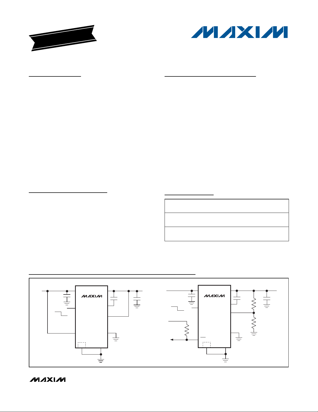
Typical Operating Circuits
+
Denotes a lead-free, RoHS-compliant package.
Note: All devices are in an 8-pin, 2mm x 2mm TDFN package
with an exposed paddle and operate over the -40°C to +125°C
automotive temperature range.
Pin Configurations appear at end of data sheet.
PART FEATURES
MAX8902AATA+
MAX8902BATA+
Pin-selectable output
voltage
Adjustable output
voltage
TOP
MARK
ABG T822-1
ABH T822-1
PKG
CODE
INPUT
4.7V TO 5.5V
10μF
ON
IN
EN
OFF
SELA
EP
OUT
MAX8902A
BYP
OUTS
SELB
GND
0.01μF
OUTPUT
4.6V
10μF
INPUT
1.7V TO 5.5V
ON
LOGIC
SUPPLY
TO μC
10μF
100kΩ
OUTPUT ADJUSTABLE
0.01μF
0.6V TO 5.3V
10μF
R1
R2
IN
MAX8902B
EN
OFF
R3
POK
EP
OUT
BYP
FB
GS
GND
Page 2
MAX8902A/MAX8902B
Low-Noise 500mA LDO Regulators
in a 2mm x 2mm TDFN Package
2 _______________________________________________________________________________________
ABSOLUTE MAXIMUM RATINGS
Stresses beyond those listed under “Absolute Maximum Ratings” may cause permanent damage to the device. These are stress ratings only, and functional
operation of the device at these or any other conditions beyond those indicated in the operational sections of the specifications is not implied. Exposure to
absolute maximum rating conditions for extended periods may affect device reliability.
BYP, EN, IN, OUT, SELA, SELB, POK to GND, GS to GND, FB,
OUTS to GND .....................................................-0.3V to +6.0V
Output Short-Circuit Duration.....................................Continuous
Continuous Power Dissipation (T
A
= +70°C)
8-Pin, 2mm x 2mm TDFN
(derate 11.9mW/°C above +70°C).............................953.5mW
Operating Temperature Range .........................-40°C to +125°C
Junction Temperature Range ............................-40°C to +150°C
Storage Temperature Range .............................-65°C to +150°C
Lead Temperature (soldering, 10s) .................................+300°C
ELECTRICAL CHARACTERISTICS
(VIN= VEN= 5V, OUTS = OUT, circuit of Figure 2 (MAX8902A) and Figure 3 (MAX8902B), TA= -40°C to +125°C, unless otherwise
noted.) (Note 1)
IN
Input Voltage Range 1.7 5.5 V
Input Undervoltage Lockout VIN rising, 100mV typical hysteresis 1.5 1.6 1.7 V
OUT
Output Voltage Range VIN ≥ V
Output Voltage Accuracy
Load Regulation I
Line Regulation
Dropout Voltage
(Note 2)
Current Limit V
Output Noise I
OUTS (MAX8902A only)
OUTS Input Bias Current In regulation 0.5 7.0 µA
FB (MAX8902B only)
FB Threshold Accuracy VIN = 1.7V to 5.5V, I
FB Input Bias Current VFB = 0.6V
BYP
BYP Capacitor Range Regulator remains stable 1 100 nF
BYP Startup Current From BYP to GND during startup 50 µA
PARAMETER CONDITIONS MIN TYP MAX UNITS
+ 0.1V 0.6 5.3 V
OUT
= 1.7V to 5.5V for V
V
IN
= (V
V
IN
I
OUT
OUT
= 1.7V to 5.5V for V
V
IN
= (V
V
IN
I
OUT
I
OUT
OUT
OUT
OUT
+ 0.3V) to 5.5V for V
OUT
= 0.1mA to 500mA
= 0.1mA to 500mA 0.02 %
+ 0.3V) to 5.5V for V
OUT
= 200mA
= 500mA
= 95% of regulation, VIN = V
= 100mA, f = 10Hz to 100kHz, C
= 10mA
OUT
OUT
OUT
≤ 1.4V,
> 1.4V,
OUT
≤ 1.4V,
> 1.4V,
OUT
VIN ≥ 3.6V, TA ≤ +85°C 50 100
VIN ≥ 3.6V, TA ≤ +125°C 120
= 1.7V 150
V
IN
+ 0.5V 600 700 800 mA
OUT
= 0.01µF 16 µV
BYP
f = 5kHz 92
f = 10kHz 85Power-Supply Rejection Ratio I
f = 100kHz 62
= 0.1mA to 500mA 0.591 0.600 0.609 V
TA = +25°C -0.1 0.02 +0.1
T
= -40°C 0.03
A
-1.5 +1.5 %
0.04 %
mV
RMS
dB
µA
Page 3
MAX8902A/MAX8902B
Low-Noise 500mA LDO Regulators
in a 2mm x 2mm TDFN Package
_______________________________________________________________________________________ 3
ELECTRICAL CHARACTERISTICS (continued)
(VIN= VEN= 5V, OUTS = OUT, circuit of Figure 2 (MAX8902A) and Figure 3 (MAX8902B), TA= -40°C to +125°C, unless otherwise
noted.) (Note 1)
Note 1: All devices are production tested at TA= +25°C. Specifications over the operating temperature range are guaranteed by
design and characterization.
Note 2: The dropout voltage is defined V
IN
- V
OUT
, when V
OUT
is 5% lower than the value of V
OUT
when VIN= V
OUT
+ 0.5V.
GND
GND Supply Current I
GND Shutdown Current VIN = 5.5V, EN = 0V
SELA/SELB (MAX8902A only)
Select Input Resistance
Select Input Capacitance When open 10 pF
EN
Enable Input Bias Current VEN = 0V to 5.5V
POK (MAX8902B only)
POK Threshold
POK Voltage, Low I
POK Leakage Current POK = 5.5V, VEN = 0V
THERMAL SHUTDOWN
Thermal Shutdown Threshold
OUTPUT TRANSIENT
Load Transient I
Line Transient VIN = 4V to 5V to 4V, t
IN-to-OUT Reverse Voltage
Turnoff Threshold
PARAMETER CONDITIONS MIN TYP MAX UNITS
= 0mA
OUT
When shorted to GND or V
When open 1 MΩ
OUT voltage when POK
switches
= 1mA 10 100 mV
POK
TJ rising 165
T
falling 150
J
= 50mA to 500mA to 50mA, t
OUT
IN falling below OUT 10 mV
TA < +85°C 80 120
T
< +125°C 160
A
TA = +25°C 0.001 +1
= +85°C 0.01
T
A
IN
EN rising 0.8 1.2
EN falling, TA < +85°C 0.4 0.7Enable Input Threshold VIN = 1.7V to 5.5V
EN falling, T
TA = +25°C -1 0.001 +1
= +85°C 0.01
T
A
OUT rising 88 91 94 %
OUT falling 88 %
TA = +25°C -1 0.001 +1
= +85°C 0.01
T
A
RISE
= t
FALL
= 5µs, I
RISE
< +125°C 0.38 0.7
A
= t
= 1µs 25
FALL
= 500mA 3
OUT
µA
µA
500 Ω
µA
µA
°C
mV/
mV/
V
P-P
P-P
Page 4
MAX8902A/MAX8902B
Low-Noise 500mA LDO Regulators
in a 2mm x 2mm TDFN Package
4 _______________________________________________________________________________________
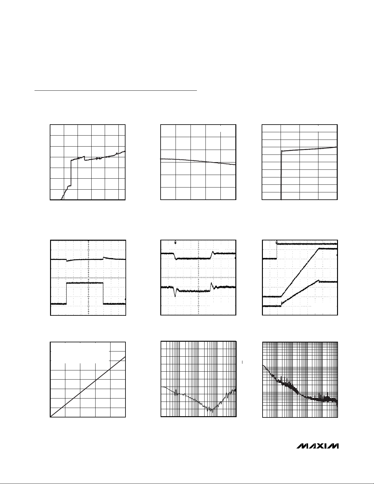
Typical Operating Characteristics
(MAX8902A, VIN= 3.6V, V
OUT
= 2.5V, TA= +25°C, unless otherwise noted.)
0
40
20
80
60
120
100
140
023145
QUIESCENT CURRENT
EN = HIGH, NO LOAD
MAX8902A/02B toc01
INPUT VOLTAGE (V)
INPUT CURRENT (μA)
2.500
2.502
2.501
2.504
2.503
2.505
2.506
0200100 300 400 500
LOAD REGULATION
MAX8902A/02B toc02
LOAD CURRENT (mA)
OUTPUT VOLTAGE (V)
3.6V INPUT
2.490
2.496
2.494
2.492
2.498
2.500
2.502
2.504
2.506
2.508
2.510
1.5 2.5 3.5 4.5 5.5
LINE REGULATION
MAX8902A/02B toc03
INPUT VOLTAGE (V)
OUTPUT VOLTAGE (V)
200mA LOAD
40ms/div
LOAD TRANSIENT RESPONSE
50mA TO 500mA TO 50mA
V
OUT
100mV/div
200mA/div
MAX8902A/02B toc04
I
OUT
t
RISE
= t
FALL
= 1μs
10μs/div
LOAD TRANSIENT RESPONSE
V
IN
2V/div
2mV/div
MAX8902A/02B toc05
V
OUT
2.5V OUTPUT
5Ω LOAD
5V
4V
5V
100μs/div
STARTUP WAVEFORM
V
EN
500mV/div
2V/div
200mA/div
MAX8902A/02B toc06
I
IN
V
OUT
5Ω LOAD
C
BYP
= 0.01μF
0
10
20
30
40
50
60
70
80
0 100 200 300 400 500
DROPOUT VOLTAGE vs. LOAD CURRENT
MAX8902A/02B toc07
LOAD CURRENT (mA)
DROPOUT VOLTAGE (mV)
3.6V INPUT, 4.6V OUTPUT PRESET
THE SLOPE OF THE LINE INDICATES
A 129mΩ ON-RESISTANCE IN
DROPOUT
PSRR vs. FREQUENCY
MAX8902A/02B toc08
10k1k10010 100k
FREQUENCY (Hz)
0
-10
-20
-30
-40
-50
-60
-70
-80
-90
-100
PSRR (dB)
MAX8902A LDO OUTPUT-NOISE SPECTRAL
DENSITY vs. FREQUENCY
MAX8902A/02B toc09
FREQUENCY (Hz)
100k10k1k100
100E+0
1E+3
10E+3
10E+0
10 1M
NOISE DENSITY (nV √Hz)
Page 5

Detailed Description
The MAX8902A/MAX8902B low-noise, low-dropout linear regulators deliver up to 500mA of output current
with only 16µV
RMS
of output noise in a 100kHz bandwidth. These regulators maintain their output voltage
over a wide input range, requiring only 100mV of inputto-output headroom at full load.
The MAX8902 maintains a low 80µA typical supply current, independent of the load current and dropout voltage. The regulator control circuitry includes a
programmable soft-start circuit and short circuit,
reverse current, and thermal-overload protection. Other
features include an enable input and a power-OK
(POK) output (MAX8902B only). A simplified functional
diagram is shown in Figure 1.
The MAX8902A output voltage can be set to 1.5V, 1.8V,
2.0V, 2.5V, 3.0V, 3.1V, 3.3V, 4.6V, or 4.7V using the
SELA and SELB inputs. The MAX8902B output voltage
can be set between 0.6V and 5.3V with an external
resistor voltage-divider.
Enable (EN)
The MAX8902A/MAX8902B include an enable input,
EN. Pull EN low to shut down the output, or drive EN
high to enable the output. If shutdown is not needed,
connect EN to IN.
MAX8902A/MAX8902B
Low-Noise 500mA LDO Regulators
in a 2mm x 2mm TDFN Package
_______________________________________________________________________________________ 5
Pin Description
PIN
MAX8902A MAX8902B
1IN IN
2 GND GND Ground
3EN EN
4
5
6
7 BYP BYP
8 OUT OUT
— EP EP Exposed Paddle. Connect the exposed paddle to a ground plane to provide heat sinking.
NAME
Regulator Power Input. Connect IN to a supply from 1.7V to 5.5V. Bypass IN with a 10µF
ceramic capacitor to GND.
Enable Input. A logic-low drives the output low through a 3kΩ resistor and reduces the
supply current to less than 1µA. Drive logic-high or connect to IN for normal operation.
Output Voltage Select Input. Connect SELA to GND, IN, or leave unconnected. The states of
SELA —
— GS Internally Used. Connect GS to GND.
SELB —
— POK
OUTS —
—FB
SELA and SELB are sampled when the regulator turns on and the output voltage is set as
shown in Table 2.
Output Voltage Select Input. Connect SELB to GND, IN, or leave unconnected. The states of
SELA and SELB are sampled when the regulator turns on and the output voltage is set as
shown in Table 2.
Power-OK Output. Open-drain output that goes low when the output is above 91% of the
nominal regulation voltage. POK is high impedance in shutdown or when the output is below
the regulation voltage.
Output Sense Input. Connect OUTS to the load at a point where accurate regulation is
required, or connect OUTS directly to OUT.
Feedback Input. Connect FB to the center of a resistor voltage-divider connected between
OUT and GND to set the output voltage. V
Bypass Input. Connect a 0.01µF ceramic capacitor from BYP to OUT to achieve 16µV
output noise. Adjust the value of this capacitor to control the output slew rate during startup.
Slew Rate = (5V / ms) x (0.01µF / C
Regulator Output. Sources up to 500mA at the output regulation voltage. Bypass with a 10µF
(< 0.03Ω ESR) capacitor to GND.
BYP
FUNCTION
regulates to 0.6V.
FB
)
RMS
Page 6

MAX8902A/MAX8902B
Bypass (BYP)
The capacitor connected from BYP to OUT filters the
noise of the reference, feedback resistors, and regulator input stage and provides a high-speed feedback
path for improved transient response. A 0.01µF capacitor rolls off input noise at approximately 32Hz.
The slew rate of the output voltage during startup is
also determined by the BYP capacitor. A 0.01µF
capacitor sets the slew rate to 5V / ms. This startup rate
results in a 50mA slew current drawn from the input at
startup to charge the 10µF output capacitance.
Low-Noise 500mA LDO Regulators
in a 2mm x 2mm TDFN Package
6 _______________________________________________________________________________________
Figure 1. Simplified Functional Diagram
THERMAL
PROTECTION
CURRENT
LIMIT
IN
EN
BYP
CONTROL
MAX8902A
MAX8902B
MAX8902A ONLY
SELA
SELB
VOLTAGE
SELECT
BYP
EA
0.54V
REVERSE
CURRENT
PROTECTION
REF
0.6V
MAX8902B ONLY
990kΩ
OUT
GND
POK
FB
OUTS
Page 7

The BYP capacitor value can be adjusted from 0.001µF
to 0.1µF to change the startup slew rate according to
the following formula:
Startup slew rate = (5V / ms) x (0.01µF / C
BYP
)
Note that this slew rate applies only at startup, and that
recovery from a short circuit occurs at a slew rate
approximately 500 times slower.
Also note that, being a low-frequency filter node, BYP is
sensitive to leakage. BYP leakage currents above 10nA
cause measurable inaccuracy at the output and should
be avoided.
Protection Features
The MAX8902A/MAX8902B are fully protected from an
output short circuit by a current-limiting and thermaloverload circuit. If the output is shorted to GND, the
output current is limited to 700mA (typ). Under these
conditions, the part quickly heats up. When the junction
temperature reaches +165°C, a thermal-limit circuit
shuts off the output device. When the junction cools to
+150°C, the output turns back on in an attempt to
reestablish regulation. While the fault persists, the output current cycles on and off, as the junction temperature slews between +150°C and +165°C.
The MAX8902A/MAX8902B are also protected against
reverse current when the output voltage is higher than
the input. In the event that extra output capacitance is
used at the output, a power-down transient at the input
would normally cause a large reverse current through a
conventional regulator. The MAX8902A/MAX8902B
include a reverse voltage detector that trips when IN
drops 10mV below OUT, shutting off the regulator and
opening the pMOS body diode connection, preventing
any reverse current.
Thermal Considerations
The MAX8902A/MAX8902B are packaged in an 8-pin,
2mm x 2mm TDFN package with an exposed paddle.
The exposed paddle is the main path for heat to leave
the IC, and therefore, must be connected to a ground
plane with thermal vias to allow heat to dissipate from
the device. Thermal properties of the IC package are
given in Table 1.
Selecting the Output Voltage (MAX8902A)
The MAX8902A output can be set to one of nine voltages by shorting or opening the SELA and SELB
inputs, as shown in Table 2. SELA and SELB should be
connected to GND, IN, or left unconnected.
Alternatively, they may be driven high, low, or open with
external logic; however, the states of SELA and SELB
are sampled only at startup. The regulation voltage can
be set to a different level by cycling EN or IN momentarily to GND.
Setting the Output Voltage (MAX8902B)
The MAX8902B uses external feedback resistors to set
the output regulation voltage as shown in Figure 3. The
output can be set from 0.6V to 5.3V. Set the lower feedback resistor (R2) to 120kΩ or less to minimize FB input
bias current error. Then calculate the value of the upper
feedback resistor (R1) as follows:
where V
FB
is the feedback regulation voltage of 0.6V.
Power-OK (MAX8902B)
The MAX8902B includes an additional open-drain output, POK, that pulls low to indicate the output voltage is
in regulation. During startup, POK is high impedance
until the output voltage rises to 91% of its regulation
level. If an overload occurs at the output, or the output
is shut down, POK is high impedance.
MAX8902A/MAX8902B
Low-Noise 500mA LDO Regulators
in a 2mm x 2mm TDFN Package
_______________________________________________________________________________________ 7
Table 1. 2mm x 2mm TDFN Package
Thermal Characteristics
Table 2. MAX8902A Output Voltages
*
θJAis specified according to the JESD51 standard with the
part mounted on a multilayer PCB.
CONTINUOUS POWER
DISSIPATION
θJA* 83.9°C/W
θ
JC
953.5mW DERATE 11.9mW/°C
ABOVE +70°C
36.6°C/W
OUTPUT VOLTAGE
(V)
1.5 IN Unconnected
1.8 Unconnected GND
2.0 Unconnected IN
2.5 Unconnected Unconnected
3.0 GND GND
3.1 GND IN
3.3 GND Unconnected
4.6 IN GND
4.7 IN IN
RR
SELA STATE SELB STATE
⎛
V
12 1=× −
OUT
⎜
V
⎝
FB
⎞
⎟
⎠
Page 8

MAX8902A/MAX8902B
Input Capacitor
A 10µF ceramic capacitor is recommended for the
input. Select a capacitor that maintains its capacitance
over temperature and DC bias. Capacitors with X5R or
X7R temperature characteristics generally perform well.
Output Capacitor
A minimum of 10µF of capacitance is required at OUT
to ensure stability. Select a ceramic capacitor that
maintains its capacitance over temperature and DC
bias. Capacitors with X5R or X7R temperature characteristics generally perform well.
Low-Noise 500mA LDO Regulators
in a 2mm x 2mm TDFN Package
8 _______________________________________________________________________________________
Figure 2. MAX8902A Fixed-Output Application Circuit
Figure 3. MAX8902B Adjustable-Output Application Circuit
Chip Information
PROCESS: BiCMOS
TDFN-EP
2mm x 2mm
TOP VIEW
1
2
8
7
3
4
6
5
OUTS
SELB
SELA
OUT
BYP
GND
EN
IN
MAX8902A
TDFN-EP
2mm x 2mm
1
2
8
7
3
4
6
5
FB
POK
GS
OUT
BYP
GND
EN
IN
MAX8902B
EP
+
EP
+
EP = EXPOSED PADDLE.
Pin Configurations
INPUT
4.7V TO 5.5V
ON
10μF
OFF
IN
EN
SELA
MAX8902A
EP
OUT
BYP
OUTS
SELB
GND
0.01μF
OUTPUT
4.6V
10μF
INPUT
1.7V TO 5.5V
ON
LOGIC
SUPPLY
TO μC
100kΩ
10μF
R3
OFF
IN
EN
POK
MAX8902B
EP
OUT
BYP
FB
GS
GND
OUTPUT ADJUSTABLE
0.6V TO 5.3V
0.01μF
R1
R2
10μF
Page 9

MAX8902A/MAX8902B
Low-Noise 500mA LDO Regulators
in a 2mm x 2mm TDFN Package
_______________________________________________________________________________________ 9
Package Information
(The package drawing(s) in this data sheet may not reflect the most current specifications. For the latest package outline information,
go to www.maxim-ic.com/packages
.)
8L TDFN EXPOSED PADS.EPS
PACKAGE OUTLINE
8L TDFN EXPOSED PAD, 2x2x0.80mm
21-0168
1
E
2
Page 10

MAX8902A/MAX8902B
Low-Noise 500mA LDO Regulators
in a 2mm x 2mm TDFN Package
10 ______________________________________________________________________________________
Package Information (continued)
(The package drawing(s) in this data sheet may not reflect the most current specifications. For the latest package outline information,
go to www.maxim-ic.com/packages
.)
0.25 MIN.
0.20 REF.
MAX.
0.80
2.101.90
2.10
0.05
0.40
[(N/2)-1] x ebe
r
1.30±0.10 1.50 REF0.25±0.050.50 TYP. 0.70±0.108T822-1
1.20±0.10 1.50 REF0.25±0.050.50 TYP. 0.80±0.108T822-2 0.125
0.125
COMMON DIMENSIONS
SYMBOL
D
E
L
k
PACKAGE VARIATIONS
PKG. CODE E2D2N
MIN.
0.70
A
1.90
0.00
A1
0.20
A2
PACKAGE OUTLINE
8L TDFN EXPOSED PAD, 2x2x0.80mm
21-0168
2
E
2
Page 11

MAX8902A/MAX8902B
Low-Noise 500mA LDO Regulators
in a 2mm x 2mm TDFN Package
Maxim cannot assume responsibility for use of any circuitry other than circuitry entirely embodied in a Maxim product. No circuit patent licenses are
implied. Maxim reserves the right to change the circuitry and specifications without notice at any time.
Maxim Integrated Products, 120 San Gabriel Drive, Sunnyvale, CA 94086 408-737-7600 ____________________
11
© 2008 Maxim Integrated Products is a registered trademark of Maxim Integrated Products, Inc.
Boblet
Revision History
REVISION
NUMBER
0 9/07 Initial release —
1 1/08 Changed input capacitor value from 4.7µF to 10µF. 1, 5, 8
2 2/08 Changed BP to BYP 2, 4–8
REVISION
DATE
DESCRIPTION
PAGES
CHANGED
 Loading...