

Page 1
General Description
The MAX889 inverting charge pump delivers a regulated
negative output voltage at loads of up to 200mA. The
device operates with inputs from 2.7V to 5.5V to produce
an adjustable, regulated output from -2.5V to -VIN.
The MAX889 is available with an operating frequency of
2MHz (T version), 1MHz (S version), or 0.5MHz (R version). The higher switching frequency devices allow the
use of smaller capacitors for space-limited applications. The lower frequency devices have lower quiescent current.
The MAX889 also features a 0.1µA logic-controlled
shutdown mode and is available in an 8-pin SO package. An evaluation kit, MAX889SEVKIT, is available.
________________________Applications
TFT Panels
Hard Disk Drives
Camcorders
Digital Cameras
Measurement Instruments
Battery-Powered Applications
Features
♦ 200mA Output Current
♦ Up to 2MHz Switching Frequency
♦ Small Capacitors (1µF)
♦ +2.7V to +5.5V Input Voltage Range
♦ Adjustable Regulated Negative Output
(-2.5V to -V
IN
)
♦ 0.1µA Logic-Controlled Shutdown
♦ Low 0.05Ω Output Resistance (in regulation)
♦ Soft-Start and Foldback Current Limited
♦ Short-Circuit and Thermal Shutdown Protected
♦ 8-Pin SO Package
MAX889
High-Frequency, Regulated,
200mA, Inverting Charge Pump
________________________________________________________________ Maxim Integrated Products 1
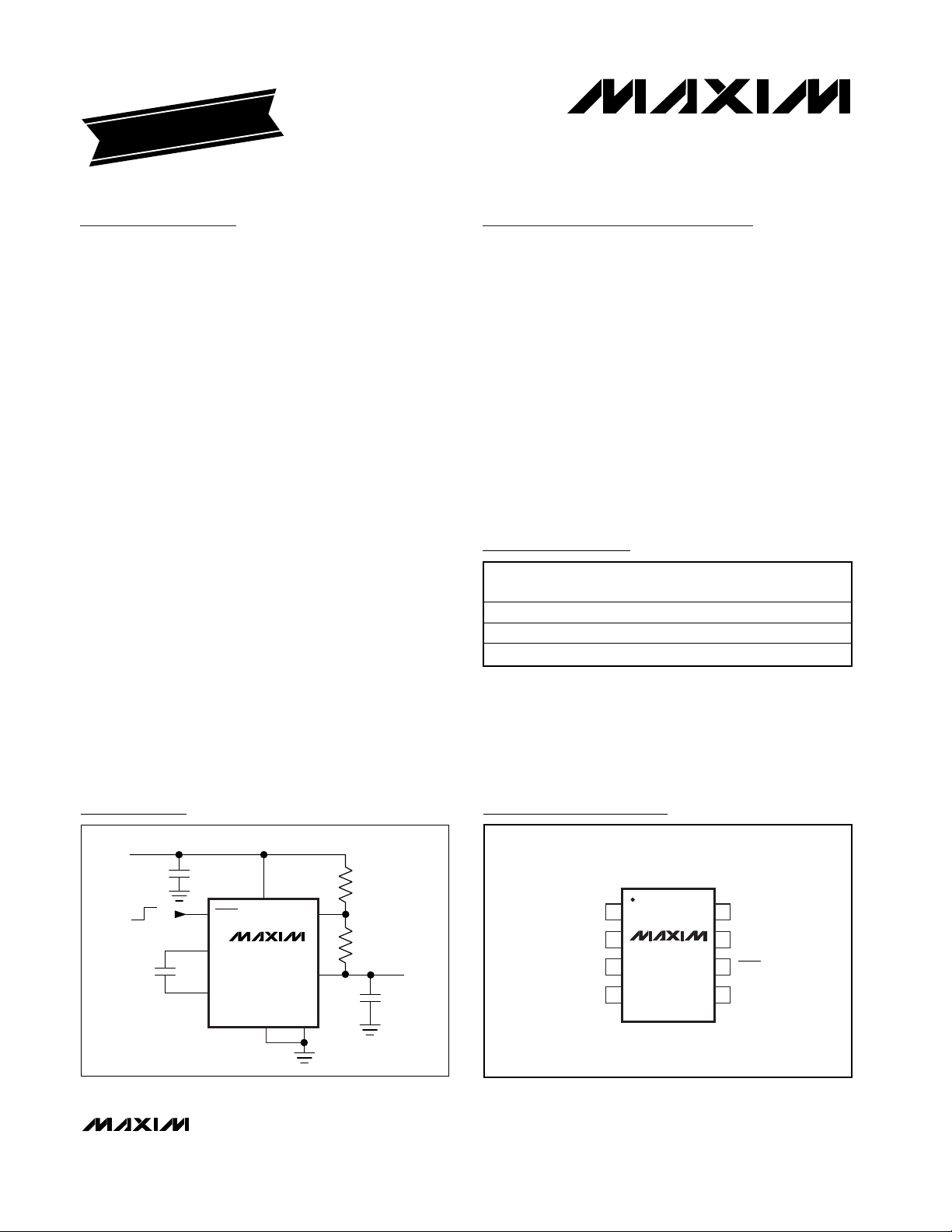
Pin Configuration
MAX889
IN
INPUT +2.7V TO +5.5V
REGULATED
NEGATIVE
OUTPUT
(UP TO -1 × V
IN
,
UP TO 200mA)
FB
OUT
GNDAGND
CAP+
ON
OFF
SHDN
CAP-
Typical Operating Circuit
19-1774; Rev 0; 7/00
For free samples and the latest literature, visit www.maxim-ic.com or phone 1-800-998-8800.
For small orders, phone 1-800-835-8769.
Ordering Information
PART
TEMP.
RANGE
PIN-
SWITCHING
FREQUENCY
8 SO 2MHz
8 SO 1MHz
8 SO 0.5MHz
EVALUATION KIT
AVAILABLE
PACKAGE
MAX889TESA -40°C to +85°C
MAX889SESA -40°C to +85°C
MAX889RESA -40°C to +85°C
TOP VIEW
IN
1
2
GND
3
4
87AGND
MAX889
SO
FBCAP+
SHDN
6
OUTCAP-
5
Page 2
MAX889
High-Frequency, Regulated,
200mA, Inverting Charge Pump
2 _______________________________________________________________________________________
ABSOLUTE MAXIMUM RATINGS
ELECTRICAL CHARACTERISTICS
(VIN= V
SHDN
= +5V, capacitors from Table 1, TA= 0°C to +85°C, unless otherwise noted. Typical values are at TA= +25°C.)
Stresses beyond those listed under “Absolute Maximum Ratings” may cause permanent damage to the device. These are stress ratings only, and functional
operation of the device at these or any other conditions beyond those indicated in the operational sections of the specifications is not implied. Exposure to
absolute maximum rating conditions for extended periods may affect device reliability.
IN to GND .................................................................-0.3V to +6V
FB, SHDN, CAP+ to GND............................-0.3V to (V
IN
+ 0.3V)
AGND to GND .......................................................-0.3V to +0.3V
OUT to GND .............................................................-6V to +0.3V
CAP- to GND ............................................(V
OUT
- 0.3V) to +0.3V
Continuous Output Current ...............................................250mA
Output Short-Circuit Duration ........................................Indefinite
Continuous Power Dissipation (T
A
= +70°C)
8-Pin SO (derate 5.88mW/°C above +70°C)...............471mW
Operating Temperature Range...........................-40°C to +85°C
Junction Temperature......................................................+150°C
Storage Temperature Range .............................-65°C to +150°C
Lead Temperature (soldering, 10s) ................................+300°C
PARAMETER
CONDITIONS
Supply Voltage Range V
IN
R
LOAD
= 100Ω 2.7
V
Output Voltage Range V
OUT
R
LOAD
= 100Ω
V
VIN = 5V, V
OUT
= -3.3V
Maximum Output Current
VIN = 3.3V, V
OUT
= -2.5V
mA
MAX889R 6 12
MAX889S 12 24
Quiescent Supply
Current (Free-Run Mode)
)
No load, VFB = V
IN
MAX889T 24 48
mA
MAX889R 3.3 7
MAX889S 5.5 12
Quiescent Supply
Current (Regulated Mode)
)
-3.3V
MAX889T 11 22
mA
Shutdown Supply Current I
SHDN
V
SHDN
= 0 0.1 50 µA
Open-Loop Output
Resistance (Free-Run Mode)
R
O
VFB = V
IN
2.0
Ω
Output Resistance
R
O(REG1)
V
OUT
regulated to -3.3V
Ω
SHDN, FB Input Bias Current ±1 µA
FB Input Offset Voltage I
LOAD
= 0 ±3
mV
Load Regulation I
OUT
= 0 to 200mA 10 mV
IN Undervoltage Lockout
Threshold
V
IN
rising (30mV hysteresis) 2.3
V
SHDN Logic High V
IH
SHDN Logic Low V
IL
VIN = +2.7V to +5.5V
V
MAX889R
0.5
0.62
MAX889S
1
Switching Frequency f
OSC
MAX889T 1.5 2
Thermal Shutdown Threshold
Junction temperature rising
(15°C hysteresis)
160 °C
SYMBOL
MIN TYP MAX UNITS
-2.5 -V
I
OUT(MAX)1
I
OUT(MAX)2
I
Q(FREE-RUN
200
145
5.5
IN
I
Q(REGULATED
No load, V
regulated to
OUT
0.7 x V
0.375
0.75
0.05
IN
0.3 x V
4.5
±35
2.6
1.25
2.5
IN
MHz
Page 3
MAX889
High-Frequency, Regulated,
200mA, Inverting Charge Pump
_______________________________________________________________________________________ 3
Note 1: Specifications to -40°C are guaranteed by design, not production tested.
ELECTRICAL CHARACTERISTICS
(VIN= V
SHDN
= +5V, capacitors from Table 1, TA= -40°C to +85°C, unless otherwise noted.) (Note 1)
PARAMETER
CONDITIONS
UNITS
Supply Voltage Range V
IN
R
LOAD
= 100Ω 2.7
V
Output Voltage Range V
OUT
R
LOAD
= 100Ω
V
VIN = 5V, V
OUT
= -3.3V
Maximum Output Current
VIN = 3.3V, V
OUT
= -2.5V
mA
MAX889R 12
MAX889S 24
Quiescent Supply
Current (Free-Run Mode)
)
No load, VFB = V
IN
MAX889T 48
mA
MAX889R 7
MAX889S 12
Quiescent Supply
Current (Regulated Mode)
)
-3.3V
MAX889T 22
mA
Shutdown Supply Current I
SHDN
V
SHDN
= 0 50 µA
Open-Loop Output
Resistance (Free-Run Mode)
R
O
VFB = V
IN
Ω
SHDN FB Input Bias Current ±1 µA
FB Input Offset Voltage I
LOAD
= 0
mV
IN Undervoltage Lockout
Threshold
V
IN
rising (30mV hysteresis) 2.3
V
SHDN Logic High V
IH
SHDN Logic Low V
IL
VIN = +2.7V to +5.5V
V
MAX889R
0.62
MAX889S
Switching Frequency f
OSC
MAX889T 1.5
MHz
Typical Operating Characteristics
(Circuit of Figure 1, VIN= V
SHDN
= +5V, capacitors from Table 1, TA= +25°C, unless otherwise noted.)
OUTPUT VOLTAGE
vs. LOAD CURRENT
MAX889 toc01
OUTPUT LOAD CURRENT (mA)
OUTPUT VOLTAGE (V)
-3.33
-3.32
-3.31
-3.30
-3.29
-3.28
-3.27
-3.26
-3.25
0 200 400 600 800
MAX889T
MAX889S
MAX889R
0
10
20
30
40
MAX889R
OUTPUT RIPPLE
vs. LOAD CURRENT vs. C
OUT
MAX889 toc02
LOAD CURRENT (mA)
OUTPUT RIPPLE (mV)
0 150 20050 100 250 300 350
C
OUT
= 22µF
C
OUT
= 47µF
C
OUT
= 10µF
0
10
20
30
40
MAX889S
OUTPUT RIPPLE
vs. LOAD CURRENT vs. C
OUT
MAX889 toc03
LOAD CURRENT (mA)
OUTPUT RIPPLE (mV)
0 150 20050 100 250 300 350
C
OUT
= 4.7µF
C
OUT
= 22µF
C
OUT
= 10µF
SYMBOL
I
OUT(MAX)1
I
OUT(MAX)2
I
Q(FREE-RUN
I
Q(REGULATED
No load, V
regulated to
OUT
MIN MAX
-2.5 -V
200
145
0.7 x V
IN
0.3 x V
0.375
0.75 1.25
5.5
IN
4.5
±35
2.6
IN
2.5
Page 4

MAX889
High-Frequency, Regulated,
200mA, Inverting Charge Pump
4 _______________________________________________________________________________________
Typical Operating Characteristics (continued)
(Circuit of Figure 1, VIN= V
SHDN
= +5V, capacitors from Table 1, TA= +25°C, unless otherwise noted.)
MAX889S
LOAD-TRANSIENT RESPONSE
MAX889 toc10
40µs/div
A
B
20 TO 200mA LOAD STEP
CIRCUIT OF FIGURE 4
A: I
OUT
, 100mA/div
B: V
OUT
, 20mV/div, AC-COUPLED
MAX889S
LINE-TRANSIENT RESPONSE
MAX889 toc11
40µs/div
A
B
I
OUT
= 200mA
CIRCUIT OF FIGURE 4
A: V
IN
, 2V/div
B: V
OUT
, 10mV/div, AC-COUPLED
MAX889S
STARTUP AND SHUTDOWN
MAX889 toc12
2ms/div
A
B
I
OUT
= 200mA
A: V
OUT
, 1V/div
B: I
IN
, 100mA/div
C: V
SHDN
, 10V/div
C
0
0
1.50
2.00
1.75
2.50
2.25
2.75
3.00
2.5 3.5 4.03.0 4.5 5.0 5.5
FREE-RUN OUTPUT RESISTANCE
vs. INPUT VOLTAGE
MAX889 toc07
INPUT VOLTAGE (V)
R
OUT
(Ω)
1.0
1.5
2.0
2.5
3.0
FREE-RUN OUTPUT RESISTANCE
vs. TEMPERATURE
MAX889 toc08
TEMPERATURE (°C)
R
OUT
(Ω)
-40 20 40-20 0 60 80
0
4
2
8
6
10
12
2.5 3.5 4.03.0 4.5 5.0 5.5
QUIESCENT SUPPLY CURRENT
vs. INPUT VOLTAGE (REGULATED MODE)
MAX889 toc09
INPUT VOLTAGE (V)
QUIESCENT CURRENT (mA)
MAX889T
MAX889S
MAX889R
V
OUT
= -2.5V
vs. LOAD CURRENT vs. C
50
40
30
20
OUTPUT RIPPLE (mV)
10
0
0 10050 150 200 250 300 350
MAX889T
OUTPUT RIPPLE
C
= 2.2µF
OUT
C
LOAD CURRENT (mA)
EFFICIENCY vs. LOAD CURRENT
OUT
C
= 4.7µF
OUT
= 10µF
OUT
MAX889 toc04
= 5V, V
(V
100
90
80
70
60
50
40
EFFICIENCY (%)
30
20
10
0
0200100 300 400 500
IN
MAX889R
MAX889T
MAX889S
LOAD CURRENT (mA)
OUT
= -3.3V)
MAX889 toc05
EFFICIENCY vs. LOAD CURRENT
= 3.3V, V
(V
100
90
80
70
60
50
40
EFFICENCY (%)
30
20
10
0
IN
MAX889R
MAX889T
MAX889S
0 50 100 150 200 250 300 350
LOAD CURRENT (mA)
OUT
= -2.5V)
MAX889 toc06
Page 5

MAX889
High-Frequency, Regulated,
200mA, Inverting Charge Pump
_______________________________________________________________________________________ 5
Pin Description
PIN NAME FUNCTION
1 IN Power-Supply Positive Voltage Input
2 CAP+ Positive Terminal of Flying Capacitor
3 GND Power Ground
4 CAP- Negative Terminal of Flying Capacitor
5 OUT Inverting Charge-Pump Output
6 SHDN
Shutdown Control Input. Drive SHDN low to shut down the MAX889. Connect SHDN to IN for
normal operation.
7FB
Feedback Input. Connect FB to a resistor-divider from IN (or other positive reference voltage
source) to OUT for regulated output voltages. Connect to IN for free-run mode.
8 AGND Analog Ground
Detailed Description
The MAX889 high-current regulated charge-pump DCDC inverter provides up to 200mA. It features the highest available output current while using small
capacitors (Table 1). The three versions available differ
in their switching frequencies (f
OSC
)—MAX889R/
MAX889S/MAX889T with f
OSC
= 500kHz/1MHz/2MHz,
respectively. Higher frequencies allow the use of smaller components (Table 1). Even smaller capacitor values
than those listed in Table 1 are suitable when the
devices are loaded at less than their rated output current. Designed specifically for compact applications, a
complete regulating circuit requires only three small
capacitors and two resistors, Figure 1. In addition, the
MAX889 includes soft-start, shutdown control, short-circuit, and thermal protection.
The oscillator, control circuitry, and four power MOSFET
switches are included on-chip. The charge pump runs
continuously at the operating frequency. During one-half
of the oscillator period, switches S1 and S2 close
(Figure 2), charging the transfer capacitor (C
FLY
) to the
input voltage (CAP- = GND, CAP+ = IN). During the
other half cycle, switches S3 and S4 close (Figure 3),
transferring the charge on C
FLY
to the output capacitor
(CAP+ = GND, CAP- = OUT).
Voltage Regulation
Voltage regulation is achieved by controlling the flyingcapacitor charging rate. The MAX889 controls the
charge on C
FLY
by modulating the gate drive to S1
(Figure 2) to supply the charge necessary to maintain
output regulation. When the output voltage droops,
C
FLY
charges higher due to increased gate drive. Since
the device switches continuously, the regulation
scheme minimizes output ripple, and the output noise
spectrum contains well-defined frequency components.
Feedback voltage is sensed with a resistor-divider
between an externally supplied positive reference or
the supply voltage and the negative inverted output.
The feedback loop servos FB to GND. The effective
output impedance in regulation is 0.05Ω. The output
remains in regulation until dropout is reached. Dropout
depends on the output voltage setting and load current
(see Output Voltage vs. Load Current in Typical
Operating Characteristics).
Free-Run Mode
(Unregulated Voltage Inverter)
The MAX889 may be used in an unregulated voltage
inverter mode that does not require external feedback
resistors, minimizing board space. Connecting FB to IN
places the MAX889 in free-run mode. In this mode, the
charge pump operates to invert directly the input supply voltage (V
OUT
= -(VIN- I
OUT
x RO)). Output resis-
tance is typically 2Ω and can be approximated by the
following equation:
RO≅ [1 / (f
OSC
x C
FLY
) ] + 2RSW+
4ESR
CFLY
+ ESR
COUT
The first term is the effective resistance of an ideal
switched-capacitor circuit (Figures 2 and 3), and R
SW
is the sum of the charge pump’s internal switch resistances (typically 0.8Ω at VIN= 5V). The last two terms
take into consideration the equivalent series resistance
Page 6

MAX889
(ESR) of the flying and output capacitors. The typical
output impedance is more accurately determined from
the Typical Operating Characteristics.
Current Limit and Soft-Start
The MAX889 features a foldback current-limit/soft-start
scheme that allows it to limit inrush currents during
startup, overload, and output short-circuit conditions.
Additionally, it permits a safe, timed recovery from fault
conditions. This protects the MAX889 and prevents
low-current or higher output impedance input supplies
(such as alkaline cells) from being overloaded at startup or short-circuit conditions.
The MAX889 features two current-limit/soft-start levels
with corresponding response to rising and falling output voltage thresholds of -0.6V and -1.5V. When the
falling output voltage crosses -1.5V, such as during an
overload condition, the input current is immediately limited to 400mA by weakening the charge-pump switches. When the falling output voltage crosses -0.6V, such
as during a short-circuit condition, the MAX889 further
weakens the charge-pump switches, immediately limiting input current to 200mA.
During startup or short-circuit recovery, the MAX889
limits input current to 200mA with charge-pump switches at their weakest level. Rising output voltage crossing
-0.6V initiates a 2ms timer, after which the MAX889
increases switch strength to the next level. The rising
output voltage crossing -1.5V initiates a 2ms timer, after
which the MAX889 provides full-strength operation.
Shutdown
When SHDN (a CMOS-compatible input) is driven low,
the MAX889 enters 0.1µA shutdown mode. Charge-
pump switching halts. Connect SHDN to IN or drive
high for normal operation.
Thermal Shutdown
The MAX889 features thermal shutdown with hysteresis
for added protection against fault conditions. When the
die temperature exceeds 160°C, the internal oscillator
stops, suspending device operation. The MAX889
resumes operation when the die temperature falls 15°C.
This prevents the device from rapidly oscillating around
the temperature trip point.
Applications Information
Resistor Selection
(Setting the Output Voltage)
The accuracy of V
OUT
depends on the accuracy of the
voltage biasing R1 in Figure 1. Use a separate reference voltage if greater accuracy than provided by V
IN
is desired (Figure 4). Keep the feedback node as small
as possible, with resistors mounted close to the FB pin.
High-Frequency, Regulated,
200mA, Inverting Charge Pump
6 _______________________________________________________________________________________
Figure 1. Typical Application Circuit.
Figure 3. Transferring Charge on C
FLY
to C
OUT
Figure 2. Charging C
FLY
S1
IN
S2
F
OSC
S3
CAP+
C
FLY
CAP-
C
OUT
S4
OUT
INPUT
5.0V
C
IN
4.7µF
ON
6
OFF
C
FLY
1µF
SHDN
2
CAP+
4
CAP-
1
IN
MAX889T
8
FB
OUT
GND
3
R1
100k
7
R1
66.5k
5
C
OUT
4.7µF
OUTPUT
-3.3V
IN
F
OSC
S1
S2
CAP+
C
FLY
CAP-
S3
S4
C
OUT
OUT
Page 7

MAX889
High-Frequency, Regulated,
200mA, Inverting Charge Pump
_______________________________________________________________________________________ 7
Adjust the output voltage to a negative voltage from
-2.5V to -VINwith external resistors R1 and R2 as
shown in Figures 1 and 4. FB servos to GND. Choose
R1 to be 100kΩ or less. Calculate R2 for the desired
output voltage:
V
OUT
= -V
REF
(R2 / R1)
R2 = R1 (V
OUT
/ -V
REF
)
where V
REF
can be either VINor a positive reference
source.
Typically, choose a voltage-divider current of at least
30µA to minimize the effect of FB input current and
capacitance:
R1 ≤ V
REF
/ 30µA
R2 < -V
OUT
/ 30µA
Capacitor Selection
The appropriate capacitors used with the MAX889
depend on the switching frequency. Table 1 provides
suggested values for CIN, C
FLY
, and C
OUT
.
Surface-mount ceramic capacitors are preferred for
CIN, C
OUT
, and C
FLY
due to their small size, low cost,
and low ESR. To ensure proper operation over the
entire temperature range, choose ceramic capacitors
with X7R (or equivalent) low-temperature-coefficient
(tempco) dielectrics. See Table 2 for a list of suggested
capacitor suppliers.
The output capacitor stores the charge transferred from
the flying capacitor and services the load between
oscillator cycles. A good general rule is to make the
output capacitance at least five-times greater than the
flying capacitor.
Output voltage ripple is largely dependent on C
OUT
.
Choosing a low-ESR capacitor of sufficient value is important in minimizing the peak-to-peak output voltage ripple,
which is approximated by the following equation:
where C
OUT
is the output capacitor value, ESR
COUT
is
the output capacitor’s ESR, and f
OSC
is the MAX889
switching frequency. Ceramic capacitors have the lowest
ESR and are recommended for C
OUT
. Where larger
capacitance at low cost is desired, a low-ESR tantalum
capacitor may be used for C
OUT
. See Table 2 for a list of
suggested capacitor suppliers.
To ensure stability over the entire operating temperature
range, choose a low-ESR output capacitor using the following equation:
where C
OUT
is the output capacitor value, and f
MIN
is the
minimum oscillator frequency in the Electrical
Characteristics table.
To ensure stability for regulated output mode, suitable
output capacitor ESR should be determined by the following equation:
Power Dissipation
The power dissipated in the MAX889 depends on the
input voltage, output voltage, and output current. Device
power dissipation is accurately described by:
P
DISS
= I
OUT(VIN
- (-V
OUT
)) + (I
Q
✕
VIN)
where IQis the device quiescent current. P
DISS
must be
less than the package dissipation rating (see Absolute
Maximum Ratings). Pay particular attention to power dissipation limits when generating small negative voltages
from large positive input voltages.
Layout Considerations
The MAX889’s high oscillator frequencies demand
good layout techniques that ensure stability and help
maintain the output voltage under heavy loads. Take
the following steps to ensure optimum layout:
1) Mount all components as close together as possible.
2) Place the feedback resistors R1 and R2 close to the
FB pin, and minimize the PC trace length at the FB
circuit node.
3) Keep traces short to minimize parasitic inductance
and capacitance.
4) Use a ground plane with CINand C
OUT
placed in a
star ground configuration (see the MAX889SEVKIT
layout).
V =
RIPPLE
2 x I ESR
OUT COUT
I
OUT
2 x f C
OSC OUT
+
C
OUT
15.5
≥
f
MIN
R1 + R2
R1
I
OUT
I
OUT
-3
1
R2
+
R1
R
≤
ESR
19.2 x 10
Page 8

MAX889
High-Frequency, Regulated,
200mA, Inverting Charge Pump
Maxim cannot assume responsibility for use of any circuitry other than circuitry entirely embodied in a Maxim product. No circuit patent licenses are
implied. Maxim reserves the right to change the circuitry and specifications without notice at any time.
8 _____________________Maxim Integrated Products, 120 San Gabriel Drive, Sunnyvale, CA 94086 408-737-7600
© 2000 Maxim Integrated Products Printed USA is a registered trademark of Maxim Integrated Products.
Table 1. Capacitor Selection Table
Table 2. Low-ESR Capacitor Manufacturers
Chip Information
TRANSISTOR COUNT: 1840
PROCESS: BiCMOS
Package Information
Figure 4. Separate VREF for Voltage Divider
PART FREQUENCY C
FLY
C
OUT
C
IN
REGULATED
MAX889R 0.5MHz 4.7µF22µF22µF 4.7µF
MAX889S 1MHz 2.2µF10µF10µF 2.2µF
MAX889T 2MHz 1µF 4.7µF 4.7µF1µF
PRODUCTION
METHOD
Surface-Mount
Tantalum
S ur face- M ount P ol ym er Sanyo POSCAP-APA 619-661-6835 619-661-1055
S ur face- M ount C er am i c
MANUFACTURER SERIES PHONE FAX
AVX TPS series 803-946-0690 803-626-3123
Kemet 494 series 864-963-6300 864-963-6521
Matsuo 267 series 714-969-2491 714-960-6492
Sprague 593D, 595D series 603-224-1961 603-224-1430
AVX X7R 803-946-0690 803-626-3123
Kemet X7R 864-963-6300 864-963-6521
Matsuo X7R 714-969-2491 714-960-6492
Murata GRM X7R 814-237-1431 814-238-0490
C
IN
FREE-RUN
SOICN.EPS
V
REF
OUT
5V
R1
100k
7
FB
R2
66.5k
5
4.7µF
3
C
OUT
V
OUT
R1
OUTPUT
-3.3V
= -V
REF
R2
×
INPUT
5.0V
OFF
C
1µF
C
4.7µF
FLY
IN
ON
6
SHDN
2
CAP+
4
CAP-
1
IN
MAX889T
GNDAGND
8
 Loading...