

Page 1
General Description
The MAX8884Y/MAX8884Z step-down converters with
dual low-dropout (LDO) linear regulators are intended to
power low-voltage microprocessors, DSPs, camera and
Wi-Fi modules, or other point of load applications in
portable devices. These ICs feature high efficiency with
small external component size. The step-down converter
output voltage is pin selectable between 1.2V and 1.8V,
and provides guaranteed output current of 700mA. The
2/4MHz hysteretic-PWM control scheme allows for tiny
external components and reduces no-load operating
current to 50μA. Two low quiescent current, low-noise
LDOs operate down to 2.7V supply voltage. Two switching frequency options are available—MAX8884Y (2MHz)
and MAX8884Z (4MHz)—allowing optimization for smallest solution size or highest efficiency. Fast switching
allows the use of small ceramic 2.2μF input and output
capacitors while maintaining low ripple voltage. The
MAX8884Y/MAX8884Z have individual enables for each
output, maximizing flexibility.
The MAX8884Y/MAX8884Z are available in a 16-bump,
2mm x 2mm CSP package (0.7mm max height).
Applications
Cell Phones/Smartphones
PDA and Palmtop Computers
Portable MP3 and DVD Players
Digital Cameras, Camcorders
PCMCIA Cards
Handheld Instruments
Features
♦ Step-Down Converter
Pin-Selectable Output Voltage (1.2V/1.8V)
2MHz or 4MHz Switching Frequency
Low-Output Voltage Ripple
700mA Output Drive Capability
Simple Logic ON/OFF Control
Tiny External Components
♦ Low-Noise LDOs
2 x 300mA LDO
Pin-Selectable Output Voltage (LDO1)
Low 26µV
RMS
(typ) Output Noise
High 65dB (typ) PSRR
Simple Logic ON/OFF Control
♦ Low 0.1µA Shutdown Current
♦ 2.7V to 5.5V Supply Voltage Range
♦ Thermal Shutdown
♦ Tiny, 2mm x 2mm x 0.65mm CSP Package (4x4 Grid)
MAX8884Y/MAX8884Z
700mA DC-DC Step-Down Converters
with Dual 300mA LDO in 2mm x 2mm CSP
________________________________________________________________
Maxim Integrated Products
1
19-4418; Rev 0; 4/09
For pricing, delivery, and ordering information, please contact Maxim Direct at 1-888-629-4642,
or visit Maxim’s website at www.maxim-ic.com.
Typical Application Circuit appears at end of data sheet.
AGND
PGND
REFBP
NC1
BUCK_EN
LX
LDO2
LDO2_EN
MAX8884Y
MAX8884Z
SEL
IN1A
IN2
IN1B
LDO1_EN
FB
LDO1
NC2
TOP VIEW
(BUMPS ON BOTTOM)
A1 A2 A3 A4
B1 B2 B3 B4
C1 C2 C3 C4
D1 D2 D3 D4
CSP
Pin Configuration
IN1A
LX
FB
2.2μH
AGND
BUCK_EN
LDO1_EN
LDO2_EN
IN2
BATT
2.7V TO 5.5V
BATT
2.7V TO 5.5V
BUCK ON/OFF
BUCK
1.2V/1.8V
REFBP
IN1B
LDO1 ON/OFF
LDO2 ON/OFF
LDO2
LDO1
V
LDO2
UP TO 300mA
V
LDO1
UP TO 300mA
PGND
SEL
2.2μF
2.2μF
BUCK/LDO1 VOLTAGE
SELECTION
MAX8884Y
MAX8884Z
Typical Operating Circuit
Ordering Information
Note: All devices are specified over the -40°C to +85°C operating temperature range.
+
Denotes a lead(Pb)-free/RoHS-compliant package.
T = Tape and reel.
PART PIN-PACKAGE
MAX8884YEREKE+T 16 CSP 2MHz
MAX8884ZEREKE+T 16 CSP 4MHz
SWITCHING
FREQUENCY
Page 2
MAX8884Y/MAX8884Z
700mA DC-DC Step-Down Converters
with Dual 300mA LDO in 2mm x 2mm CSP
2 _______________________________________________________________________________________
ABSOLUTE MAXIMUM RATINGS
ELECTRICAL CHARACTERISTICS
(V
IN1A
= V
IN1B
= V
IN2
= V
LDO1_EN
= V
LDO2_EN
= V
BUCK_EN
= 3.6V. TA= -40°C to +85°C, typical values are at TA= +25°C, unless
otherwise noted.) (Note 1)
Stresses beyond those listed under “Absolute Maximum Ratings” may cause permanent damage to the device. These are stress ratings only, and functional
operation of the device at these or any other conditions beyond those indicated in the operational sections of the specifications is not implied. Exposure to
absolute maximum rating conditions for extended periods may affect device reliability.
IN1A, IN1B, IN2, REFBP to AGND ........................-0.3V to +6.0V
FB to PGND ...........................................................-0.3V to +6.0V
SEL, BUCK_EN to AGND...............-0.3V to (V
IN1A
/V
IN1B
+ 0.3V)
LDO1, LDO2, LDO1_EN, LDO2_EN
to AGND.................................................-0.3V to (V
IN2
+ 0.3V)
IN2 to IN1A, IN1B ..................................................-0.3V to +0.3V
AGND to PGND .....................................................-0.3V to +0.3V
IN1A, IN1B, LX Current .....................................................1A
RMS
Continuous Power Dissipation (TA= +70°C)
16-Bump CSP (derate 12.5mW/°C above +70°C) ..............1W
Operating Temperature .......................................-40°C to +85°C
Junction Temperature......................................................+150°C
Storage Temperature Range .............................-65°C to +150°C
Bump Temperature*.........................................................+260°C
*
These ICs are constructed using a unique set of packaging techniques imposing a limit on the thermal profile used during board level
solder attach and rework. This limit permits only the use of the solder profiles recommended in the industry-standard specification,
JEDEC 020A, paragraph 7.6, Table 3 for IR/VPR and Convection reflow. Preheating is required. Hand or wave soldering is not allowed.
INPUT SUPPLY
Input Voltage V
Input Undervoltage Threshold V
Shutdown Supply Current
No-Load Supply Current
THERMAL PROTECTION
Thermal Shutdown TA rising, 20°C typical hysteresis +160 °C
LOGIC CONTROL
Logic Input-High Voltage
(BUCK_EN, SEL, LDO1_EN,
LDO2_EN)
PARAMETER CONDITIONS MIN TYP MAX UNITS
, V
, V
IN1A
, V
IN1A
V
BUCK_ EN
V
LDO2_EN
V
BUCK_ EN
V
LDO1_EN
2.7V V
IN1B
IN1B
IN1A
2.7 5.5 V
IN2
, V
rising, 180mV typical hysteres is 2.52 2.63 2.70 V
IN2
= V
LDO1_EN
=
= 0
= 0, I
= V
= V
LDO1
LDO2_EN
IN1B
= I
= 0, I
= V
TA= +25°C 0.1 4
T
= +85°C 0.1
A
= 0A 140 230 μA
LDO2
= 0A, no switching 50 80 μA
BUCK
5.5V 1.3 V
IN2
μA
Logic Input-Low Voltage
(BUCK_EN, SEL, LDO1_EN,
2.7V V
IN1A
= V
IN1B
= V
5.5V 0.4 V
IN2
LDO2_EN)
Logic Input Current (BUCK_EN,
SEL, LDO1_EN, LDO2_EN)
V
= 0 or VIH= V
IL
IN1A
= 5.5V
TA = +25°C 0.01 1
= +85°C 0.1
T
A
FB
Buc k Con verter Output Voltage
FB Leakage Current
SEL = AGND, I
= V
V
SEL
IN1A
V
= V
V
IN1A
FB
IN1B
= 0
= 0A 1.18 1.22 1.24 V
BUCK
, I
= 0A 1.78 1.80 1.85 V
BUCK
= V
= 5.5V,
IN2
TA = +25°C 0.01 1
T
= +85°C 1
A
LX
On-Resistance
p-channel MOSFET switch, ILX = -40mA 0.18 0.30
n-channel MOSFET rectifier, I
= 40mA 0.15 0.25
LX
μA
μA
Page 3
MAX8884Y/MAX8884Z
700mA DC-DC Step-Down Converters
with Dual 300mA LDO in 2mm x 2mm CSP
_______________________________________________________________________________________ 3
ELECTRICAL CHARACTERISTICS (continued)
(V
IN1A
= V
IN1B
= V
IN2
= V
LDO1_EN
= V
LDO2_EN
= V
BUCK_EN
= 3.6V. TA= -40°C to +85°C, typical values are at TA= +25°C, unless
otherwise noted.) (Note 1)
Note 1: All devices are 100% production tested at T
A
= +25°C. Limits over the operating temperature range are guaranteed by
design.
LX Leakage Current
p-Channel MOSFET Peak Current
Limit
n-Channel MOSFET Valley
Current Lim it
n-Channel MOSFET
Zero-Crossing Threshold
Min imum On-Time 0.07 μs
Minimum Off-Time 0.06 μs
Power-Up Delay From V
LDO1, LDO2
Output Voltage V
Output Voltage V
Output Current 300 mA
Current Lim it V
Dropout Voltage I
Line Regulation V
Load Regulation I
Power-Supply Rejection
V
LDO_
Output Noise
Output Capacitor for Stable
Operation
Shutdown Output Impedance V
Power-Up Delay From V
REFBP
REFBP Output Voltage 0 I
REFBP Supply Rejection V
PARAMETER CONDITIONS MIN TYP MAX UNITS
= V
V
IN1A
= 0
V
LX
= 0 0.8 1.0 1.2 A
V
LX
IN1B
= V
IN2
= 5.5V,
TA= +25°C 0.1 1
T
= +85°C 1
A
0.6 0.8 1.0 A
MAX8884Y_ 40
MAX8884Z_ 60
rising to VLX rising 120 250 μs
LDO_
LDO_
LDO_
LDO_
= 1mA;
= 100mA
= 1mA;
= 100mA
LDO_
= 30mA
LDO_
LDO_
= 30mA
LDO_
= 1.8V,
= 1.8V,
SEL = AGND 1.764 1.800 1.836
SEL = IN1_ 2.800
2.770 2.800 2.830 V
2.5V) 70 200 mV
LDO_
= 100mA 2.4 mV
LDO_
65 dB
26 μV
< 10mA 0.1
< 200mA 1
LDO_
< 300mA 2.2
LDO_
= V
LDO2_EN
= 0 100
rising to V
output ri sing 150 250 μs
LDO_
1μA 1.237 1.250 1.263 V
/V
IN2
LDO1
LDO2
BUCK_ EN
V
= 5.5V, I
IN2
V
= 3.4V, I
IN2
V
= 5.5V, I
IN2
V
= 3.4V, I
IN2
= 0 310 450 750 mA
LDO_
= 100mA, TA= +25°C (V
LDO_
stepped from 3.5V to 5.5V, I
IN2
stepped from 50μA to 200mA 25 mV
LDO_
10Hz to 100 kHz, V
= 2.2μF, I
C
LDO_
10Hz to 100 kHz, V
C
= 2.2μF, I
LDO_
0 < I
LDO_
10mA < I
200mA < I
LDO1_EN
LDO_ EN
REFBP
stepped from 2.55V to 5.5V 0.2 5 mV
IN2
μA
mA
V
RMS
μF
Page 4
MAX8884Y/MAX8884Z
700mA DC-DC Step-Down Converters
with Dual 300mA LDO in 2mm x 2mm CSP
4 _______________________________________________________________________________________
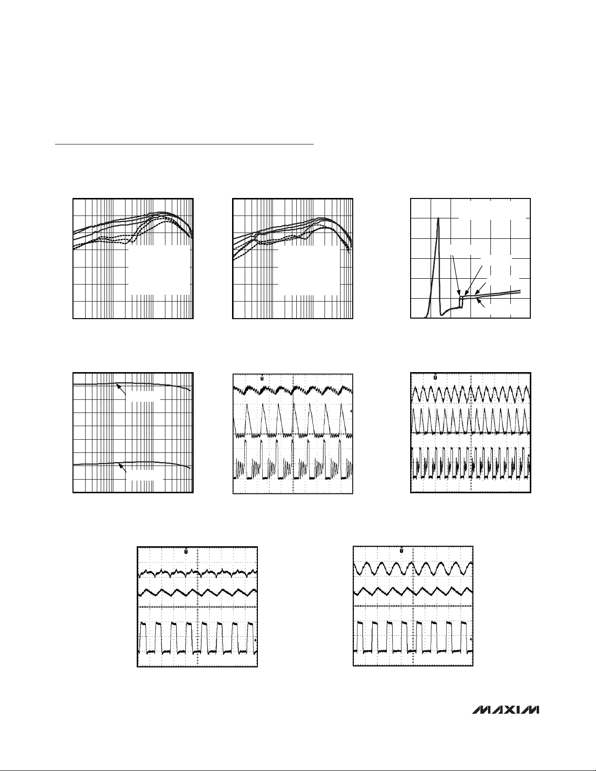
STEP-DOWN CONVERTER EFFICIENCY
vs. LOAD CURRENT, V
OUT
= 1.8V
MAX8884Y/Z toc01
LOAD CURRENT (mA)
EFFICIENCY (%)
10010
40
50
60
70
80
90
100
30
1 1000
MAX8884Y, VIN = 3.2V
= 3.6V
= 4.2V
MAX8884Z, V
IN
= 3.2V
= 3.6V
= 4.2V
STEP-DOWN CONVERTER EFFICIENCY
vs. LOAD CURRENT, V
OUT
= 1.2V
MAX8884Y/Z toc02
LOAD CURRENT (mA)
EFFICIENCY (%)
10010
40
50
60
70
80
90
100
30
1 1000
MAX8884Y, VIN = 3.2V
= 3.6V
= 4.2V
MAX8884Z, V
IN
= 3.2V
= 3.6V
= 4.2V
STEP-DOWN CONVERTER NO-LOAD
SUPPLY CURRENT vs. INPUT VOLTAGE
MAX8884Y/Z toc03
INPUT VOLTAGE (V)
SUPPLY CURRENT (μA)
54321
50
100
150
200
250
300
0
06
V
BUCK_EN
= V
IN
V
LDO1_EN
= V
LDO2_EN
= 0
VIN FALLING
VIN RISING
MAX8884Y
MAX8884Z
STEP-DOWN OUTPUT VOLTAGE vs. LOAD
CURRENT (VOLTAGE POSITIONING)
MAX8884Y/Z toc04
LOAD CURRENT (mA)
OUTPUT VOLTAGE (V)
10010
1.1
1.2
1.3
1.4
1.5
1.6
1.7
1.8
1.9
1.0
1 1000
SEL = IN1_
SEL = AGND
MAX8884Y STEP-DOWN CONVERTER
LIGHT LOAD SWITCHING WAVEFORMS
MAX8884Y/Z toc06
1μs/div
I
LX
V
OUT
V
LX
0A
2V/div
100mA/div
AC-COUPLED
10mV/div
0V
I
LOAD
= 50mA
MAX8884Z STEP-DOWN CONVERTER
HEAVY LOAD SWITCHING WAVEFORMS
MAX8884Y/Z toc07
200ns/div
I
LX
V
OUT
V
LX
0A
2V/div
500mA/div
AC-COUPLED
10mV/div
0V
I
LOAD
= 500mA
MAX8884Y STEP-DOWN CONVERTER
HEAVY LOAD SWITCHING WAVEFORMS
MAX8884Y/Z toc08
400ns/div
I
LX
V
OUT
V
LX
0A
2V/div
500mA/div
AC-COUPLED
10mV/div
0V
I
LOAD
= 500mA
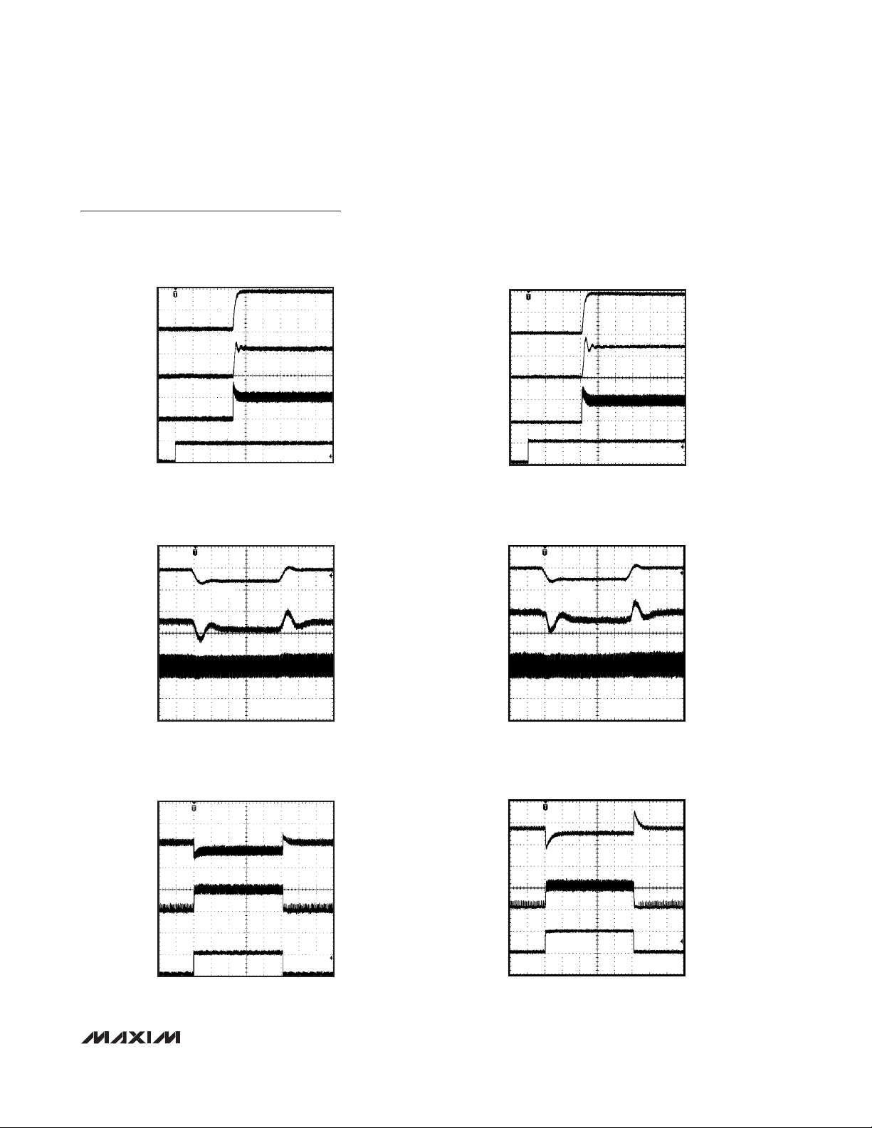
Typical Operating Characteristics
(VIN= V
IN1A
= V
IN1B
= V
IN2
= 3.6V, V
BUCK
= 1.2V, V
LDO1
= 1.8V, V
LDO2
= 2.8V, MAX8884YEVKIT, TA= +25°C, unless otherwise noted.)
MAX8884Z STEP-DOWN CONVERTER
LIGHT LOAD SWITCHING WAVEFORMS
MAX8884Y/Z toc05
V
OUT
V
AC-COUPLED
20mV/div
I
LX
LX
400ns/div
100mA/div
0A
2V/div
0V
Page 5
MAX8884Y/MAX8884Z
700mA DC-DC Step-Down Converters
with Dual 300mA LDO in 2mm x 2mm CSP
_______________________________________________________________________________________
5
MAX8884Z STEP-DOWN CONVERTER
LINE TRANSIENT RESPONSE
MAX8884Y/Z toc12
10μs/div
I
LX
V
IN
V
OUT
0A
1V/div
200mA/div
AC-COUPLED
20mV/div
I
LOAD
= 500mA
4V 4V
3.5V
MAX8884Y STEP-DOWN CONVERTER
LOAD TRANSIENT
MAX8884Y/Z toc14
20μs/div
I
LX
V
OUT
I
OUT
0A
1.8V DC OFFSET
100mV/div
500mA/div
500mA/div
0A
500mA
10mA 10mA
_______________________________________________________________________________________ 5
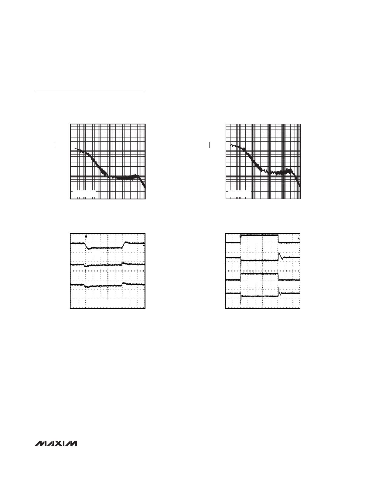
Typical Operating Characteristics (continued)
(VIN= V
IN1A
= V
IN1B
= V
IN2
= 3.6V, V
BUCK
= 1.2V, V
LDO1
= 1.8V, V
LDO2
= 2.8V, MAX8884YEVKIT, TA= +25°C, unless otherwise noted.)
MAX8884Z STEP-DOWN CONVERTER
LOAD TRANSIENT
MAX8884Y/Z toc13
20μs/div
V
OUT
I
LX
I
OUT
0A
500mA/div
0A
500mA/div
1.8V DC OFFSET
100mV/div
10mA10mA
500mA
MAX8884Z STEP-DOWN CONVERTER
SOFT-START WAVEFORMS
MAX8884Y/Z toc09
40μs/div
I
IN1
V
OUT
I
LX
V
BUCK_EN
0A
2V/div
500mA/div
0A
200mA/div
0V
1V/div
0V
I
LOAD
= 500mA
MAX8884Y STEP-DOWN CONVERTER
LINE TRANSIENT RESPONSE
4V 4V
V
IN
V
OUT
3.5V
MAX8884Y/Z toc11
1V/div
AC-COUPLED
20mV/div
MAX8884Y STEP-DOWN CONVERTER
V
BUCK_EN
SOFT-START WAVEFORMS
V
OUT
I
IN1
I
LX
40μs/div
I
LOAD
MAX8884Y/Z toc10
= 500mA
1V/div
0V
200mA/div
0A
500mA/div
0A
2V/div
0V
I
LX
I
= 500mA
LOAD
10μs/div
200mA/div
0A
Page 6

MAX8884Y/MAX8884Z
700mA DC-DC Step-Down Converters
with Dual 300mA LDO in 2mm x 2mm CSP
6 _______________________________________________________________________________________
Typical Operating Characteristics (continued)
(VIN= V
IN1A
= V
IN1B
= V
IN2
= 3.6V, V
BUCK
= 1.2V, V
LDO1
= 1.8V, V
LDO2
= 2.8V, MAX8884YEVKIT, TA= +25°C, unless otherwise noted.)
LDO POWER SUPPLY
RIPPLE REJECTION, V
OUT
= 1.8V
MAX8884Y/Z toc18
FREQUENCY (kHz)
RIPPLE REJECTION (dB)
100100.1 1
10
20
30
40
50
60
70
80
0
0.01 1000
I
LDO
= 30mA
LDO2 DROPOUT VOLTAGE
vs. LOAD CURRENT
MAX8884Y/Z toc17
LOAD CURRENT (mA)
DROPOUT VOLTAGE (V)
25020015010050
50
100
150
200
250
0
0 300
LDO POWER SUPPLY
RIPPLE REJECTION, V
OUT
= 2.8V
MAX8884Y/Z toc19
FREQUENCY (kHz)
RIPPLE REJECTION (dB)
1001010.1
10
20
30
40
50
60
70
0
0.01 1000
I
LDO_
= 30mA
LDO1, LDO2 INPUT SUPPLY CURRENT
vs. INPUT VOLTAGE
MAX8884Y/Z toc16
INPUT VOLTAGE (V)
SUPPLY CURRENT (μA)
54321
50
100
150
200
250
300
350
0
06
V
LDO1_EN
= V
LDO2_EN
= VIN,
V
BUCK_EN
= 0
MAX8884Y STEP-DOWN CONVERTER
SHUTDOWN WAVEFORMS
MAX8884Y/Z toc15
10μs/div
I
LX
V
OUT
V
BUCK_EN
0V
1V/div
0V
5V/div
500mA/div
0A
I
LOAD
= 500mA
LDO OUTPUT VOLTAGE
NOISE WAVEFORM, V
VN = 26.1μV
f = 100Hz to 100kHz, I
RMS
,
LDO_
400μs/div
OUT_
= 30mA
= 1.8V
MAX8884Y/Z toc20
MAX8884Y/MAX8884Z
LDO1 = 1.8 AT 30mA
= 3.6V
V
IN
50μV/div
Page 7
MAX8884Y/MAX8884Z
700mA DC-DC Step-Down Converters
with Dual 300mA LDO in 2mm x 2mm CSP
_______________________________________________________________________________________
7_______________________________________________________________________________________ 7
Typical Operating Characteristics (continued)
(VIN= V
IN1A
= V
IN1B
= V
IN2
= 3.6V, V
BUCK
= 1.2V, V
LDO1
= 1.8V, V
LDO2
= 2.8V, MAX8884YEVKIT, TA= +25°C, unless otherwise noted.)
LDO1, LDO2 LOAD TRANSIENT RESPONSE
MAX8884Y/Z toc24
20μs/div
I
LDO1
V
LDO2
I
LDO2
V
LDO1
AC-COUPLED
10mV/div
AC-COUPLED
10mV/div
50mA/div
50mA/div
1mA 1mA
1mA 1mA
40mA
40mA
LDO1, LDO2 LINE TRANSIENT
MAX8884Y/Z toc23
10μs/div
V
LDO1
V
IN
V
LDO2
AC-COUPLED
5mV/div
AC-COUPLED
5mV/div
1V/div
I
LDO1
= I
LDO2
= 100mA
4V 4V
3.5V
LDO OUTPUT-NOISE SPECTRAL DENSITY
vs. FREQUENCY, V
10,000
1000
100
NOISE DENSITY (nV√(Hz))
I
= 30mA
LDO_
10
0.01 1000
FREQUENCY (kHz)
LDO_
= 1.8V
1001010.1
MAX884Y/Z toc21
LDO OUTPUT-NOISE SPECTRAL DENSITY
vs. FREQUENCY, V
10,000
1000
100
NOISE DENSITY (nV√(Hz))
I
= 30mA
LDO_
10
0.01 1000
FREQUENCY (kHz)
LDO_
= 2.8V
1001010.1
MAX884Y/Z toc22
Page 8

MAX8884Y/MAX8884Z
700mA DC-DC Step-Down Converters
with Dual 300mA LDO in 2mm x 2mm CSP
8 _______________________________________________________________________________________
Typical Operating Characteristics (continued)
(VIN= V
IN1A
= V
IN1B
= V
IN2
= 3.6V, V
BUCK
= 1.2V, V
LDO1
= 1.8V, V
LDO2
= 2.8V, MAX8884YEVKIT, TA= +25°C, unless otherwise noted.)
LDO1, LDO2 LOAD TRANSIENT
RESPONSE NEAR DROPOUT
I
LDO2
1mA 1mA
V
LDO2
I
LDO1
1mA 1mA
V
LDO1
40mA
40mA
V
20μs/div
MAX8884Y/Z toc25
50mA/div
AC-COUPLED
10mV/div
50mA/div
AC-COUPLED
10mV/div
= V
+ 200mV
IN2
LDO2
REFBP SOFT-START
V
REFBP
V
LDO1_EN
V
LDO1
C
REFBP
= 0.033μF
MAX8884Y/Z toc27
1V/div
0V
2V/div
0V
1V/div
0V
V
LDO1_EN
V
LDO2_EN
V
LDO1_EN
V
V
LDO1
V
LDO2
REFBP
V
LDO1
LDO1, LDO2 STARTUP
AND SHUTDOWN RESPONSE
=
REFBP SOFT-START
C
REFBP
400μs/div
= 0.15μF
MAX8884Y/Z toc26
MAX8884Y/Z toc28
2V/div
0V
2V/div
0V
2V/div
0V
1V/div
0V
2V/div
0V
1V/div
0V
100μs/div
100μs/div
Page 9

MAX8884Y/MAX8884Z
700mA DC-DC Step-Down Converters
with Dual 300mA LDO in 2mm x 2mm CSP
_______________________________________________________________________________________ 9
Detailed Description
The MAX8884Y/MAX8884Z are designed to power the
subcircuits within a system. These ICs contain a highfrequency, high-efficiency step-down converter and two
LDOs. The step-down converter delivers 700mA with
either 1.2V or 1.8V selectable output voltage using SEL.
The hysteretic PWM control scheme provides extremely
fast transient response, while 2MHz and 4MHz switching frequency options allow the trade-off between efficiency and the smallest external components. The
MAX8884Y/MAX8884Z linear regulators can be used to
power loads requiring a low output noise supply.
Step-Down Converter Control Scheme
A hysteretic PWM control scheme ensures high efficiency, fast switching, fast transient response, low-output
voltage ripple, and physically tiny external components.
The control scheme is simple: when the output voltage
is below the regulation threshold, the error comparator
begins a switching cycle by turning on the high-side
switch. This high-side switch remains on until the minimum on-time expires and output voltage is within regulation, or the inductor current is above the current-limit
threshold. Once off, the high-side switch remains off
until the minimum off-time expires and the output voltage falls again below the regulation threshold. During
Pin Description
PIN NAME FUNCTION
A1 REFBP
A2 AGND Low-Noise Analog Ground. Connect to common ground plane.
A3 NC1 No Internal Connection. Connect NC1 to ground.
A4 PGND Power Ground for Step-Down Converter. Connect to common ground plane.
B1 LDO2
B2 BUCK_EN
B3 LDO2_EN
B4 LX Inductor Connection. Connect an inductor from LX to the output of the step-down converter.
C1 IN2
C2 SEL
C3, C4 IN1B, IN1A
D1 LDO1
D2 LDO1_EN
D3 NC2 No Internal Connection. Connect NC2 to ground.
D4 FB FB is Connected to the Internal Feedback Network
Reference Noise Bypass. Bypass REFBP to AGND with a 0.033μF ceramic capacitor to reduce noise
on the LDO outputs. REFBP is internally pulled to ground through a 1kΩ resistor during shutdown.
300mA LDO Regulator 2 Output. For 300mA application, bypass LDO2 with a 2.2μF ceramic capacitor
as close as possible to LDO2 and AGND. For low-output current capability, up to 10mA, an output
capacitor of 0.1μF is sufficient to keep the output voltage stable. LDO2 is internally pulled to ground
through a 100Ω resistor when this regulator is disabled.
Step-Down Converter Enable Input. Connect BUCK_EN to IN1_ or logic-high for normal operation.
Connect BUCK_EN to AGND or logic-low for step-down shutdown mode.
LDO2 Enable Input. Connect LDO2_EN to IN2 or logic-high for normal operation. Connect LDO2_EN to
AGND or logic-low for LDO2 shutdown mode.
Supply Voltage Input for LDO1, LDO2, and Internal Reference. Connect IN2 to a battery or supply
voltage from 2.7V to 5.5V. Bypass IN2 with a 4.7μF ceramic capacitor as close as possible to IN2 and
AGND. Connect IN2 to the same source as IN1A and IN1B.
Output Voltage Selection for LDO1 and Step-Down Converter. Connect to IN1_ or AGND for output
voltage selection. See Table 1.
Supply Voltage Input for Step-Down Converter. Connect IN1B and IN1A to a battery or supply voltage
from 2.7V to 5.5V. Bypass the connection of IN1B and IN1A with a 2.2μF ceramic capacitor as close as
possible to IN1B, IN1A, and PGND. IN1A
and IN1B to the same source as IN2.
300mA LDO Regulator 1 Output. For 300mA application, bypass LDO1 with a 2.2μF ceramic capacitor
as close as possible to LDO1 and AGND. For low-output current capability, up to 10mA, an output
capacitor of 0.1μF is sufficient to keep output voltage stable. LDO1 is internally pulled to AGND
through a 100Ω resistor when this regulator is disabled.
LDO1 Enable Input. Connect LDO1_EN to IN2 or logic-high for normal operation. Connect LDO1_EN to
AGND or logic-low for LDO1 shutdown mode.
and IN1B are internally connected together. Connect IN1A
Page 10

MAX8884Y/MAX8884Z
700mA DC-DC Step-Down Converters
with Dual 300mA LDO in 2mm x 2mm CSP
10 ______________________________________________________________________________________
the off period, the low-side synchronous rectifier turns
on and remains on until the high-side switch turns on
again. The internal synchronous rectifier eliminates the
need for an external Schottky diode.
At inductor currents below 40mA (60mA), the MAX8884Y
(MAX8884Z) automatically switches to pulse-skipping
mode to improve light-load efficiency. Output voltage
ripple remains low at all loads, while the skip-mode
switching frequency remains ultrasonic down to 1mA
(typ) loads.
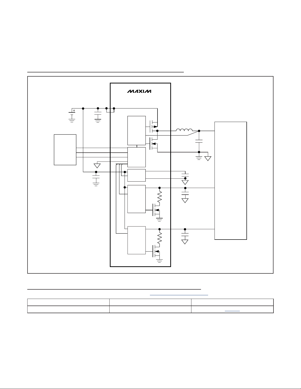
Voltage Positioning Load Regulation
The MAX8884Y/MAX8884Z step-down converters utilize
a unique feedback network. By taking a DC feedback
from the LX node through R1 in the
Block Diagram
, the
usual phase lag due to the output capacitor is
removed, making the loop exceedingly stable and
allowing the use of very small ceramic output capacitors. To improve the load regulation, resistor R3 is
included in the feedback (see the
Block Diagram
). This
configuration yields load regulation equal to half the
inductor’s series resistance multiplied by the load current. This voltage positioning load regulation greatly
reduces overshoot during load transients.
SEL Output Voltage Selection
SEL is used to determine the output voltage of the buck
converter and LDO1. See Table 1.
Shutdown Mode
Drive BUCK_EN to logic-low to place the MAX8884Y/
MAX8884Z step-down converter in shutdown mode. In
shutdown, the control circuitry, internal switching
MOSFET, and synchronous rectifier turn off and LX
becomes high impedance.
The LDOs are individually enabled. Connect LDO1_EN
and LDO2_EN to GND or logic-low to place LDO1 and
LDO2 in shutdown mode. In shutdown, the outputs of
the LDOs are pulled to ground through an internal
100Ω resistor.
When the step-down converter and all LDOs are in shutdown, the MAX8884Y/MAX8884Z enter a very low-power
state, where the input current drops to 0.1μA (typ).
Step-Down Converter Soft-Start
The MAX8884Y/MAX8884Z step-down converter uses
internal soft-start circuitry to limit inrush current at startup,
reducing transients on the input source. Soft-start is particularly useful for supplies with high output impedance such
as Li+ and alkaline cells. See the soft-start waveforms in
the
Typical Operating Characteristics
.
Thermal Shutdown
Thermal shutdown limits total power dissipation in the
MAX8884Y/MAX8884Z. If the junction temperature
exceeds +160°C, thermal shutdown circuitry turns off
the MAX8884Y/MAX8884Z, allowing the ICs to cool.
The ICs turn on and begin soft-start after the junction
temperature cools by 20°C. This results in a pulsed output during continuous thermal-overload conditions.
Applications Information
Output Voltages
The MAX8884Y/MAX8884Z DC-DC step-down converter sets the BUCK and LDO1 output voltage based on
the state of SEL. See Table 1.
Contact the factory for other output voltage options.
LDO Dropout Voltage
The regulator’s minimum input/output differential (or
dropout voltage) determines the lowest usable supply
voltage. In battery-powered systems, this determines the
useful end-of-life battery voltage. Because the
MAX8884Y/MAX8884Z LDOs use a p-channel MOSFET
pass transistor, their dropout voltages are a function of
drain-to-source on-resistance (R
DS(ON)
) multiplied by the
load current (see the
Typical Operating Characteristics
).
Inductor Selection
The MAX8884Y operates with a switching frequency of
2MHz and utilizes a 2.2μH inductor. The MAX8884Z
operates with a switching frequency of 4MHz and utilizes a 1μH inductor. The higher switching frequency of
the MAX8884Z allows the use of physically smaller
inductors at the cost of lower efficiency. The lower
switching frequency of the MAX8884Y results in greater
efficiency at the cost of a physically larger inductor.
See the
Typical Operating Characteristics
for efficiency
graphs for both the MAX8884Y and the MAX8884Z.
Table 1. SEL Output Voltage Selection
VV
I load cu
R DC impedance of inductor
V
=−
BUCK BUCK NO LOA D
=
LOAD
=
DCR
__AAD
BUCK NO LO
__
rrrent
V or V dependin g o n SEL=12 18..
IR
×
LOAD DCR
2
BUCK CONVERTER
SEL
AGND 1.2 1.8
IN1_ 1.8 2.8
OUTPUT VOLTAGE
(V)
LDO1
OUTPUT VOLTAGE
(V)
Page 11

MAX8884Y/MAX8884Z
700mA DC-DC Step-Down Converters
with Dual 300mA LDO in 2mm x 2mm CSP
______________________________________________________________________________________ 11
The inductor’s DC current rating only needs to match the
maximum load of the application because the
MAX8884Y/MAX8884Z feature zero current overshoot
during startup and load transients. For optimum transient
response and high efficiency, choose an inductor with
DC series resistance in the 50mΩ to 150mΩ range. See
Table 2 for suggested inductors and manufacturers.
Output Capacitor Selection
For the DC-DC step-down converter, the output capacitor
C
BUCK
is required to keep the output voltage ripple small
and ensure regulation loop stability. C
BUCK
must have low
impedance at the switching frequency. Ceramic capacitors with X5R or X7R dielectric are highly recommended
due to their small size, low ESR, and small temperature
coefficients. Due to the unique feedback network, the output capacitance can be very low. A 2.2μF ceramic capacitor is recommended for most applications. For optimum
load-transient performance and very low output ripple, the
output capacitor value can be increased.
For LDO1 and LDO2, the minimum output capacitance
required is dependent on the load currents. For loads
lighter than 10mA, it is sufficient to use a 0.1μF ceramic
capacitor for stable operation over the full temperature
range. For loads up to 200mA, an output capacitor of
1μF is sufficient for stable operation over the entire temperature range. Operating the LDO at maximum rated
current the LDO1 and LDO2 requires a 2.2μF ceramic
capacitor. Using larger output capacitors reduces output noise and improves load-transient response, stability, and power-supply rejection.
Note that some ceramic dielectrics exhibit large capacitance and ESR variation with temperature. With dielectrics
such as Z5U and Y5V, it is necessary to use 4.7μF or more
to ensure stability at temperatures below -10°C. With X7R
or X5R dielectrics, 2.2μF is sufficient at all operating temperatures. These regulators are optimized for ceramic
capacitors. Tantalum capacitors are not recommended.
Input Capacitor Selection
The input capacitor (C
IN1
) of the DC-DC step-down
converter reduces the current peaks drawn from the
battery or input power source and reduces switching
noise in the MAX8884Y/MAX8884Z. The impedance of
C
IN1
at the switching frequency should be kept very
low. Ceramic capacitors with X5R or X7R dielectric are
highly recommended due to their small size, low ESR,
and small temperature coefficients. A 2.2μF ceramic
capacitor is recommended for most applications. For
optimum noise immunity and low input ripple, the input
capacitor value can be increased.
For the LDOs, use an input capacitance equal to the
value of the sum of the output capacitance of LDO1 and
LDO2. Larger input capacitor values and lower ESR provide better noise rejection and line transient response.
Note that some ceramic dielectrics exhibit large capacitance and ESR variation with temperature. With dielectrics
such as Z5U and Y5V, it may be necessary to use two
times the sum of the output capacitor value of LDO1 and
LDO2 (or larger) to ensure stability at temperatures below
-10°C. With X7R or X5R dielectrics, a capacitance equal
to the sum is sufficient at all operating temperatures.
Reference Noise
Bypass Capacitor Selection
The REFBP capacitor reduces the output noise of LDO1
and LDO2. A value of 0.033μF is sufficient for most applications. This value can be increased up to 0.150μF with
some effect on the soft-start time of the LDOs. See the
Typical Operating Characteristics
for more information.
Do not use values greater than 0.150μF as this degrades
the performance of the internal reference voltage and has
a corresponding impact on all output voltages.
Ceramic capacitors with X5R or X7R dielectric are highly recommended due to their small size, low ESR, and
small temperature coefficients. Note that some ceramic
dielectrics exhibit large capacitance and ESR variation
with temperature. With dielectrics such as Z5U and
Y5V, it may be necessary to use two times the recommended value to achieve desired output noise performance at temperatures below -10°C. Tantalum
capacitors are not recommended.
Thermal Considerations
In most applications, the MAX8884Y/MAX8884Z do not
dissipate much heat due to their high efficiency. But in
applications where the MAX8884Y/MAX8884Z run at high
ambient temperature with heavy loads, the heat dissipated may exceed the maximum junction temperature of the
part. If the junction temperature reaches approximately
+160°C, all power switches are turned off and LX and FB
become high impedance, and LDO1 and LDO2 are
pulled down to ground through an internal 100Ω resistor.
The MAX8884Y/MAX8884Z maximum power dissipation
depends on the thermal resistance of the IC package
and circuit board, the temperature difference between
the die junction and ambient air, and the rate of airflow.
The power dissipated in the device, P
DISS
, is:
where η
BUCK
is the efficiency of the DC-DC step-down
converter, and P
BUCK
is the output power of the DC-DC
step-down converter.
PP
DISS BUCK LDO IN LDO LDO IN LDO
⎛
=−
⎜
BUCK
η
⎝
⎞
1
IVV I VV
+−+ −
1
()( )
⎟
12 1 2 2 2
⎠
Page 12

MAX8884Y/MAX8884Z
700mA DC-DC Step-Down Converters
with Dual 300mA LDO in 2mm x 2mm CSP
12 ______________________________________________________________________________________
Table 2. Suggested Inductors
MANUFACTURER SERIES
CB2016T
Tai yo Yuden
CB2518T
MIPF2520
FDK
MIPF2016
Murata LQH32C_53
D3010FB 1.0 0.20 1170
TOKO
Sumida
D2812C
D310F
D312C
CDRH2D09
CDRH2D11
INDUCTANCE
(μH)
1.0
2.2
2.2
4.7
1.0
1.5
2.2
1.0
2.2
1.0
2.2
1.2
2.2
1.5
2.2
1.5
2.2
1.2
1.5
2.2
1.5
2.2
3.3
ESR
()
0.09
0.13
0.09
0.13
0.05
0.07
0.08
0.11 1100
0.06
0.10
0.09
0.15
0.13
0.17
0.10
0.12
0.08
0.09
0.12
0.05
0.08
0.10
CURRENT RATING
(mA)
510
510
340
1500
1500
1300
1000
790
860
640
1230
1080
1290
1140
590
520
440
680
580
450
DIMENSIONS
(mm)
2.0 x 1.6 x 1.8
= 5.8mm
2.5 x 1.8 x 2.0 = 9mm
2.5 x 2.0 x 1.0
= 5mm
2.0 x 1.6 x 1.0
= 3.2mm
3.2 x 2.5 x 1.7
= 14mm
3.0 x 3.0 x 1.0
= 9mm
3.0 x 3.0 x 1.2
= 11mm
3.6 x 3.6 x 1.0
= 13mm
3.6 x 3.6 x 1.2
= 16mm
3.0 x 3.0 x 1.0
= 9mm
3.2 x 3.2 x 1.2
= 12mm
3
3
3
3
3
3
3
3
3
3
3
1.0
Coilcraft LPO3310
ELC3FN
Panasonic
ELL3GM
Hitachi KSLI-252010
1.5
2.2
1.0
2.2
1.0
2.2
1.5
2.2
0.07
0.10
0.13
0.08
0.12
0.07
0.10
0.070
0.100
1600
1400
1100
1400
1000
1400
1100
2200
1800
3.3 x 3.3 x 1.0
= 11mm
3.2 x 3.2 x 1.2
= 12mm
3.2 x 3.2 x 1.5
= 15mm
2.5 x 2.0 x 1.0
= 5mm
3
3
3
3
Page 13

MAX8884Y/MAX8884Z
700mA DC-DC Step-Down Converters
with Dual 300mA LDO in 2mm x 2mm CSP
______________________________________________________________________________________ 13
The maximum allowed power dissipation, P
MAX
, is:
where (T
JMAX
- TA) is the temperature difference
between the MAX8884Y/MAX8884Z die junction and
the surrounding air, and θJAis the thermal resistance of
the junction through the PCB, copper traces, and other
materials to the surrounding air.
PCB Layout
High switching frequencies and relatively large peak
currents make the PCB layout a very important part of
design. Good design minimizes excessive EMI on the
feedback paths and voltage gradients in the ground
plane, resulting in a stable and well regulated output.
Minimize the ground loop formed by C
IN1
, C
BUCK
, and
PGND. To do this, connect C
IN1
close to IN1A/IN1B
and PGND. Connect the inductor and output capacitor
as close as possible to the IC and keep their traces
short, direct, and wide. Keep noisy traces, such as the
LX node, as short as possible. Connect AGND and
PGND to the common ground plane. Figure 1 illustrates
an example PCB layout and routing scheme.
Figure 1. Recommended PCB Layout
TT
()
P
MAX
J MAX A
=
−
_
θ
JA
REFBP
A1 A2 A3 A4
LDO2 BUCK_EN
B1 B2 B4
IN2
SEL
C1 C2 C3 C4
LDO1_ENLDO1
D1 D3 D4
3.8mm
LDO2
C
REFBP
C
LDO2
C
IN2
SEL
BUCK_EN
NC1AGND
LDO2_EN
B3
IN1B
LDO2_EN
PGND
LX
IN1A
FBNC2
GND
C
IN1
C
BUCK
LDO1_EN
D2
C
LDO1
L
BUCK
IN
LDO1
4.0mm
BUCK
Page 14

MAX8884Y/MAX8884Z
700mA DC-DC Step-Down Converters
with Dual 300mA LDO in 2mm x 2mm CSP
14 ______________________________________________________________________________________
Block Diagram
IN1A
IN1B
SEL
REF
R7
C2
R6
PWM
ERROR AMP
PWM LOGIC
STEP-DOWN
CURRENT LIMIT
R1
C1
R2
R3
LX
PGND
FB
IN2
REFBP
AGND
LDO1_EN
LDO2_EN
SEL
BUCK_EN
REF
REFBP
CONTROL
LOGIC
REFBP
MAX8884Y
MAX8884Z
ERROR
AMP
ERROR
AMP
CURRENT LIMIT
LDO1_EN
SEL
CURRENT LIMIT
LDO2_EN
LDO1
R9
R8
R7
LDO2
R12
R11
R10
Page 15
MAX8884Y/MAX8884Z
700mA DC-DC Step-Down Converters
with Dual 300mA LDO in 2mm x 2mm CSP
Maxim cannot assume responsibility for use of any circuitry other than circuitry entirely embodied in a Maxim product. No circuit patent licenses are
implied. Maxim reserves the right to change the circuitry and specifications without notice at any time.
Maxim Integrated Products, 120 San Gabriel Drive, Sunnyvale, CA 94086 408-737-7600 ____________________
15
© 2009 Maxim Integrated Products Maxim is a registered trademark of Maxim Integrated Products, Inc.
PACKAGE TYPE PACKAGE CODE DOCUMENT NO.
16 CSP R162A2+1
21-0226
Package Information
For the latest package outline information and land patterns, go to www.maxim-ic.com/packages.
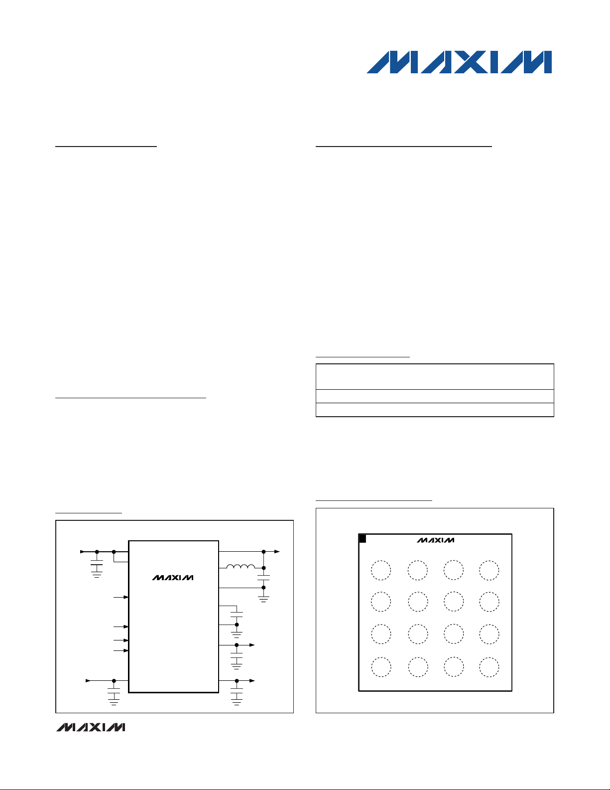
2–4MHz
BUCK
FB
REF
LDO1
CONTROL
LX
2.2μH (MAX8884Y)
1.0μH (MAX8884Z)
PGND
IN1A
SEL
REFBP
AGND
LDO1
LDO2
IN2
GPIO
GPIO
GPIO
BASEBAND
PROCESSOR
CAMERA MODULE
CORE
DIGITAL
ANALOG
1.2V
IN1B
LDO2_EN
LDO1_EN
BUCK_EN
4.7μF
Li+
BATTERY
2.2μF
2.2μF
2.2μF
2.2μF
0.033μF
MAX8884Y
MAX8884Z
LDO2
Typical Application Circuit
 Loading...