

Page 1
_______________General Description
The MAX887 high-efficiency, step-down DC-DC converter provides an adjustable output from 1.25V to
10.5V. It accepts inputs from 3.5V to 11V and delivers
600mA. Operation to 100% duty cycle minimizes
dropout voltage (300mV typ at 500mA). Synchronous
rectification reduces output rectifier losses, resulting in
efficiency as high as 95%.
Fixed-frequency pulse-width modulation (PWM)
reduces noise in sensitive communications applications. Using a high-frequency internal oscillator allows
tiny surface-mount components to reduce PC board
area, and eliminates audio-frequency interference. A
SYNC input allows synchronization to an external clock
to avoid interference with sensitive RF and dataacquisition circuits.
The MAX887 features current-mode operation for superior load/line-transient response. Cycle-by-cycle current
limiting protects the internal MOSFET and rectifier. A
low-current (2.5µA typ) shutdown mode conserves battery life.
________________________Applications
Portable Instruments
Cellular Phones and Radios
Personal Communicators
Distributed Power Systems
Computer Peripherals
____________________________Features
♦ 95% Efficiency
♦ 600mA Output Current
♦ Cycle-by-Cycle Current Limiting
♦ Low-Dropout, 100% Duty-Cycle Operation,
300mV at 500mA
♦ Internal 0.6Ω (typ) MOSFET
♦ Internal Synchronous Rectifier
♦ High-Frequency Current-Mode PWM
♦ External SYNC or Internal 300kHz Oscillator
♦ Guaranteed 260kHz to 340kHz Internal Oscillator
Frequency Limits
♦ 2.5µA Shutdown Mode
MAX887
100% Duty Cycle, Low-Noise,
Step-Down, PWM DC-DC Converter
________________________________________________________________
Maxim Integrated Products
1
1
2
8
7
V+
LX
SYNC
GND
SHDN
FB
REF
VL
MAX887
SO
TOP VIEW
3
4
6
5
__________________Pin Configuration
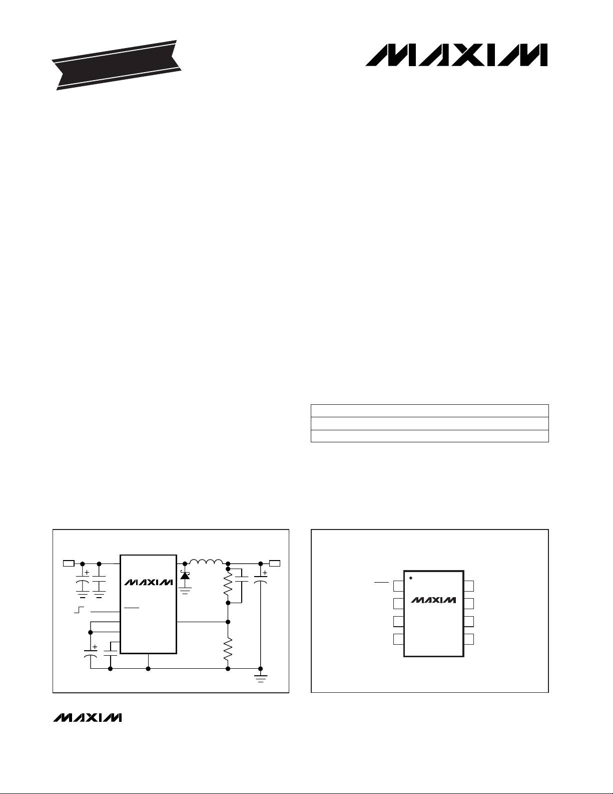
MAX887
REF
R1
165kΩ
R2
100kΩ
0.047µF
2.2µF
47µF
47µF
C1
100pF
0.33µF
33µH
V+ LX
FB
GND
SYNC
VL
SHDN
V
OUT
= 3.3V
V
OUT
= 1.25V (R1/R2 + 1)
V
IN
= 3.5V to 11V
ON
OFF
__________Typical Operating Circuit
19-1142 Rev 0; 9/96
PART
MAX887HC/D
MAX887HESA -40°C to +85°C
0°C to +70°C
TEMP. RANGE PIN-PACKAGE
Dice*
8 SO
EVALUATION KIT MANUAL
AVAILABLE
______________Ordering Information
*
Contact factory for availability. Dice are tested at TA= +25°C.
For free samples & the latest literature: http://www.maxim-ic.com, or phone 1-800-998-8800
Page 2
100% Duty Cycle, Low-Noise,
Step-Down, PWM DC-DC Converter
ABSOLUTE MAXIMUM RATINGS
REF, FB, SYNC, VL to GND..................................... -0.3V to +6V
V+ to GND............................................................. -0.3V to +12V
SHDN, LX to GND ....................................... -0.3V to (V+ + 0.3V)
PGND to GND ......................................................-0.3V to +0.3V
Continuous Power Dissipation (T
SO (derate 9.09mW/°C above +70°C) .........................471mW
Stresses beyond those listed under “Absolute Maximum Ratings” may cause permanent damage to the device. These are stress ratings only, and functional
MAX887
operation of the device at these or any other conditions beyond those indicated in the operational sections of the specifications is not implied. Exposure to
absolute maximum rating conditions for extended periods may affect device reliability.
= +70°C)
A
ELECTRICAL CHARACTERISTICS
(V+ = +7V, PGND = GND = 0V, SHDN = V+, (TA= 0°C to T
Quiescent Supply Current
(PWM Mode)
Quiescent Supply Current
(PFM Mode)
Shutdown Supply Current
Output Voltage Range
PWM FB Feedback Threshold
FB Input Current
SYNC Frequency
PWM Switching Frequency
High-Side Current Limit
LX On-Resistance
LX Leakage Current
LX Reverse Leakage Current,
Regulator Off
Undervoltage Lockout
Startup Voltage
SYNC Input High Voltage
SYNC Input Low Voltage
SYNC Input Current
SHDN Input High Voltage
SHDN Input Low Voltage
SHDN Input Current, Sinking
SHDN Input Capacitance
VL Output Voltage V
REF Output Voltage V
Note 1: Guaranteed by design and not production tested.
V+, PWM
V+, PFM
V+, SHDN
OUT, RANGE
FB
FB
SYNC
OSC
LIM+
ON, LX
LXLKG
LXLKGR
+, UVLO
+, START
IH, SYNC
IL, SYNC
IN, SYNC
IH, SHDN
V
IL, SHDN
I
IN-, SHDN
C
IN, SHDN
L
REF
I
I
SHDN = GND
Circuit of Figure 2
I
VIN= 4V to 11V, PWM mode
SYNC = 3.0V, PWM duty cycle = 50%
FB = 1.30V
SYNC = 3.0V, FB = 1.18V
SYNC = 3.0V
ILX= ±100mA
V+ = 12V, LX = GND to 12V
V+ = floating, LX = 5V, SHDN = GND
V+ falling
V+ rising
SYNC = GND or 3V
SHDN = GND or V+
(Note 1) 10 pF
IVL= 0mA to 1mA 3.3 V
0µA to 30µA 1.25 V
MAX
= 0mA, SYNC = 3.0V
OUT
= 0mA, SYNC = GND
OUT
= 0mA to 500mA
OUT
Operating Temperature Ranges
MAX887HC/D.......................................................0°C to +70°C
MAX887HESA...................................................-40°C to +85°C
Storage Temperature Range ........................... -65°C to +165°C
Lead Temperature (soldering, 10sec)............................ +300°C
), unless otherwise noted.)
CONDITIONS
0.8 V
±1 µA
UNITSMIN TYP MAXSYMBOLPARAMETER
%/mA0.005Load Regulation
%/V0.2Line Regulation
kHz25 440f
kHz260 300 340f
V3.5 11.0V+Supply Range
mA2.7 4.0I
mA0.2 0.5I
µA2.5 5I
V1.25 10.50V
V1.225 1.250 1.275V
µA±0.10I
ns500SYNC, PWSYNC Pulse Width High or Low
%100PWM, DUTYPWM Maximum Duty Cycle
A0.75 1.0 1.40I
Ω0.6R
µA-10 1.0 10I
µA1.0 20I
V3.0 3.3V
V3.1 3.5V
V2.5V
V0.5V
µA±1I
V2.4V
2 _______________________________________________________________________________________
Page 3
100% Duty Cycle, Low-Noise,
Step-Down, PWM DC-DC Converter
ELECTRICAL CHARACTERISTICS
(V+ = +7V, PGND = GND = 0V, SHDN = V+, (TA= -40°C to +85°C), unless otherwise noted.) (Note 2)
CONDITIONS
Quiescent Supply Current
(PWM Mode)
Quiescent Supply Current
(PFM Mode)
Shutdown Supply Current
Output Voltage Range
PWM FB Feedback Threshold
FB Input Current
PWM Switching Frequency
High-Side Current Limit
Undervoltage Lockout
Startup Voltage
V+, PWM
V+, PFM
V+, SHDN
OUT, RANGE
FB
FB
OSC
LIM+
+, UVLO
+, START
Note 2: Specifications from 0°C to -40°C are guaranteed by design and not production tested.
I
= 0mA, SYNC = 3.0V
OUT
I
= 0mA, SYNC = GND
OUT
SHDN = GND
Circuit of Figure 2
SYNC = 3.0V, PWM duty cycle = 50%
FB = 1.30V
SYNC = 3.0V
V+ falling
V+ rising
MAX887
UNITSMIN TYP MAXSYMBOLPARAMETER
V3.5 11.0V+Supply Range
mA2.7 4.0I
mA0.2 0.6I
µA2.5 5I
V1.25 10.50V
V1.222 1.250 1.278V
µA±0.10I
kHz250 300 350f
A0.75 1.00 1.50I
V3.0 3.3V
V3.1 3.5V
__________________________________________Typical Operating Characteristics
(Circuit of Figure 2, TA = +25°C, unless otherwise noted.)
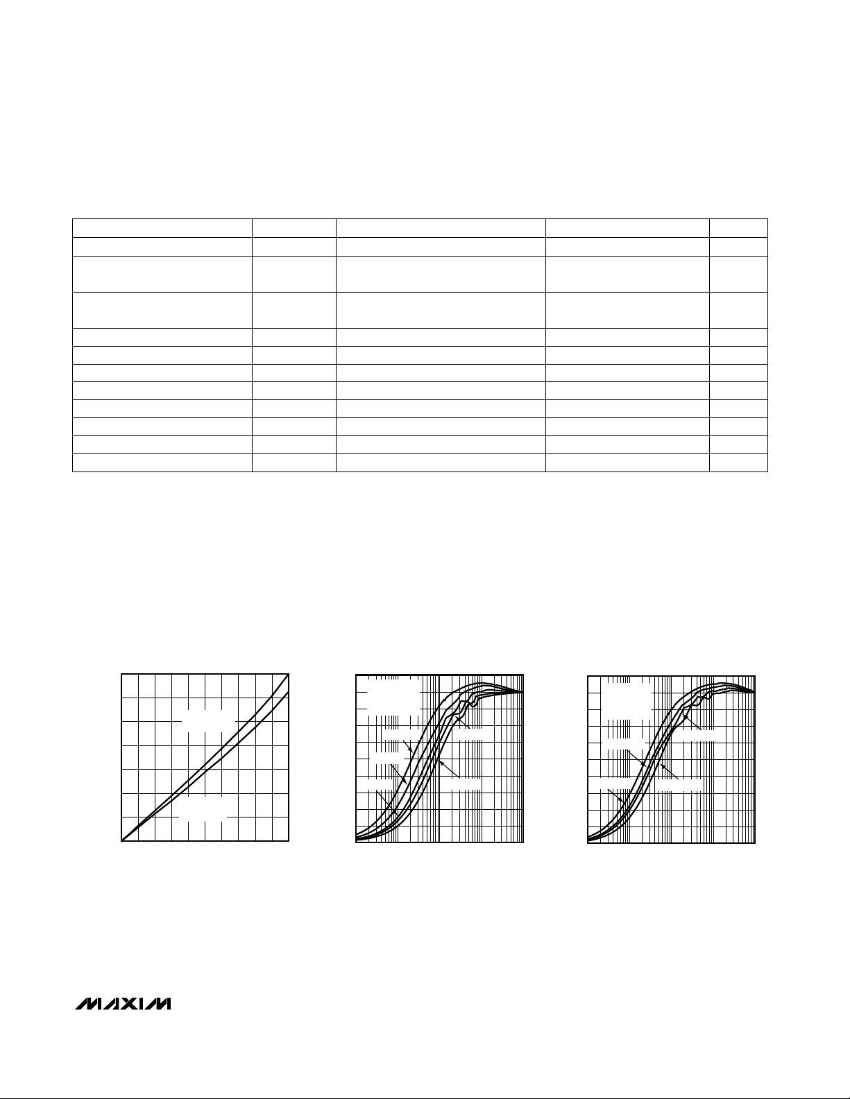
DROPOUT VOLTAGE
vs. LOAD CURRENT
0.7
0.6
0.5
0.4
0.3
DROPOUT VOLTAGE (V)
0.2
0.1
0
0 200 400 600 800 1000
3.3V SETTING
= 3.135V
V
OUT
5V SETTING
= 4.75V
V
OUT
LOAD CURRENT (mA)
MAX887-01
EFFICIENCY vs. OUTPUT CURRENT
100
PWM MODE
90
(SYNC = VL)
= 3.3V
V
80
70
60
50
40
EFFICIENCY (%)
30
20
10
OUT
V
V
= 11V
IN
IN
= 9V
VIN = 4V
= 5V
V
IN
V
= 7V
IN
0
0.0001 0.001 0.01 0.1 0.6
OUTPUT CURRENT (A)
MAX887-02
EFFICIENCY (%)
EFFICIENCY vs. OUTPUT CURRENT
100
PWM MODE
90
(SYNC = VL)
80
70
60
50
40
30
20
10
0
0.0001 0.001 0.01 0.1 0.6
V
OUT
VIN = 7V
VIN = 5.5V
= 5V
VIN = 9V
= 11V
V
IN
OUTPUT CURRENT (A)
MAX887-03
_______________________________________________________________________________________ 3
Page 4
100% Duty Cycle, Low-Noise,
Step-Down, PWM DC-DC Converter
____________________________Typical Operating Characteristics (continued)
(Circuit of Figure 2, TA = +25°C, unless otherwise noted.)
EFFICIENCY vs. OUTPUT CURRENT
100
MAX887
EFFICIENCY (%)
VIN = 4V
90
80
VIN = 5V
70
60
50
40
30
20
10
0
0.0001 0.001 0.01 0.1 0.6
VIN = 9V
VIN = 7V
OUTPUT CURRENT (A)
MAXIMUM OUTPUT CURRENT
vs. SYNC FREQUENCY
1200
1000
800
600
400
200
MAXIMUM OUTPUT CURRENT (mA)
0
0 100 200 300 400 500 600
VIN = 11V
IDLE MODE
(SYNC = GND)
V
OUT
C2, C3 = 47µF
L1 = 33µH
= 5V
V
IN
= 3.3V
V
OUT
= -5% at I
V
OUT
SYNC FREQUENCY (kHz)
= 3.3V
OUT(MAX)
100
90
MAX887-04
80
70
60
50
40
EFFICIENCY (%)
30
20
10
0
0.0001 0.001 0.01 0.1 0.6
3.5
MAX887-07
3.0
2.5
2.0
1.5
1.0
QUIESCENT CURRENT (mA)
0.5
0
EFFICIENCY vs. OUTPUT CURRENT
VIN = 5.5V
VIN = 11V
VIN = 9V
VIN = 7V
OUTPUT CURRENT (A)
IDLE MODE
(SYNC = GND)
= 5V
V
OUT
QUIESCENT SUPPLY CURRENT
vs. SUPPLY VOLTAGE
A
A
A: V
= 3.3V, PWM MODE
OUT
= 3.3V, PFM MODE
B: V
OUT
C
B
024681012141618
SUPPLY VOLTAGE (V)
MAXIMUM OUTPUT CURRENT
1200
MAX887-05
1000
800
600
400
200
MAXIMUM OUTPUT CURRENT (mA)
MAX887-08
QUIESCENT CURRENT (mA)
GUARANTEED OUTPUT CURRENT
OF FIGURE 2 IS 600mA
0
357911131517
3.0
VIN = 5.3V
= 3.3V
V
OUT
2.5
2.0
1.5
1.0
0.5
0
-60 -40 -20 0 20 40 60 80 100 120 140
vs. SUPPLY VOLTAGE
3.3V SETTING, V
5V SETTING, V
SUPPLY VOLTAGE (V)
OUT
OUT
= 3.135V
= 4.75V
QUIESCENT CURRENT
vs.TEMPERATURE
PWM MODE
PFM MODE
TEMPERATURE (°C)
MAX887-06
MAX887-09
SWITCHING FREQUENCY
vs. SUPPLY VOLTAGE
350
V
= 3.3V
340
330
320
310
300
290
280
270
SWITCHING FREQUENCY (kHz)
260
250
OUT
024681012141618
SUPPLY VOLTAGE (V)
350
340
MAX887-10
330
320
310
300
290
FREQUENCY (kHz)
280
270
260
250
SWITCHING FREQUENCY
vs. TEMPERATURE
V
= 3.3V
OUT
-60 -40 -20 0 20 40 60 80 100 120 140
TEMPERATURE (°C)
MAX887-11
OUTPUT NOISE (mV)
OUTPUT RIPPLE AND HARMONICS
4
VIN = 5V
= 3.3V
V
OUT
= 500mA
I
3
OUT
PWM MODE
2
1
0
-1
10k 10M
100k 1M
FREQUENCY (Hz)
4 _______________________________________________________________________________________
MAX887 TOC-20
Page 5

100% Duty Cycle, Low-Noise,
Step-Down, PWM DC-DC Converter
____________________________Typical Operating Characteristics (continued)
(Circuit of Figure 2, TA = +25°C, unless otherwise noted.)
LIGHT-LOAD, PWM-MODE
SWITCHING WAVEFORMS
A
B
C
VIN = 5V, V
OUT
A: LX, 5V/div
B: V
, 20mV/div, AC COUPLED
OUT
C: INDUCTOR CURRENT, 500mA/div
MAX887-13
1µs/div
= 3.3V, LOAD = 0mA
0mA
HEAVY-LOAD, PWM-MODE
SWITCHING WAVEFORMS
A
B
C
VIN = 5V, V
OUT
A: LX, 5V/div
B: V
, 20mV/div, AC COUPLED
OUT
C: INDUCTOR CURRENT, 500mA/div
MAX887-12
1µs/div
= 3.3V, LOAD = 500mA
MAX887
LIGHT-LOAD, PFM-MODE
SWITCHING WAVEFORMS
A
B
C
VIN = 5V, V
A: LX, 5V/div
B: V
, 20mV/div, AC COUPLED
OUT
C: INDUCTOR CURRENT, 200mA/div
1µs/div
= 3.3V, LOAD = 0mA
OUT
MAX887-14
MEDIUM-LOAD, PFM-MODE
SWITCHING WAVEFORMS
A
B
C
VIN = 5V, V
OUT
A: LX, 5V/div
B: V
, 20mV/div, AC COUPLED
OUT
C: INDUCTOR CURRENT, 200mA/div
MAX887-15
10µs/div
= 3.3V, LOAD = 70mA
_______________________________________________________________________________________
5
Page 6

100% Duty Cycle, Low-Noise,
Step-Down, PWM DC-DC Converter
_____________________________Typical Operating Characteristics (continued)
(Circuit of Figure 2, TA = +25°C, unless otherwise noted.)
MAX887
A
B
C
LOAD-TRANSIENT RESPONSE
40µs/div
V
= 5V, V
IN
LOAD = 0mA TO 500mA, PWM MODE
A: LX, 5V/div
B: V
C: LOAD CURRENT, 500mA/div
= 3.3V,
OUT
, 50mV/div, AC COUPLED
OUT
RECOVERY FROM 100% DUTY CYCLE
(DROP OUT)
MAX887-16
LINE-TRANSIENT RESPONSE
A
B
200µs/div
= 5V TO 11V, V
V
IN
LOAD = 500mA, PWM MODE
A: V
, 5V/div
IN
B: V
, 20mV/div, AC COUPLED
OUT
OUT
= 3.3V,
SHUTDOWN AND STARTUP RESPONSE
MAX887-17
A
B
C
D
V
= 5V, V
IN
OUT
LOAD = 100mA, PWM MODE
A: SHDN, 5V/div
B: V
, 2V/div, AC COUPLED
OUT
C: LX, 5V/div
D: INDUCTOR CURRENT, 500mA/div
500µs/div
= 3.3V,
A
B
C
= 3.3V TO 11V, V
V
IN
LOAD = 500mA, PWM MODE
A: V
IN
B: V
OUT
C: LX, 10V/div
200µs/div
= 3.3V,
OUT
, 5V/div
, 50mV/div, AC COUPLED
MAX887-18
6 _______________________________________________________________________________________
MAX887-19
Page 7

100% Duty Cycle, Low-Noise,
Step-Down, PWM DC-DC Converter
______________________________________________________________Pin Description
PIN
1
2 FB Feedback Input. Connect FB to a resistor voltage divider between the output and GND.
3 REF Reference Bypass Output. Connect a 0.047µF capacitor to GND very close to the MAX887, within 0.2 in. (5mm).
4 VL
5 GND Ground
6 SYNC
7 LX Inductor Connection to the drain of an internal P-channel MOSFET
8 V+
SHDN
VL
REF
NAME FUNCTION
SHDN Shutdown, Active-Low, Logic-Level Input. Connect SHDN to V+ for normal operation.
3.3V Internal Logic Regulator Output. Bypass VL to GND with a 2.2µF capacitor very close to the MAX887,
within 0.2 in. (5mm).
Oscillator Synchronization and PWM Control Input. SYNC is a logic-level input. Tie SYNC to VL for internal
300kHz PWM operation at all loads. The oscillator synchronizes to the negative edge of an external clock
between 10kHz and 400kHz. The MAX887 operates in PWM mode when SYNC is clocked. Tying SYNC to
GND allows a reduced supply-current mode at light loads.
Supply-Voltage Input. 3.5V min to 11V max. Bypass V+ to GND with a 0.33µF and large-value electrolytic
capacitor in parallel. These capacitors must be as close to the V+ and GND pins as possible. Place the
0.33µF capacitor within 0.2 in. (5mm) of the MAX887.
REF
GND
V+
VL
GND
25mV
100mV
PFM CURRENT COMPARATOR
LEVEL
SHIFTER
ILIM COMPARATOR
0.1X
SENSE FET
V+
1Ω
LX
MAX887
RAMP
GEN
SLOPE COMPENSATION
FROM CONTROL LOGIC
PWM
PWM ON
SIGNAL
PFM
COMPARATOR
SYNC
SYNC
CELL
FB
REF
Figure 1. Simplified Functional Block Diagram
_______________________________________________________________________________________ 7
REF
PWM
COMPARATOR
CONTROL &
DRIVER LOGIC
FB
50mV
REF
FB
OVERVOLTAGE
COMPARATOR
NEGLIM
COMPARATOR
0mV in PFM
ADJ. IN PWM
SENSE FET
0.1X
1Ω
GND
Page 8

100% Duty Cycle, Low-Noise,
Step-Down, PWM DC-DC Converter
_______________Detailed Description
The MAX887 is a step-down, pulse-width modulation
(PWM) DC-DC converter that provides an adjustable
output from 1.25V to 10.5V. It accepts inputs from 3.5V
to 11V and delivers up to 600mA. An internal MOSFET
and synchronous rectifier reduce PC board area while
maintaining high efficiency. Cycle-by-cycle current lim-
MAX887
iting protects the internal MOSFETs and reduces system stress during overload conditions. Operation with
up to 100% duty cycle for an output of 3V and higher
minimizes dropout voltage. Fixed-frequency PWM operation reduces interference in sensitive communications
and data-acquisition applications. A SYNC input allows
synchronization to an external clock. When enabled,
Idle Mode™ extends battery life under light loads by
placing the regulator in low quiescent current (200µA
typ) pulse-frequency modulation (PFM) operation.
Shutdown quiescent current is 2.5µA typ.
PWM Control Scheme
The MAX887 uses an oscillator-triggered minimum/
maximum on-time current-mode control scheme. The
minimum on-time is approximately 280ns unless in
dropout. The maximum on-time is approximately
4/f
, allowing operation to 100% duty cycle. Current-
OSC
mode feedback provides cycle-by-cycle current limiting for superior load and line response and protection
of the internal MOSFET and rectifier.
At each falling edge of the internal oscillator, the SYNC
cell sends a PWM ON signal to the control and drive
logic, turning on the internal P-channel MOSFET (main
switch) (Figures 1 and 2). This allows current to ramp
up through the inductor (Figure 2) to the load, and
stores energy in a magnetic field. The switch remains
on until either the current-limit (ILIM) comparator is
tripped, the maximum on-time is reached (not shown),
V
= 3.5V to 11V
IN
47µF
OFF
2.2µF
ON
0.33µF
0.047µF
V+ LX
MAX887
SHDN
SYNC
VL
REF
GND
V
= 1.25V (R1/R2 + 1)
OUT
33µH
R1
165kΩ
FB
R2
100kΩ
V
OUT
C1
100pF
= 3.3V
47µF
or the PWM comparator signals that the output is in
regulation. When the switch turns off, during the second half of each cycle, the inductor’s magnetic field
collapses, releasing the stored energy and forcing current through the output diode to the output filter capacitor and load. The output filter capacitor stores charge
when the inductor current is high and releases it when
the inductor current is low, smoothing the voltage
across the load.
During normal operation, the MAX887 regulates output
voltage by switching at a constant frequency and then
modulating the power transferred to the load per pulse
using the PWM comparator. A multi-input comparator
sums three weighted differential signals (the output
voltage with respect to the reference, the main switch
current sense, and the slope-compensation ramp) and
changes states when a threshold is reached. It modulates
output power by adjusting the inductor peak current
during the first half of each cycle, based on the output
error voltage. The MAX887’s loop gain is relatively low
to enable the use of a small, low-valued output filter
capacitor. The resulting load regulation is 2.5% typ at
500mA. Slope compensation is added to account for
the inductor current waveform’s down slope during the
second half of each cycle, and to eliminate the inductor
current staircasing characteristic of current-mode controllers at high duty cycles.
100% Duty-Cycle Operation
For the internal oscillator frequency, the f
mum on-time exceeds one cycle and permits operation
to 100% duty cycle. As the input voltage drops, the
duty cycle increases until the P-channel MOSFET is
held on continuously and 100% duty cycle is reached.
Dropout voltage in 100% duty cycle is the output current multiplied by the on-resistance of the internal
switch and inductor around 300mV (I
OUT
PWM mode, subharmonic oscillation can occur near
dropout, but subharmonic voltage ripple is small, since
the ripple current is low. When using synchronization to
an external oscillator, 100% duty cycle is available for
SYNC frequencies higher than f
OSC
/4.
/4 maxi-
OSC
= 500mA). In
Synchronous Rectification
Although an external Schottky diode is used as the primary output rectifier, an N-channel synchronous rectifier turns on to reduce power loss across the diode and
improve efficiency. During the second half of each
cycle, when the inductor current ramps below the
threshold set by the NEGLIM comparator or when the
end of the oscillator period is reached, the synchronous
rectifier turns off. This keeps excess current from flowing
Figure 2. Typical Operating Circuit
8 _______________________________________________________________________________________
Page 9

100% Duty Cycle, Low-Noise,
Step-Down, PWM DC-DC Converter
backward through the inductor, from the output filter
capacitor to GND, or through the switch and synchronous rectifier to GND.
During PWM operation, the NEGLIM threshold adjusts
to permit small amounts of reverse current to flow from
the output during light loads. This allows regulation with
a constant switching frequency and eliminates minimum load requirements. The NEGLIM comparator
threshold is 0mA if VFB < 1.25V, and decreases as VFB
exceeds 1.25V to prevent the output from rising. The
NEGLIM threshold in PFM mode is 0mA. (See
PWM and Idle Mode operation.
)
Forced
Forced PWM and Idle Mode Operation
Connect SYNC to VL for normal forced PWM operation.
Forced PWM operation is desirable in sensitive RF and
data-acquisition applications, to ensure that switchingnoise harmonics do not interfere with sensitive IF and
data-sampling frequencies. A minimum load is not
required during forced PWM operation, since the synchronous rectifier passes reverse inductor current as
needed to allow constant-frequency operation with no
load.
Connecting SYNC to GND enables Idle Mode operation. This proprietary control scheme places the
MAX887 in PFM mode at light loads to improve efficiency and reduce quiescent current to 200µA typ. With
Idle Mode enabled, the MAX887 initiates PFM operation
when the output current drops below 100mA. During
PFM operation, the MAX887 switches only as needed
to service the load, reducing the switching frequency
and associated losses in the internal switch and
synchronous rectifier, Schottky diode, and external
inductor.
During PFM mode, a switching cycle is initiated when
the PFM comparator senses that the output voltage has
dropped too low. The P-channel MOSFET switch turns
on and conducts current to the output filter capacitor
and load until the inductor current reaches the PFM
peak current limit (100mA). Then the switch turns off
and the magnetic field in the inductor collapses, forcing
current through the output diode to the output filter
capacitor and load. The output filter capacitor stores
charge when the inductor current is high and releases
charge when it is low, smoothing the voltage across the
load. Then the MAX887 waits until the PFM comparator
senses a low output voltage again. During PFM mode,
the synchronous rectifier is disabled and the external
Schottky diode is used as an output rectifier.
The PFM current comparator controls both entry into
PWM mode and the peak switching current during PFM
mode. Consequently, some jitter is normal during tran-
sition from PFM to PWM modes with loads around
100mA, and has no adverse impact on regulation.
Output ripple is higher during PFM operation, and the
output filter capacitor should be selected on this basis
when PFM mode is used. Output ripple and noise are
higher during PFM operation.
SYNC Input and Frequency Control
The MAX887H comes with an internal oscillator set for a
fixed switching frequency of 300kHz. Connect SYNC to
VL for normal forced-PWM operation. Do not leave
SYNC floating. Connecting SYNC to GND enables Idle
Mode operation to reduce supply current at light loads.
SYNC is a logic-level input useful for operating-mode
selection and frequency control. It is a negative edge
triggered input that allows synchronization to an external frequency between 25kHz and 440kHz. When
SYNC is clocked by an external signal, the converter
operates in PWM mode. If SYNC is low or high for more
than 100µs, the oscillator defaults to 300kHz. Operating
at a lower switching frequency reduces quiescent current, but reduces maximum load current as well
(Table 1). For example, at 330kHz, maximum output
current is 600mA, while at 30kHz, maximum output current is only 30mA. Note that 100% duty cycle will only
occur for f
SYNC
> f
OSC
/4.
VL Regulator
The MAX887 uses an internal 3.3V linear regulator for
logic power in the IC. This logic supply is brought out
using the VL pin for bypassing and compensation with
an external 2.2µF capacitor to GND. Connect this
capacitor close to the MAX887, within 0.2in (5mm).
Shutdown
Connecting SHDN to GND places the MAX887 in a lowcurrent shutdown mode (IQ= 2.5µA typ at V+ = 7V). In
shutdown, the reference, VL regulator, control circuitry,
internal switching MOSFET, and the synchronous rectifier turn off and the output falls to 0V. Connect SHDN to
V+ for normal operation.
Current-Sense Comparators
Several internal current-sense comparators are used
inside the MAX887. In PWM operation, the PWM comparator is used for current-mode control. Current-mode
control imparts cycle-by-cycle current limiting and provides improved load and line response, allowing tighter
specification of the inductor saturation current limit to
reduce inductor cost. A second 100mA current-sense
comparator is used across the P-channel switch to control entry into PFM mode. A third current-sense comparator monitors current through the internal N-channel
MOSFET to set the NEGLIM threshold and determine
MAX887
_______________________________________________________________________________________ 9
Page 10

100% Duty Cycle, Low-Noise,
Step-Down, PWM DC-DC Converter
when to turn off this synchronous rectifier. A fourth
comparator (ILIM) is used at the P-channel MOSFET
switch for overcurrent detection. This protects the system, external components, and internal MOSFETs
under overload conditions.
________________Design Information
MAX887
To select an output voltage between 1.25V and 10.5V,
connect FB to a resistor voltage divider between the
output and GND (Figure 2). Select feedback resistor R2
in the 5kΩ to 100kΩ range, since FB input leakage is
±100nA max. R1 is then given by:
R1 R2
where VFB= 1.25V. A small ceramic capacitor (C1)
around 100pF to 470pF should be added in parallel
with R1 to compensate for stray capacitance at the FB
pin, and output capacitor equivalent series resistance
(ESR).
A 1.3A inductor with the value recommended in Table 1
is sufficient for most applications. However, the exact
inductor value is not critical, and values within 50% of
those in Table 1 are acceptable. For best efficiency, the
inductor’s DC resistance should be less than 0.25Ω.
The inductor saturation current rating must exceed the
1A I
Input and output filter capacitors should be chosen to
service inductor currents with acceptable voltage ripple. The input filter capacitor also reduces peak currents and noise at the voltage source. See Table 1 for
suggested values. The MAX887’s loop gain is relatively
low, to enable the use of small, low-valued output filter
capacitors. Higher values provide improved output rip-
Table 1. Inductor and Output Filter
vs. Sync Frequency
current limit. Table 2 lists component suppliers.
LIM
SYNC
RANGE (kHz)
300–400 33 33
200–300 47 47
150–200 68 68
100–150 100 100
75–100 150 150
Output Voltage Selection
V
=−
OUT
V
FB
1
Inductor Selection
Capacitor Selection
L1
(µH)
C
(µF)
OUT
ple and transient response. Lower oscillator frequencies require a larger-value output capacitor. When Idle
Mode is used, verify capacitor selection with light loads
during PFM operation, since output ripple is higher
under these conditions.
Low-ESR capacitors are recommended. Capacitor ESR
is a major contributor to output ripple (usually more
than 60%). Ordinary aluminum-electrolytic capacitors
have high ESR and should be avoided. Low-ESR aluminum-electrolytic capacitors are acceptable and relatively inexpensive. Low-ESR tantalum capacitors
are better and provide a compact solution for spaceconstrained surface-mount designs. Do not exceed
the ripple current ratings of tantalum capacitors.
Ceramic capacitors have the lowest ESR overall, and
OS-CON capacitors have the lowest ESR of the highvalue electrolytic types. It is generally not necessary to
use ceramic and OS-CON capacitors for the MAX887;
they need only be considered in very compact, highreliability, or wide-temperature applications, where the
expense is justified. When using very-low-ESR capacitors, such as ceramic or OS-CON, check for stability
while examining load-transient response, and increase
the compensation capacitor C1 if needed. Table 2 lists
suppliers for the various components used with the
MAX887.
Table 2. Component Suppliers
COMPANY PHONE FAX
AVX USA (803) 946-0690 (803) 626-3123
(800) 282-4975
Coilcraft USA (847) 639-6400 (847) 639-1469
Coiltronics USA (561) 241-7876 (561) 241-9339
Dale USA (605) 668-4131 (605) 665-1627
International USA (310) 322-3331 (310) 322-3332
Rectifier
Motorola USA (602) 303-5454 (602) 994-6430
Nichicon USA (847) 843-7500 (847) 843-2798
Japan 81-7-5231-8461 81-7-5256-4158
Nihon USA (805) 867-2555 (805) 867-2698
Japan 81-3-3494-7411 81-3-3494-7414
Sanyo USA (619) 661-6835 (619) 661-1055
Japan 81-7-2070-6306 81-7-2070-1174
Siliconix USA (408) 988-8000 (408) 970-3950
(800) 554-5565
Sprague USA (603) 224-1961 (603) 224-1430
Sumida USA (847) 956-0666 (847) 956-0702
Japan 81-3-3607-5111 81-3-3607-5144
United USA (714) 255-9500 (714) 255-9400
Chemi-Con
10 ______________________________________________________________________________________
Page 11

100% Duty Cycle, Low-Noise,
Step-Down, PWM DC-DC Converter
Bypass V+ to GND using a 0.33µF capacitor. Also
bypass VL to GND with a 2.2µF capacitor, and VREF to
GND using a 0.047µF capacitor. These capacitors
should be placed within 0.2in (5mm) of their respective
pins. A small ceramic capacitor (C1) of around 100pF
to 470pF should be added in parallel with R1 to compensate for stray capacitance at the FB pin and output
capacitor ESR.
Output Diode Selection
A 1A external diode (D1) is required as an output rectifier to pass inductor current during the second half of
each cycle. This diode operates in PFM mode and during transition periods while the synchronous rectifier is
off. Use a Schottky diode to prevent the slow internal
diode of the N-channel MOSFET from turning on.
PC Board Layout and Routing
High switching frequencies and large peak currents
make PC board layout a very important part of design.
Poor design can result in excessive EMI on the feedback paths and voltage gradients in the ground plane,
both of which can result in instability or regulation
errors. Power components, such as the MAX887,
inductor, input filter capacitor, and output filter capacitor should be placed as close together as possible,
and their traces kept short, direct, and wide. Connect
their ground pins at a common node in a star-ground
configuration. Keep the extra copper on the board and
integrate into ground as a pseudo-ground plane. The
external voltage-feedback network should be very
close to the FB pin, within 0.2in (5mm). Keep noisy
traces, such as from the LX pin, away from the voltagefeedback network, and separate using grounded copper. Place the small bypass capacitors (C1, C3, C5,
and C6) within 0.2in (5mm) of their respective pins. The
MAX887 evaluation kit manual illustrates an example
PC board layout, routing, and pseudo-ground plane.
___________________Chip Information
TRANSISTOR COUNT: 2006
SUBSTRATE CONNECTED TO GND
MAX887
______________________________________________________________________________________ 11
Page 12

100% Duty Cycle, Low-Noise,
Step-Down, PWM DC-DC Converter
________________________________________________________Package Information
MAX887
e
DIM
D
A
0.101mm
0.004in.
A1
B
C
L
0°-8°
Narrow SO
HE
SMALL-OUTLINE
PACKAGE
(0.150 in.)
A
A1
B
C
E
e
H
L
DIM
D
D
D
INCHES MILLIMETERS
MIN
0.053
0.004
0.014
0.007
0.150
0.228
0.016
PINS
8
14
16
MAX
0.069
0.010
0.019
0.010
0.157
0.244
0.050
INCHES MILLIMETERS
MIN
MAX
0.189
0.197
0.337
0.344
0.386
0.394
MIN
1.35
0.10
0.35
0.19
3.80
5.80
0.40
MIN
4.80
8.55
9.80
1.270.050
MAX
1.75
0.25
0.49
0.25
4.00
6.20
1.27
MAX
5.00
8.75
10.00
21-0041A
12 ______________________________________________________________________________________
 Loading...