

Page 1
General Description
The MAX8840/MAX8841/MAX8842 ultra-low-noise, lowdropout (LDO) linear regulators are designed to deliver
up to 150mA continuous output current. These regulators achieve a low 120mV dropout for 120mA load current. The MAX8840 uses an advanced architecture to
achieve ultra-low output voltage noise of 11µV
RMS
and
PSRR of 54dB at 100kHz.
The MAX8841 does not require a bypass capacitor,
hence achieving the smallest PC board area. The
MAX8842 output voltage can be adjusted with an external divider.
The MAX8840/MAX8841 are preset to a variety of voltages in the 1.5V to 4.5V range. Designed with a p-channel
MOSFET series pass transistor, the MAX8840/MAX8841/
MAX8842 maintain very low ground current (40µA).
The regulators are designed and optimized to work with
low-value, low-cost ceramic capacitors. The MAX8840
requires only 1µF (typ) of output capacitance for stability
with any load. When disabled, current consumption drops
to below 1µA.
The MAX8840/MAX8841/MAX8842 are available in a tiny
1mm x 1.5mm x 0.8mm µDFN.
Applications
Cellular and Cordless Phones
PDA and Palmtop Computers
Base Stations
Bluetooth Portable Radios and Accessories
Wireless LANs
Digital Cameras
Personal Stereos
Portable and Battery-Powered Equipment
Features
♦ Space-Saving 1.0mm x 1.5mm x 0.8mm µDFN
♦ 11µV
RMS
Output Noise at 100Hz to 100kHz
Bandwidth (MAX8840)
♦ 78dB PSRR at 1kHz (MAX8840)
♦ 120mV Dropout at 120mA Load
♦ Stable with 1µF Ceramic Capacitor for Any Load
♦ Guaranteed 150mA Output
♦ Only Need Input and Output Capacitors (MAX8841)
♦ Output Voltages: 1.5V, 1.8V, 2.5V, 2.6V, 2.7V, 2.8V,
2.85V, 3V, 3.3V, 4.5V (MAX8840/MAX8841) and
Adjustable (MAX8842)
♦ Low 40µA Ground Current
♦ Excellent Load/Line Transient
♦ Overcurrent and Thermal Protection
MAX8840/MAX8841/MAX8842
Ultra-Low-Noise, High PSRR, Low-Dropout,
150mA Linear Regulators in µDFN
________________________________________________________________ Maxim Integrated Products 1
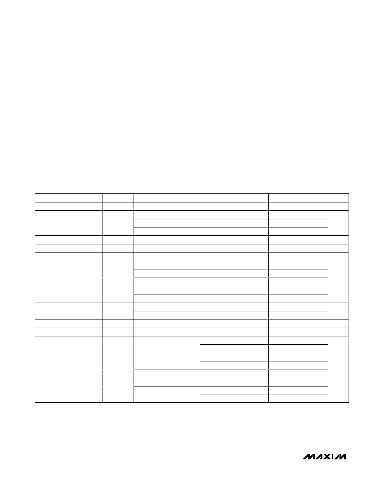
Pin Configuration
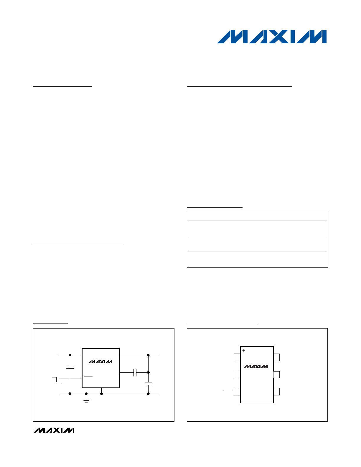
Ordering Information
MAX8840
OUTPUT PRESET
1.5V TO 4.5V
IN
INPUT
2V TO 6V
OFF
SHDN
C
BP
10nF
C
OUT
1μF
C
IN
1μF
OUT
ON
BP
GND
Typical Operating Circuits
19-0629; Rev 1; 1/07
For pricing, delivery, and ordering information, please contact Maxim/Dallas Direct! at
1-888-629-4642, or visit Maxim’s website at www.maxim-ic.com.
*xy is the output voltage code (see the Output Voltage Selector
Guide). Other versions between 1.5V and 4.5V are available in
100mV increments. Contact factory for other versions.
+Denotes lead-free package.
Typical Operating Circuits continued at end of data sheet.
Output Voltage Selector Guide appears at end of data sheet.
PART* TEMP RANGE PIN-PACKAGE
MAX8840ELTxy+T -40°C to +85°C
MAX8841ELTxy+T -40°C to +85°C
MAX8842ELT+T -40°C to +85°C
6 µDFN-6
1.5mm x 1.0mm
6 µDFN-6
1.5mm x 1.0mm
6 µDFN-6
1.5mm x 1.0mm
TOP VIEW
1
IN
2
GND
3
SHDN
(1.5mm x 1.0mm)
OUT
6
MAX8840
MAX8841
MAX8842
μDFN
5
N.C.
BP (MAX8840)
N.C. (MAX8841)
4
FB (MAX8842)
Page 2
MAX8840/MAX8841/MAX8842
Ultra-Low-Noise, High PSRR, Low-Dropout,
150mA Linear Regulators in µDFN
2 _______________________________________________________________________________________
ABSOLUTE MAXIMUM RATINGS
ELECTRICAL CHARACTERISTICS
(VIN= V
OUT
+ 0.5V, TA = -40°C to +85°C, unless otherwise noted. CIN= 1µF, C
OUT
= 1µF, C
BP
= 10nF. Typical values are at +25°C;
the MAX8842 is tested with 2.45V output, unless otherwise noted.) (Note 1)
Stresses beyond those listed under “Absolute Maximum Ratings” may cause permanent damage to the device. These are stress ratings only, and functional
operation of the device at these or any other conditions beyond those indicated in the operational sections of the specifications is not implied. Exposure to
absolute maximum rating conditions for extended periods may affect device reliability.
IN to GND .................................................................-0.3V to +7V
Output Short-Circuit Duration ............................................Infinite
OUT, SHDN to GND ......................................-0.3V to (IN + 0.3V)
FB, BP, N.C. to GND..................................-0.3V to (OUT + 0.3V)
Continuous Power Dissipation (T
A
= +70°C)
6-Pin µDFN (derate 2.1mW/°C above +70°C) .............0.168W
θ
JA
..................................................................................477°C/W
Operating Temperature Range ...........................-40°C to +85°C
Junction Temperature......................................................+150°C
Storage Temperature Range .............................-65°C to +150°C
Lead Temperature (soldering, 10s) .................................+300°C
Input Voltage Range V
Maximum Output Current I
Current Limit I
Dropout Voltage (Note 2)
Ground Current I
Line Regulation V
Load Regulation V
Shutdown Supply Current I
Ripple Rejection PSRR
PARAMETER SYMBOL CONDITIONS MIN TYP MAX UNITS
IN
I
= 1mA, TA = +25°C -1 +1
OUT
I
= 100µA to 80mA, TA = +25°C -2 +2Output Voltage Accuracy
OUT
= 100µA to 80mA -3 +3
I
OUT
OUT
LIM
LNR
LDR
SHDN
OUT = 90% of nominal value 150 200 300 mA
V
≥ 3V, I
OUT
V
≥ 3V, I
OUT
2.5V ≤ V
2.5V ≤ V
2V ≤ V
OUT
2V ≤ V
OUT
I
= 0.05mA 40 90
Q
OUT
VIN = V
OUT(nom)
VIN = (V
I
= 1mA to 80mA 0.003 %/mA
OUT
= 80mA 80 170
OUT
= 120mA 120
OUT
< 3V, I
OUT
OUT
< 2.5V, I
< 2.5V, I
< 3V, I
OUT
OUT
OUT
OUT
- 0.1V, I
+ 0.5V) to 6V, I
OUT
SHDN = 0V
f = 1kHz, I
f = 10kHz, I
f = 100kHz, I
OUT
OUT
OUT
= 10mA
= 10mA
= 10mA
26V
150 mA
= 80mA 90 200
= 120mA 135
= 80mA 120 250
= 120mA 180
= 0mA 220 500
OUT
= 0.1mA 0.001 %/V
OUT
TA = +25°C 0.003 1
= +85°C 0.05
T
A
MAX8840 78
MAX8841/MAX8842 72
MAX8840 75
MAX8841/MAX8842 65
MAX8840 54
MAX8841/ MAX8842 46
%
mV
µA
µA
dB
Page 3
MAX8840/MAX8841/MAX8842
Ultra-Low-Noise, High PSRR, Low-Dropout,
150mA Linear Regulators in µDFN
_______________________________________________________________________________________ 3
ELECTRICAL CHARACTERISTICS (continued)
(VIN= V
OUT
+ 0.5V, TA = -40°C to +85°C, unless otherwise noted. CIN= 1µF, C
OUT
= 1µF, C
BP
= 10nF. Typical values are at +25°C;
the MAX8842 is tested with 2.45V output, unless otherwise noted.) (Note 1)
Note 1: Limits are 100% tested at +25°C. Limits over operating temperature range are guaranteed by design.
Note 2: Dropout is defined as V
IN
- V
OUT
when V
OUT
is 100mV below the value of V
OUT
for V
IN
= V
OUT
+ 0.5V.
Note 3: Time needed for V
OUT
to reach 90% of final value.
Typical Operating Characteristics
(VIN= V
OUT
+ 0.5V, CIN= 1µF, C
OUT
= 1µF, CBP= 10nF, TA= +25°C, unless otherwise noted.)
MAX8840
OUTPUT VOLTAGE vs. INPUT VOLTAGE
MAX8840 toc01
INPUT VOLTAGE (V)
OUTPUT VOLTAGE (V)
54321
0.5
1.0
1.5
2.0
2.5
3.0
3.5
0.0
06
I
OUT
= 150mA
I
OUT
= 0mA
MAX8840
OUTPUT VOLTAGE ACCURACY
vs. LOAD CURRENT
MAX8840 toc02
LOAD CURRENT (mA)
% DEVIATION (%)
125100755025
-0.4
-0.2
0
0.2
0.4
0.6
-0.6
0150
MAX8840
OUTPUT VOLTAGE ACCURACY
vs. TEMPERATURE
MAX8840 toc03
TEMPERATURE (°C)
% DEVIATION (%)
603510-15
-0.8
-0.6
-0.4
-0.2
0
0.2
0.4
0.6
0.8
1.0
-1.0
-40 85
I
OUT
= 1mA
Output Noise Voltage
(RMS)
Shutdown Exit Delay R
SHDN Logic-Low Level V
SHDN Logic-High Level V
SHDN Input Bias Current
FB Input Bias Current
(MAX8842)
Thermal Shutdown 160 °C
Thermal-Shutdown
Hysteresis
PARAMETER SYMBOL CONDITIONS MIN TYP MAX UNITS
f = 100Hz to 100kHz,
= 10mA
I
LOAD
f = 100Hz to 100kHz,
= 80mA
I
LOAD
= 50Ω (Note 3) 300 µs
LOAD
= 2V to 6V 0.4 V
IN
= 2V to 6V 1.5 V
IN
V
= 6V, SHDN = 0V or
IN
6V
V
= 6V, V
IN
FB
= 1.3V
MAX8840 11
MAX8841/MAX8842 230
MAX8840 13
MAX8841/MAX8842 230
TA = +25°C
= +85°C 0.01
T
A
TA = +25°C 0.006 0.1
T
= +85°C 0.01
A
10 °C
µV
µA
µA
Page 4

MAX8840/MAX8841/MAX8842
Ultra-Low-Noise, High PSRR, Low-Dropout,
150mA Linear Regulators in µDFN
4 _______________________________________________________________________________________
Typical Operating Characteristics (continued)
(VIN= V
OUT
+ 0.5V, CIN= 1µF, C
OUT
= 1µF, CBP= 10nF, TA= +25°C, unless otherwise noted.)
MAX8440
DROPOUT VOLTAGE vs. LOAD CURRENT
MAX8840 toc04
INPUT VOLTAGE (V)
DROPOUT VOLTAGE (mV)
125100755025
40
20
80
60
120
100
160
140
200
180
0
0 150
TA = +85°C
TA = +25°C
TA = -40°C
MAX8840
DROPOUT VOLTAGE vs. OUTPUT VOLTAGE
MAX8840 toc05
OUTPUT (V)
DROPOUT VOLTAGE (mV)
3.02.82.62.42.2
50
100
150
200
250
0
2.0 3.2
I
OUT
= 80mA
MAX8840
GROUND PIN CURRENT vs. INPUT VOLTAGE
MAX8840 toc06
INPUT VOLTAGE (V)
GROUND PIN CURRENT (μA)
4321
150
200
50
100
250
300
350
0
05
I
LOAD
= 150mA
I
LOAD
= 0mA
MAX8840
GROUND PIN CURRENT vs. LOAD CURRENT
MAX8840 toc 07
LOAD CURRENT (mA)
GROUND PIN CURRENT (μA)
125100755025
100
50
150
200
250
300
350
0
0 150
VIN = 3.8V
VIN = 5.5V
MAX8840
GROUND PIN CURRENT vs. TEMPERATURE
MAX8840 toc08
TEMPERATURE (°C)
GROUND PIN CURRENT (μA)
603510-15
35
40
45
50
30
-40 85
MAX8840
POWER-SUPPLY REJECTION RATIO
vs. FREQUENCY
MAX8840 toc09
FREQUENCY (kHz)
PSRR (dB)
1 10 1000.1
40
50
60
10
20
30
70
80
90
0
0.01 1000
I
LOAD
= 10mA
C
BP
= 10nF
MAX8841
POWER-SUPPLY REJECTION RATIO
vs. FREQUENCY
MAX8840 toc10
FREQUENCY (kHz)
PSRR (dB)
0.1 1 10 100
40
50
60
10
20
30
70
80
90
0
0.01 1000
I
LOAD
= 10mA
MAX8840
OUTPUT NOISE
MAX8840 toc11
400μs/div
VIN = 3.8V
I
LOAD
= 10mA
V
NOISE
= 11μV
RMS
20μV/div
MAX8840
OUTPUT NOISE-SPECTRAL DENSITY
vs. FREQUENCY
MAX8840 toc12
FREQUENCY (kHz)
OUTPUT NOISE DENSITY (nV/√Hz)
0.1 1 10 100
1000
100
10,000
10
0.01 1000
Page 5

MAX8840/MAX8841/MAX8842
Ultra-Low-Noise, High PSRR, Low-Dropout,
150mA Linear Regulators in µDFN
_______________________________________________________________________________________ 5
Typical Operating Characteristics (continued)
(VIN= V
OUT
+ 0.5V, CIN= 1µF, C
OUT
= 1µF, CBP= 10nF, TA= +25°C, unless otherwise noted.)
MAX8840
OUTPUT NOISE vs. BP CAPACITANCE
MAX8840 toc13
BP CAPACITANCE (nF)
OUTPUT NOISE (μV)
10
5
10
15
20
25
0
1 100
MAX8840
LOAD-TRANSIENT RESPONSE
MAX8840 toc14
1ms/div
VIN = 3.5V
I
LOAD
= 0 TO 50mA
V
OUT
10mV/div
MAX8840
LOAD-TRANSIENT RESPONSE NEAR DROPOUT
MAX8840 toc15
1ms/div
VIN = 3.1V
I
LOAD
= 0 TO 50mA
V
OUT
10mV/div
MAX8840
LINE-TRANSIENT RESPONSE
MAX8840 toc16
200μs/div
VIN = 3.5V TO 4V
V
OUT
2mV/div
MAX8840
EXITING SHUTDOWN WAVEFORM
MAX8840 toc17
20μs/div
V
OUT
= 2.85V
R
LOAD
= 47Ω
OUTPUT
VOLTAGE
2V/div
SHUTDOWN
VOLTAGE
MAX8840
ENTERING SHUTDOWN DELAY
MAX8840 toc18
40μs/div
CBP = 0.01μF
OUTPUT
VOLTAGE
2V/div
SHUTDOWN
VOLTAGE
MAX8840
SHUTDOWN EXIT DELAY
MAX8840 toc19
20μs/div
SHUTDOWN
VOLTAGE
V
OUT
1V/div
V
OUT
= 3V
C
BP
= 100nF
MAX8840
REGION OF STABLE C
OUT
ESR
vs. LOAD CURRENT
MAX8840 toc20
LOAD CURRENT (mA)
C
OUT
ESR (Ω)
100755025
0.1
1
10
100
0.01
0 150125
Page 6

MAX8840/MAX8841/MAX8842
Ultra-Low-Noise, High PSRR, Low-Dropout,
150mA Linear Regulators in µDFN
6 _______________________________________________________________________________________
Detailed Description
The MAX8840/MAX8841/MAX8842 are ultra-low-noise,
low-dropout, low-quiescent current linear regulators
designed for space-restricted applications. The parts
are available with preset output voltages ranging from
1.5V to 4.5V. These devices can supply loads up to
150mA. As shown in the Functional Diagram, the
MAX8840/MAX8841 consist of an innovative bandgap
core and noise bypass circuit, error amplifier, p-channel pass transistor, and internal feedback voltagedivider. The MAX8842 allows for adjustable output with
an external feedback network.
The 1.225V bandgap reference is connected to the
error amplifier’s inverting input. The error amplifier compares this reference with the feedback voltage and
amplifies the difference. If the feedback voltage is
lower than the reference voltage, the pass-transistor
gate is pulled low. This allows more current to pass to
the output and increases the output voltage. If the feedback voltage is too high, the pass transistor gate is
pulled high, allowing less current to pass to the output.
The output voltage is fed back through an internal resistor voltage-divider connected to the OUT pin.
An external bypass capacitor connected to BP
(MAX8840) reduces noise at the output. Additional
blocks include a current limiter, thermal sensor, and
shutdown logic.
Internal p-Channel Pass Transistor
The MAX8840/MAX8841/MAX8842 feature a 1Ω (typ)
p-channel MOSFET pass transistor. This provides several advantages over similar designs using a pnp pass
transistor, including longer battery life. The p-channel
MOSFET requires no base drive, which considerably
reduces quiescent current. PNP-based regulators waste
considerable current in dropout when the pass transistor saturates. They also use high base-drive current
under heavy loads. The MAX8840/MAX8841/MAX8842
do not suffer from these problems and consume only
40µA of quiescent current in light load and 220µA in
dropout (see the Typical Operating Characteristics).
Output Voltage Selection
The MAX8840/MAX8841 are supplied with factory-set
output voltages from 1.5V to 4.5V, in 100mV increments
(see the Ordering Information). The MAX8842 features
a user-adjustable output through an external feedback
network (see the Typical Operating Circuits).
To set the output of the MAX8842, use the following
equation:
where R2 is chosen to be less than 240kΩ and V
REF
=
1.225V. Use 1% or better resistors.
Shutdown
The MAX8840/MAX8841/MAX8842 feature a low-power
shutdown mode that reduces quiescent current less
than 1µA. Driving SHDN low disables the voltage reference, error amplifier, gate-drive circuitry, and pass
transistor (see the Functional Diagram), and the device
output enters a high-impedance state. Connect SHDN
to IN for normal operation.
Current Limit
The MAX8840/MAX8841/MAX8842 include a current
limiter, which monitors and controls the pass transistor’s gate voltage, limiting the output current to 200mA.
RRX
V
V
OUT
REF
12 1=
⎛
⎝
⎜
⎞
⎠
⎟
-
Pin Description
PIN
MAX8840 MAX8841 MAX8842
NAME FUNCTION
1 1 1 IN Unregulated Input Supply
2 2 2 GND Ground
333SHDN Shutdown. Pull low to disable the regulator.
4——BP
Noise Bypass for Low-Noise Operation. Connect a 10nF capacitor
from BP to OUT. It is shorted to OUT in shutdown mode.
— — 4 FB Adjustable Output Feedback Point
5 4, 5 5 N.C. No Connection. Not internally connected.
666OUT
Regulated Output Voltage. Bypass with a capacitor to GND. See the
Capacitor Selection and Regulator Stability section.
Page 7

MAX8840/MAX8841/MAX8842
Ultra-Low-Noise, High PSRR, Low-Dropout,
150mA Linear Regulators in µDFN
_______________________________________________________________________________________ 7
For design purposes, consider the current limit to be
150mA (min) to 300mA (max). The output can be shorted
to ground for an indefinite amount of time without damaging the part.
Thermal-Overload Protection
Thermal-overload protection limits total power dissipation
in the MAX8840/MAX8841/MAX8842. When the junction
temperature exceeds TJ= +160°C, the thermal sensor
signals the shutdown logic, turning off the pass transistor
and allowing the IC to cool down. The thermal sensor
turns the pass transistor on again after the IC’s junction
temperature drops by 10°C, resulting in a pulsed output
during continuous thermal-overload conditions.
Thermal-overload protection is designed to protect the
MAX8840/MAX8841/MAX8842 in the event of a fault
condition. For continual operation, do not exceed the
absolute maximum junction temperature rating of TJ =
+150°C.
Operating Region and Power Dissipation
The MAX8840/MAX8841/MAX8842 maximum power
dissipation depends on the thermal resistance of the
case and circuit board, the temperature difference
between the die junction and ambient, and the rate of
airflow. The power dissipation across the device is:
P = I
OUT(VIN
- V
OUT
)
The maximum power dissipation is:
P
MAX
= (TJ- TA) / (θJC+ θCA)
where TJ- TAis the temperature difference between
the MAX8840/MAX8841/MAX8842 die junction and the
surrounding air, θJCis the thermal resistance of the
package, and θCAis the thermal resistance through the
PC board, copper traces, and other materials to the
surrounding air.
The GND pin of the MAX8840/MAX8841/MAX8842 performs the dual function of providing an electrical connection to ground and channeling heat away. Connect
the GND pin to ground using a large pad or ground
plane.
Noise Reduction
For the MAX8840, an external 0.01µF bypass capacitor
between BP and OUT with an innovative noise bypass
scheme reduces output noises dramatically, exhibiting
11µV
RMS
of output voltage noise with CBP= 0.01µF
and C
OUT
= 1µF. Startup time is minimized by a power-
on circuit that precharges the bypass capacitor.
Applications Information
Capacitor Selection
and Regulator Stability
Use a 1µF capacitor on the MAX8840/MAX8841/
MAX8842 input and a 1µF capacitor on the output.
Larger input capacitor values and lower ESRs provide
better noise rejection and line-transient response.
Reduce output noise and improve load-transient
response, stability, and power-supply rejection by
using large output capacitors. Note that some ceramic
dielectrics exhibit large capacitance and ESR variation
with temperature. With dielectrics such as Z5U and
Y5V, it may be necessary to use a 2.2µF or larger output
capacitor to ensure stability at temperatures below
-10°C. With X7R or X5R dielectrics, 1µF is sufficient at all
operating temperatures. A graph of the Region of Stable
C
OUT
ESR vs. Load Current is shown in the Typical
Operating Characteristics.
Use a 0.01µF bypass capacitor at BP (MAX8840) for
low-output voltage noise. The leakage current going into
the BP pin should be less than 10nA. Increasing the
capacitance slightly decreases the output noise. Values
above 0.1µF and below 0.001µF are not recommended.
Noise, PSRR, and Transient Response
The MAX8840/MAX8841/MAX8842 are designed to
deliver ultra-low noise and high PSRR, as well as low
dropout and low quiescent currents in battery-powered
systems. The MAX8840 power-supply rejection is 78dB
at 1kHz and 54dB at 100kHz. The MAX8841/MAX8842
PSRR is 72dB at 1kHz and 46dB at 100kHz (see the
Power-Supply Rejection Ratio vs. Frequency graph in
the Typical Operating Characteristics).
When operating from sources other than batteries,
improved supply-noise rejection and transient response
can be achieved by increasing the values of the input
and output bypass capacitors, and through passive filtering techniques. The Typical Operating Characteristics
show the MAX8840/MAX8841/MAX8842 line- and loadtransient responses.
Dropout Voltage
A regulator’s minimum dropout voltage determines the
lowest usable supply voltage. In battery-powered systems, this determines the useful end-of-life battery voltage. Because the MAX8840/MAX8841/MAX8842 use a
p-channel MOSFET pass transistor, their dropout voltage
is a function of drain-to-source on-resistance (R
DS(ON)
)
multiplied by the load current (see the Typical Ope-
rating Characteristics).
Page 8

MAX8840/MAX8841/MAX8842
Ultra-Low-Noise, High PSRR, Low-Dropout,
150mA Linear Regulators in µDFN
8 _______________________________________________________________________________________
Functional Diagram
IN
SHDN
GND
SHUTDOWN AND
POWER-ON CONTROL
MAX8840
MAX8841
MAX8842
THERMAL
SENSOR
*MAX8840 ONLY
**MAX8840/MAX8841 ONLY
***MAX8842 ONLY
ERROR
AMP
MOS DRIVER
WITH I
LIMIT
1.225V REFERENCE
AND NOISE BYPASS
BP*
P
OUT
**
FB***
**
Page 9

MAX8840/MAX8841/MAX8842
Ultra-Low-Noise, High PSRR, Low-Dropout,
150mA Linear Regulators in µDFN
_______________________________________________________________________________________ 9
Revision History
Pages changed at Rev 1: 1
Chip Information
TRANSISTOR COUNT: 284
PROCESS: BiCMOS
MAX8841
OUTPUT PRESET
1.5V TO 4.5V
IN
INPUT
2V TO 6V
OFF
SHDN
C
OUT
1μF
C
IN
1μF
OUT
ON
GND
Typical Operating
Circuits (continued)
Output Voltage Selector Guide
(Note: Standard output voltage options, shown in bold, are
available. Contact the factory for other output voltages between
1.5V and 4.5V. Minimum order quantity is 15,000 units.)
ON
INPUT
2V TO 6V
C
IN
1μF
OFF
OUTPUT ADJUSTABLE
IN
SHDN
OUT
MAX8842
FB
GND
1.5V TO 4.5V
R1
R2
C
1μF
OUT
PART V
MAX8840ELT16+T 1.6 MN
MAX8840ELT18+T 1.8 MO
MAX8840ELT19+T 1.9 LX
MAX8840ELT25+T 2.5 MP
MAX8840ELT26+T 2.6 MK
MAX8840ELT27+T 2.7 LU
MAX8840ELT28+T 2.8 LV
MAX8840ELT29+T 2.85 LW
MAX8840ELT30+T 3 LZ
MAX8840ELT31+T 3.1 ML
MAX8840ELT33+T 3.3 MM
MAX8841ELT15+T 1.5 MQ
MAX8841ELT18+T 1.8 MR
MAX8841ELT25+T 2.5 MS
MAX8841ELT26+T 2.6 MT
MAX8841ELT28+T 2.8 MU
MAX8841ELT29+T 2.85 MV
MAX8841ELT89+T 2.9 MW
MAX8841ELT31+T 3.1 MX
MAX8841ELT33+T 3.3 MY
MAX8841ELT45+T 4.5 MZ
MAX8842ELT+T Adjustable NA
(V) TOPMARK
OUT
Page 10

MAX8840/MAX8841/MAX8842
Ultra-Low-Noise, High PSRR, Low-Dropout,
150mA Linear Regulators in µDFN
Maxim cannot assume responsibility for use of any circuitry other than circuitry entirely embodied in a Maxim product. No circuit patent licenses are
implied. Maxim reserves the right to change the circuitry and specifications without notice at any time.
10 ____________________Maxim Integrated Products, 120 San Gabriel Drive, Sunnyvale, CA 94086 408-737-7600
© 2007 Maxim Integrated Products is a registered trademark of Maxim Integrated Products, Inc.
Package Information
(The package drawing(s) in this data sheet may not reflect the most current specifications. For the latest package outline information,
go to www.maxim-ic.com/packages
.)
6L UDFN.EPS
TABLE 1 Translation Table for Calendar Year Code
Legend:
TABLE 2 Translation Table for Payweek Binary Coding
Legend: Marked with bar Blank space - no bar required
-DRAWING NOT TO SCALE-
2005 2006 2007 2008 2009 2010 2011 2012 2013 2014Calendar Year
Marked with bar Blank space - no bar required
06-11Payweek 12-17 18-23 24-29 30-35 36-41 42-47 48-51 52-05
TITLE:
PACKAGE OUTLINE, 6L uDFN, 1.5x1.0x0.8mm
DOCUMENT CONTROL NO.APPROVAL
21-0147
REV.
2
D
2
 Loading...