

Page 1
General Description
The MAX8805Y/MAX8805Z high-frequency step-down
converters are optimized for dynamically powering the
power amplifier (PA) in WCDMA or NCDMA handsets.
The devices integrate a high-efficiency PWM step-down
converter for medium- and low-power transmission, and
a 60mΩ typical bypass FET to power the PA directly
from the battery during high-power transmission. Dual
200mA low-noise, high-PSRR low-dropout regulators
(LDOs) for PA biasing are also integrated.
Two switching frequency options are available—2MHz
(MAX8805Y) and 4MHz (MAX8805Z)—allowing optimization for smallest solution size or highest efficiency. Fast
switching allows the use of small ceramic 2.2µF input and
output capacitors while maintaining low ripple voltage.
The feedback network is integrated, further reducing
external component count and total solution size.
The MAX8805Y/MAX8805Z use an analog input driven
by an external DAC to control the output voltage linearly
for continuous PA power adjustment. At high duty
cycle, the MAX8805Y/MAX8805Z automatically switch
to the bypass mode, connecting the input to the output
through a low-impedance (60mΩ typ) MOSFET. The
user can also enable the bypass mode directly through
a logic-control input.
The LDOs in the MAX8805Y/MAX8805Z are designed
for low-noise operation (35µV
RMS
typ). Each LDO is indi-
vidually enabled through its own logic control interface.
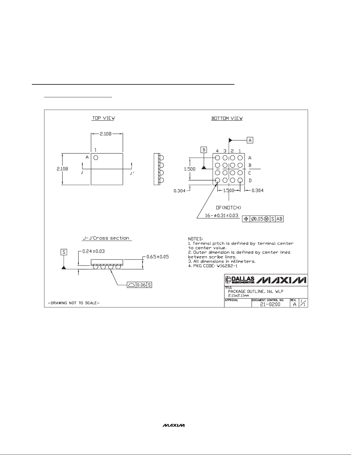
The MAX8805Y/MAX8805Z are available in a 16-bump,
2mm x 2mm WLP package (0.7mm max height).
Applications
WCDMA/NCDMA Cellular Handsets
Wireless PDAs
Smartphones
Features
♦ PA Step-Down Converter
7.5µs (typ) Settling Time for 0.8V to 3.4V Output
Voltage Change
Dynamic Output Voltage Setting from 0.4V to
V
BATT
60mΩ pFET and 100% Duty Cycle for Low
Dropout
2MHz or 4MHz Switching Frequency
Low Output-Voltage Ripple
600mA Output Drive Capability
2% Maximum Accuracy
Tiny External Components
♦ Dual Low-Noise LDOs
Low 35µV
RMS
(typ) Output Noise
High 70dB (typ) PSRR
Guaranteed 200mA Output Drive Capability
Individual ON/OFF Control
♦ Low 0.1µA Shutdown Current
♦ 2.7V to 5.5V Supply Voltage Range
♦ Thermal Shutdown
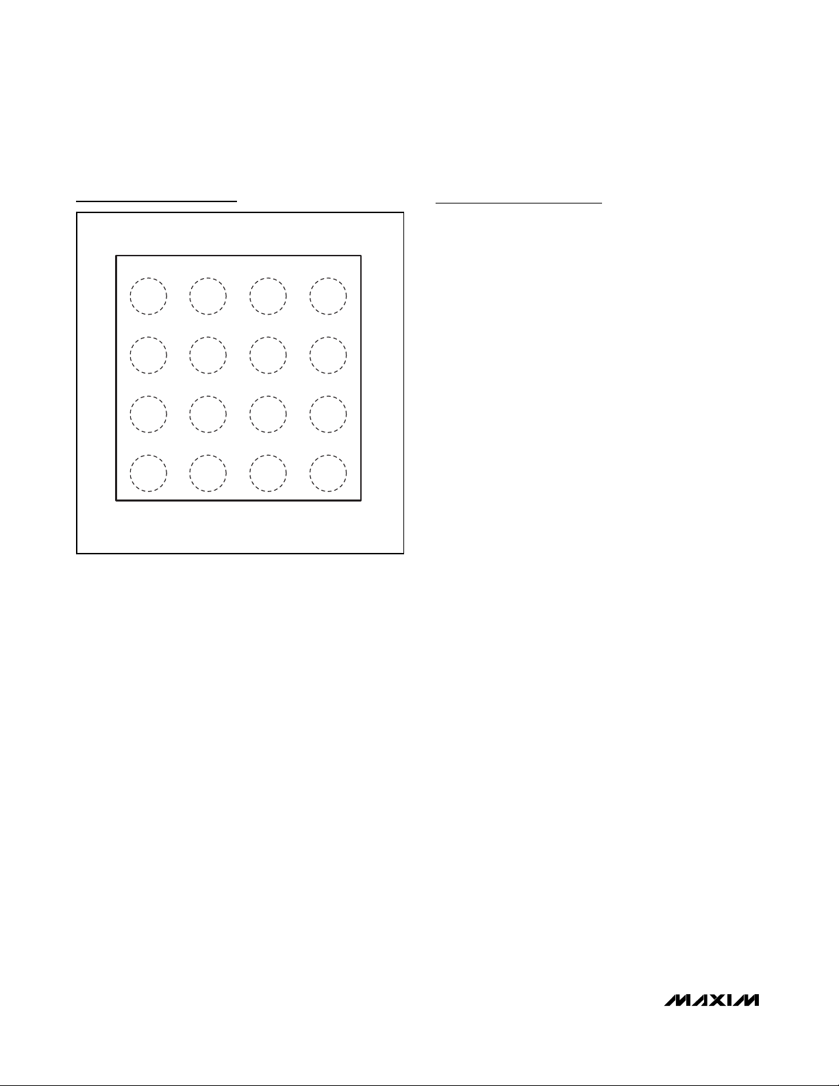
♦ Tiny 2mm x 2mm x 0.7mm WLP Package
(4 x 4 Grid)
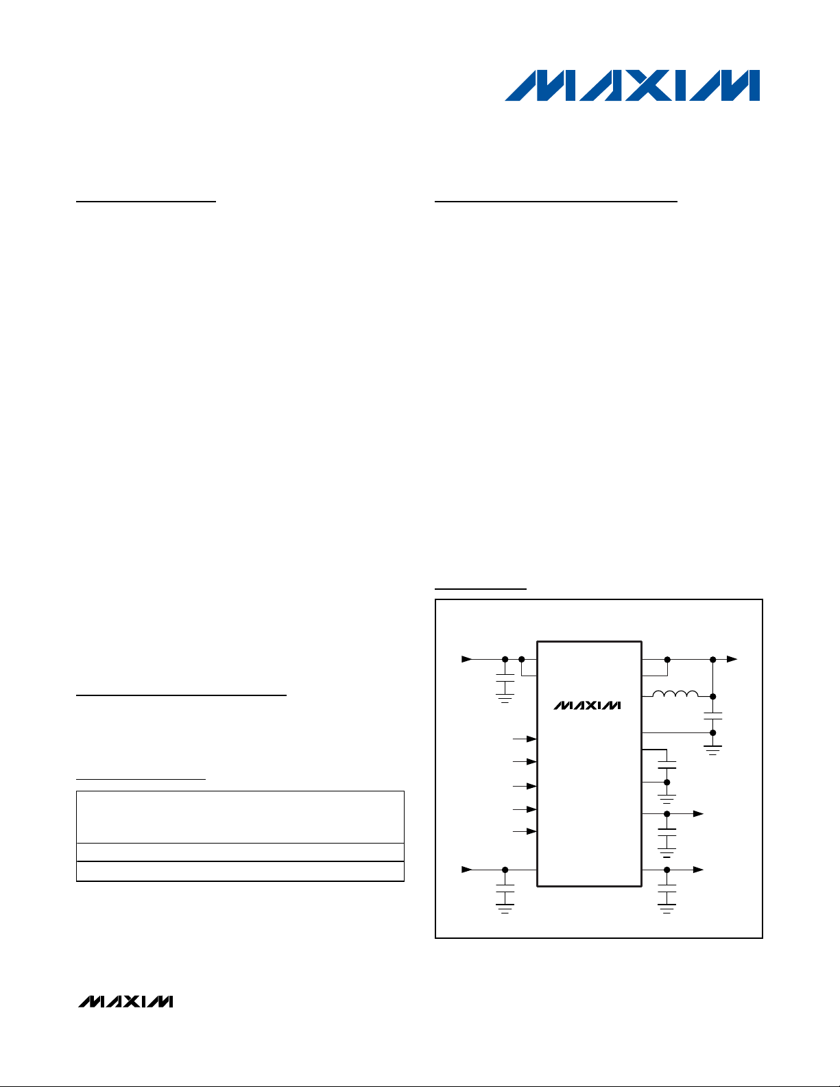
MAX8805Y/MAX8805Z
600mA PWM Step-Down Converters in
2mm x 2mm WLP for WCDMA PA Power
________________________________________________________________
Maxim Integrated Products
1
Ordering Information
IN1A
LX
PAA
1μH
BATT
2.7V TO 5.5V
AGND
PA_EN
REFIN
EN1
EN2
IN2
BATT
2.7V TO 5.5V
PA ON/OFF
ANALOG CONTROL
V
PA
0.4V TO V
BATT
REFBP
IN1B
LDO1 ON/OFF
LDO2 ON/OFF
PAB
LDO2
LDO1
V
LDO2
UP
TO 200mA
PGND
HP
FORCED BYPASS
2.2μF
2.2μF
MAX8805Z
V
LDO1
UP
TO 200mA
Typical Operating Circuit
19-0777; Rev 0; 4/07
For pricing, delivery, and ordering information, please contact Maxim/Dallas Direct! at
1-888-629-4642, or visit Maxim’s website at www.maxim-ic.com.
+
Denotes a lead-free package.
T
= Tape and reel package.
*
xy is the output voltage code (see Table 1 in the Output
Voltages section).
Note: All devices are specified over the -40°C to +85°C operating temperature range.
Pin Configuration appears at end of data sheet.
PART
PIN-
PKG
SWI T C H I N G
F R EQ U EN C Y
( M H z)
MAX8805YEWExy+T*
2
MAX8805ZEWExy+T*
4
PACKAGE
16 WLP-16 W162B2+ 1
16 WLP-16 W162B2+ 1
CODE
Page 2
MAX8805Y/MAX8805Z
600mA PWM Step-Down Converters in
2mm x 2mm WLP for WCDMA PA Power
2 _______________________________________________________________________________________
ABSOLUTE MAXIMUM RATINGS
ELECTRICAL CHARACTERISTICS
(V
IN1A
= V
IN1B
= V
IN2
= V
PA_EN
= V
EN1
= V
EN2
= 3.6V, V
HP
= 0V, V
REFIN
= 0.9V, TA= -40°C to +85°C. Typical values are at TA =
+25°C, unless otherwise noted.) (Note 1)
Stresses beyond those listed under “Absolute Maximum Ratings” may cause permanent damage to the device. These are stress ratings only, and functional
operation of the device at these or any other conditions beyond those indicated in the operational sections of the specifications is not implied. Exposure to
absolute maximum rating conditions for extended periods may affect device reliability.
IN1A, IN1B, IN2, REFIN, EN2, REFBP to AGND ...-0.3V to +6.0V
PAA, PAB, PA_EN, HP to AGND....-0.3V to (V
IN1A/VIN1B
+ 0.3V)
LDO1, LDO2, EN1 to AGND ......................-0.3V to (V
IN2
+ 0.3V)
IN2 to IN1B/IN1A ...................................................-0.3V to +0.3V
PGND to AGND .....................................................-0.3V to +0.3V
LX Current ......................................................................0.7A
RMS
IN1A/IN1B and PAA/PAB Current .....................................2A
RMS
PAA and PAB Short Circuit to GND or IN...................Continuous
Continuous Power Dissipation (T
A
= +70°C)
16-Bump WLP (derate 12.5mW/°C above +70°C).............1W
Junction Temperature......................................................+150°C
Storage Temperature Range .............................-65°C to +150°C
Bump Temperature (soldering, reflow) ............................+235°C
Note: This device is constructed using a unique set of packaging techniques that impose a limit on the thermal profile the device
can be exposed to during board level solder attach and rework. This limit permits only the use of the solder profiles recommended in the industry-standard specification, JEDEC 020A, paragraph 7.6, Table 3 for IR/VPR and Convection reflow.
Preheating is required. Hand or wave soldering is not allowed.
Dual Mode is a trademark of Maxim Integrated Products, Inc.
INPUT SUPPLY
Input Voltage V
Input Undervoltage Threshold V
Shutdown Supply Current V
No-Load Supply Current
THERMAL PROTECTION
Thermal Shutdown TA rising, 20°C typical hysteresis +160 °C
LOGIC CONTROL
PA_EN, EN1, EN2, HP LogicInput High Voltage
PA_EN, EN1, EN2, HP LogicInput Low Voltage
Logic-Input Current
(PA_EN, EN1, EN2, HP)
REFIN
REFIN Common-Mode Range 0.1 2.2 V
REFIN to PA_ Gain (Falling Edge) V
REFIN Input Resistance 540 kΩ
REFIN
Dual Mode™ Threshold
PARAMETER CONDITIONS MIN TYP MAX UNITS
, V
, V
= V
= 0V, I
= V
IN1B
IN1B
EN2
, V
IN2
, V
rising, 180mV typical hysteresis 2.52 2.63 2.70 V
IN2
= V
EN2
= I
= 0V
LDO2
EN1
LDO1
= 0V, IPA = 0A,
IN1A
IN1A
PA_EN
V
PA_EN
V
EN1
switching
V
= V
EN1
2.7V ≤ V
2.7V ≤ V
= 0V or V
V
IL
REFIN
V
REFIN
= 0V, VHP = 3.6V 150
EN2
IN1A
IN1A
= V
= V
IH
= V
IN1B
IN1B
IN1A
= V
= V
= 5.5V
= 0.4V, 0.9V, 1.7V, 2.2V 1.96 2.00 2.04 V/V
rising, 50mV hysteresis
2.7 5.5 V
TA = +25°C 0.1 4
T
= +85°C 0.1
A
= 0A 150 250
MAX8805Y 3500
MAX8805Z 5000
≤ 5.5V 1.4 V
IN2
≤ 5.5V 0.4 V
IN2
TA = +25°C 0.01 1
T
= +85°C 0.1
A
0.45 x
0.465 x
V
IN2
V
IN2
0.48 x
V
IN2
µA
µA
µA
V
Page 3
MAX8805Y/MAX8805Z
600mA PWM Step-Down Converters in
2mm x 2mm WLP for WCDMA PA Power
_______________________________________________________________________________________ 3
ELECTRICAL CHARACTERISTICS (continued)
(V
IN1A
= V
IN1B
= V
IN2
= V
PA_EN
= V
EN1
= V
EN2
= 3.6V, V
HP
= 0V, V
REFIN
= 0.9V, TA= -40°C to +85°C. Typical values are at TA =
+25°C, unless otherwise noted.) (Note 1)
LX
On-Resistance
LX Leakage Current
p-Channel MOSFET Peak
Current Limit
n-Channel MOSFET Valley
Current Limit
Minimum On- and Off-Times 0.1 µs
Power-Up Delay From PA_EN rising to LX rising 150 250 µs
BYPASS
On-Resistance
Bypass Current Limit VPA = 0 0.8 1.2 1.8 A
S tep - D ow n C ur r ent Li m i t i n Byp ass VLX = 0 0.7 0.9 1.1 A
Total Bypass Current Limit VLX = VPA = 0 1.5 2.1 2.9 A
Bypass Off-Leakage Current
LDO1
Output Voltage V
Output Current 200 mA
Current Limit V
Dropout Voltage I
Line Regulation V
Load Regulation I
Power-Supply Rejection
ΔV
LDO1
Output Noise 100Hz to 100kHz, C
Output Capacitor for Stable
Operation
Shutdown Output Impedance V
PARAMETER CONDITIONS MIN TYP MAX UNITS
p-channel MOSFET switch, ILX = -40mA 0.18 0.6
n-channel MOSFET rectifier, I
V
= V
IN1A
= 0V
V
LX
V
= 0V 0.7 0.9 1.1 A
LX
IN1B
= V
IN2
= 5.5V,
= 40mA 0.15 0.6
LX
TA = +25°C 0.1 5
T
= +85°C 1
A
0.5 0.7 0.9 A
p-channel MOSFET bypass,
= -90mA
I
OUT
V
V
IN1A
PAA
= V
= V
IN1B
PAB
= V
= 0V
IN2
= 5.5V,
TA = +25°C 0.060 0.1
T
= +85°C 0.1
A
TA = +25°C 0.01 10
T
= +85°C 1
A
MAX8805YEWEAA+T 1.746 1.8 1.854
MAX8805YEWEBC+T 2.425 2.5 2.575
LDO1
V
IN2
V
IN2
= 5.5V, I
= 3.4V, I
LDO1
LDO1
= 1mA;
= 100mA
MAX8805YEWECC+T 2.619 2.7 2.781
MAX8805YEWEDD+T 2.716 2.8 2.884
MAX8805YEWEEE+T 2.765 2.85 2.936
/ ΔV
IN2
MAX8805YEWEGG+T 2.910 3.0
= 0V 250 550 750 mA
LDO1
= 100mA, TA = +25°C (V
LDO1
stepped from 3.5V to 5.5V, I
IN2
stepped from 50µA to 200mA 25 mV
LDO1
10Hz to 10kHz, C
0 < I
0 < I
EN1
< 10mA 100 nF
LDO1
< 200mA 1 µF
LDO1
= 0V 1 kΩ
LDO1
LDO1
= 1µF, I
= 1µF, I
≥ 2.5V) 70 200 mV
LDO1
= 100mA 2.4 mV
LDO1
= 30mA 70 dB
LDO1
= 30mA 35 µV
LDO1
3.090
Ω
µA
Ω
µA
V
RMS
Page 4
MAX8805Y/MAX8805Z
600mA PWM Step-Down Converters in
2mm x 2mm WLP for WCDMA PA Power
4 _______________________________________________________________________________________
ELECTRICAL CHARACTERISTICS (continued)
(V
IN1A
= V
IN1B
= V
IN2
= V
PA_EN
= V
EN1
= V
EN2
= 3.6V, V
HP
= 0V, V
REFIN
= 0.9V, TA= -40°C to +85°C. Typical values are at TA =
+25°C, unless otherwise noted.) (Note 1)
Note 1: All devices are 100% production tested at TA= +25°C. Limits over the operating temperature range are guaranteed by design.
LDO2
Output Voltage V
Output Current 200 mA
Current Limit V
Dropout Voltage I
Line Regulation V
Load Regulation I
Power-Supply Rejection
ΔV
LDO2
Output Noise 100Hz to 100kHz, C
Output Capacitor for Stable
Operation
Shutdown Output Impedance V
REFBP
REFBP Output Voltage 0 ≤ I
REFBP Supply Rejection V
PARAMETER CONDITIONS MIN TYP MAX UNITS
/ ΔV
IN2
LDO2
V
= 5.5V, I
IN2
V
= 3.4V, I
IN2
= 0V 250 550 750 mA
LDO2
= 100mA, TA = +25°C 70 200 mV
LDO2
stepped from 3.5V to 5.5V, I
IN2
stepped from 50µA to 200mA 25 mV
LDO2
10Hz to 10kHz, C
0µA < I
0µA < I
= 0V 1 kΩ
EN2
REFBP
stepped from 2.55V to 5.5V 0.2 5 mV
IN2
LDO2
LDO2
< 10mA 100 nF
LDO2
< 200mA 1 µF
LDO2
≤ 1µA 1.237 1.250 1.263 V
= 1mA;
= 100mA
= 1µF, I
LDO2
LDO2
= 1µF, I
MAX8805YEWEAA+T 1.746 1.8 1.854
MAX8805YEWEAC+T 2.619 2.7 2.781
MAX8805YEWEAD+T 2.716 2.8 2.884
MAX8805YEWEBE+T 2.765 2.85 2.936
MAX8805YEWEGG+T 2.910 3.0
= 100mA 2.4 mV
LDO2
= 30mA 70 dB
LDO2
= 30mA 35 µV
LDO2
V
3.090
RMS
Page 5
MAX8805Y/MAX8805Z
600mA PWM Step-Down Converters in
2mm x 2mm WLP for WCDMA PA Power
_______________________________________________________________________________________
5
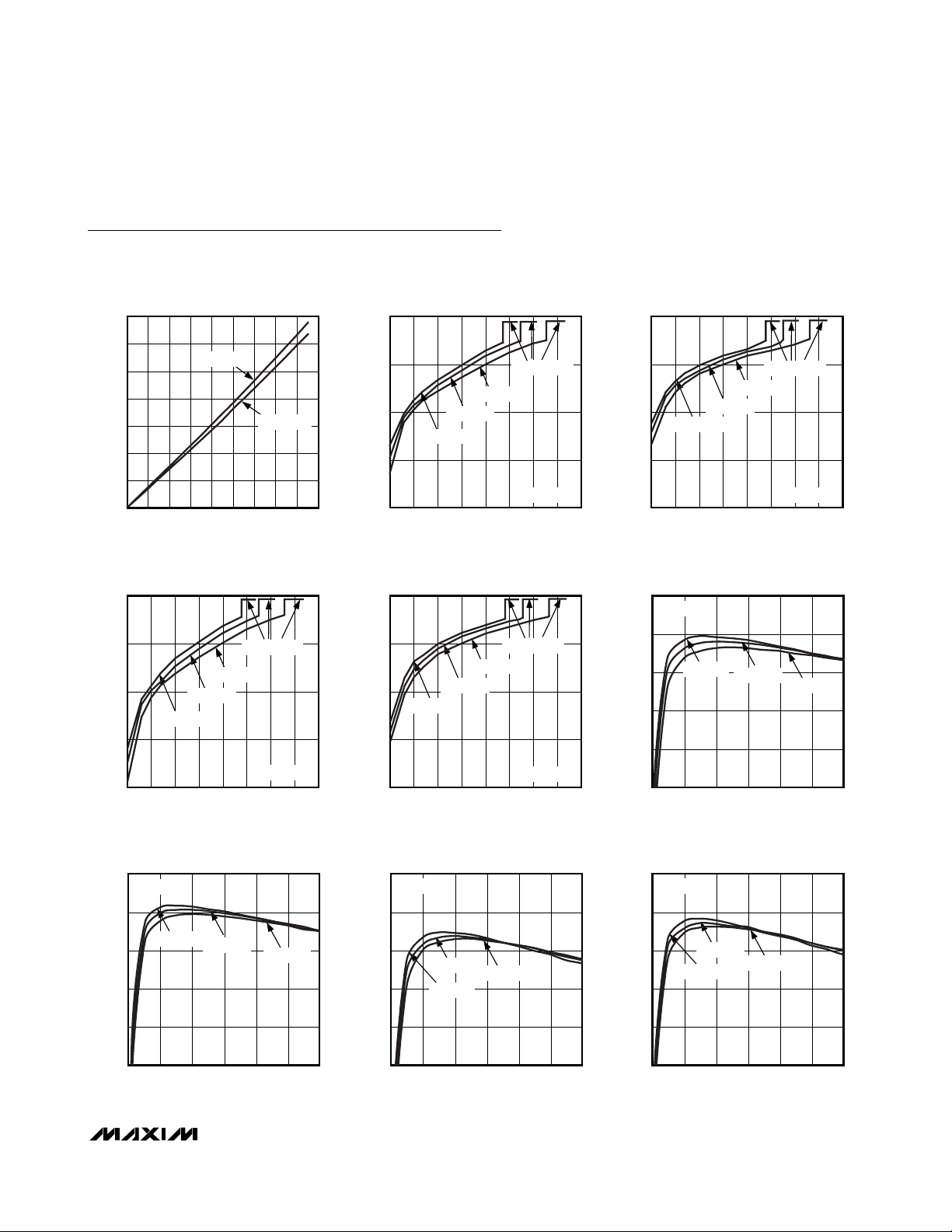
Typical Operating Characteristics
(V
IN1A
= V
IN1B
= V
IN2
= 3.6V, VPA= 1.2V, V
LDO1
= 2.85V, V
LDO2
= 2.85V, RPA= 7.5Ω, circuit of Figure 5, TA= +25°C, unless other-
wise noted.)
0
40
20
80
60
120
100
140
0 0.4 0.60.2 0.8 1.0 1.2 1.4 1.6 1.8
BYPASS MODE DROPOUT VOLTAGE
vs. PA LOAD CURRENT
MAX8805Y/Z toc01
PA LOAD CURRENT (A)
BYPASS MODE DROPOUT VOLTAGE (mV)
V
IN1
= 3.2V
V
IN1
= 3.6V
60
70
80
90
100
0.5 1.5 2.5 3.51.0 2.0 3.0 4.0 4.5
PA STEP-DOWN CONVERTER EFFICIENCY
vs. OUTPUT VOLTAGE (MAX8805Z)
MAX8805Y/Z toc02
OUTPUT VOLTAGE (V)
EFFICIENCY (%)
BYPASS MODE
V
IN1
= 4.2V
V
IN1
= 3.6V
V
IN1
= 3.2V
RPA = 7.5Ω
60
70
80
90
100
0.5 1.5 2.5 3.51.0 2.0 3.0 4.0 4.5
PA STEP-DOWN CONVERTER EFFICIENCY
vs. OUTPUT VOLTAGE (MAX8805Y)
MAX8805Y/Z toc03
OUTPUT VOLTAGE (V)
EFFICIENCY (%)
BYPASS MODE
V
IN1
= 4.2V
V
IN1
= 3.6V
V
IN1
= 3.2V
RPA = 7.5Ω
60
70
80
90
100
0.5 1.5 2.5 3.51.0 2.0 3.0 4.0 4.5
PA STEP-DOWN CONVERTER EFFICIENCY
vs. OUTPUT VOLTAGE (MAX8805Z)
MAX8805Y/Z toc04
OUTPUT VOLTAGE (V)
EFFICIENCY (%)
BYPASS MODE
V
IN1
= 4.2V
V
IN1
= 3.6V
V
IN1
= 3.2V
RPA = 10Ω
60
70
80
90
100
0.5 1.5 2.5 3.51.0 2.0 3.0 4.0 4.5
PA STEP-DOWN CONVERTER EFFICIENCY
vs. OUTPUT VOLTAGE (MAX8805Y)
MAX8805Y/Z toc05
OUTPUT VOLTAGE (V)
EFFICIENCY (%)
BYPASS MODE
V
IN1
= 4.2V
V
IN1
= 3.6V
V
IN1
= 3.2V
RPA = 10Ω
50
60
80
70
90
100
0200100 300 400 500 600
PA STEP-DOWN CONVERTER EFFICIENCY
vs. LOAD CURRENT (MAX8805Z)
MAX8805Y/Z toc06
LOAD CURRENT (mA)
EFFICIENCY (%)
V
IN1
= 4.2V
V
IN1
= 3.6V
V
IN1
= 3.2V
VPA = 1.8V
50
60
80
70
90
100
0 200100 300 500400 600
PA STEP-DOWN CONVERTER EFFICIENCY
vs. LOAD CURRENT (MAX8805Y)
MAX8805Y/Z toc07
LOAD CURRENT (mA)
EFFICIENCY (%)
V
IN1
= 4.2V
V
IN1
= 3.6V
V
IN1
= 3.2V
VPA = 1.8V
50
60
80
70
90
100
0200100 300 500400 600
PA STEP-DOWN CONVERTER EFFICIENCY
vs. LOAD CURRENT (MAX8805Z)
MAX8805Y/Z toc08
LOAD CURRENT (mA)
EFFICIENCY (%)
V
IN1
= 4.2V
V
IN1
= 3.6V
V
IN1
= 3.2V
VPA = 1.2V
50
60
80
70
90
100
0200100 300 500400 600
PA STEP-DOWN CONVERTER EFFICIENCY
vs. LOAD CURRENT (MAX8805Y)
MAX8805Y/Z toc09
LOAD CURRENT (mA)
EFFICIENCY (%)
V
IN1
= 4.2V
V
IN1
= 3.6V
V
IN1
= 3.2V
VPA = 1.2V
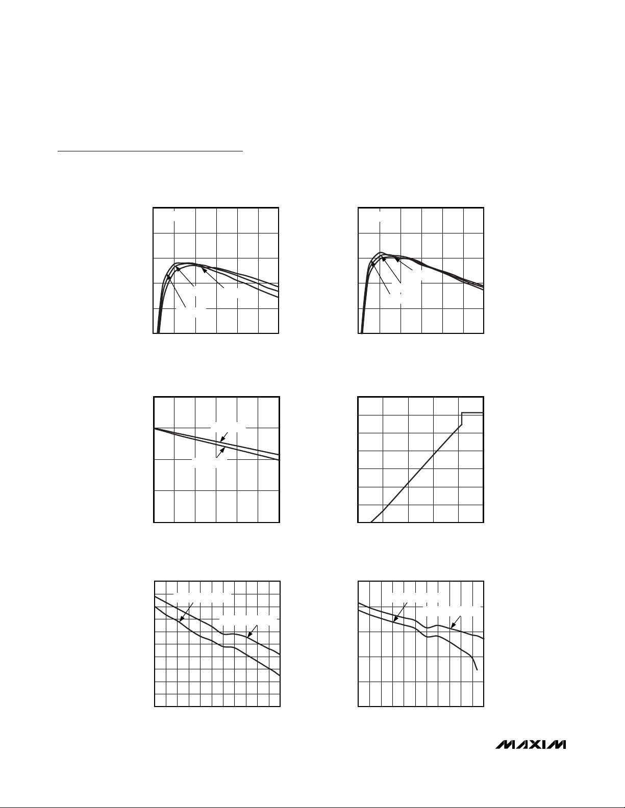
Page 6
MAX8805Y/MAX8805Z
600mA PWM Step-Down Converters in
2mm x 2mm WLP for WCDMA PA Power
6 _______________________________________________________________________________________
Typical Operating Characteristics (continued)
(V
IN1A
= V
IN1B
= V
IN2
= 3.6V, VPA= 1.2V, V
LDO1
= 2.85V, V
LDO2
= 2.85V, RPA= 7.5Ω, circuit of Figure 5, TA= +25°C, unless other-
wise noted.)
50
60
80
70
90
100
0 200100 300 500400 600
PA STEP-DOWN CONVERTER EFFICIENCY
vs. LOAD CURRENT (MAX8805Z)
MAX8805Y/Z toc10
LOAD CURRENT (mA)
EFFICIENCY (%)
V
IN1
= 4.2V
V
IN1
= 3.6V
V
IN1
= 3.2V
VPA = 0.6V
50
60
80
70
90
100
0 200100 300 500400 600
PA STEP-DOWN CONVERTER EFFICIENCY
vs. LOAD CURRENT (MAX8805Y)
MAX8805Y/Z toc11
LOAD CURRENT (mA)
EFFICIENCY (%)
V
IN1
= 4.2V
V
IN1
= 3.6V
V
IN1
= 3.2V
VPA = 0.6V
1.25
1.20
1.15
1.10
1.05
0 300100 200 400 500 600
PA STEP-DOWN CONVERTER OUTPUT
VOLTAGE vs. LOAD CURRENT
MAX8805Y/Z toc12
LOAD CURRENT (mA)
OUTPUT VOLTAGE (V)
MAX8805Y
MAX8805Z
0.5
1.5
1.0
2.5
2.0
3.5
3.0
4.0
00.80.4 1.2 1.6 2.0
PA STEP-DOWN CONVERTER OUTPUT
VOLTAGE vs. REFIN VOLTAGE
MAX8805Y/Z toc13
REFIN VOLTAGE (V)
OUTPUT VOLTAGE (V)
-100
-60
-80
0
-20
-40
20
40
80
60
100
0.4 0.6 0.70.5 0.8 0.9 1.0 1.1 1.2 1.3 1.4 1.5
REFIN vs. REFIN TO OUT GAIN (MAX8805Z)
MAX8805Y/Z toc14
REFIN VOLTAGE (V)
OUTPUT VOLTAGE ERROR (mV)
V
IN1
= 3.2V, NO LOAD
V
IN1
= 4.2V, NO LOAD
-50
-30
-10
10
30
50
0.4 0.6 0.70.5 0.8 0.9 1.0 1.1 1.2 1.3 1.4 1.5
REFIN vs. REFIN TO OUT GAIN (MAX8805Y)
MAX8805Y/Z toc15
REFIN VOLTAGE (V)
OUTPUT VOLTAGE ERROR (mV)
V
IN1
= 3.2V, NO LOAD
V
IN1
= 4.2V, NO LOAD
Page 7
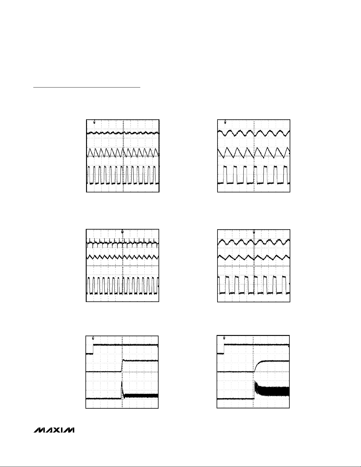
400ns/div
PA STEP-DOWN CONVERTER LIGHT-LOAD
SWITCHING WAVEFORMS (MAX8805Z)
V
PA
AC-COUPLED
I
LX
200mA/div
20mV/div
2V/div
MAX8805Y/Z toc16
V
LX
VPA = 1.2V, IPA = 50mA
400ns/div
PA STEP-DOWN CONVERTER LIGHT-LOAD
SWITCHING WAVEFORMS (MAX8805Y)
V
PA
AC-COUPLED
I
LX
200mA/div
20mV/div
2V/div
MAX8805Y/Z toc17
V
LX
VPA = 1.2V, IPA = 50mA
400ns/div
PA STEP-DOWN HEAVY-LOAD
SWITCHING WAVEFORMS (MAX8805Z)
V
PA
AC-COUPLED
I
LX
500mA/div
20mV/div
2V/div
MAX8805Y/Z toc18
V
LX
VPA = 1.2V, IPA = 500mA
MAX8805Y/MAX8805Z
600mA PWM Step-Down Converters in
2mm x 2mm WLP for WCDMA PA Power
_______________________________________________________________________________________
7
Typical Operating Characteristics (continued)
(V
IN1A
= V
IN1B
= V
IN2
= 3.6V, VPA= 1.2V, V
LDO1
= 2.85V, V
LDO2
= 2.85V, RPA= 7.5Ω, circuit of Figure 5, TA= +25°C, unless other-
wise noted.)
_______________________________________________________________________________________
7
PA STEP-DOWN HEAVY-LOAD
V
AC-COUPLED
SWITCHING WAVEFORMS (MAX8805Y)
PA
MAX8805Y/Z toc19
20mV/div
V
PA_EN
V
PA
I
LX
PA STEP-DOWN SOFT-START
WAVEFORMS (MAX8805Z)
20μs/div
MAX8805Y/Z toc20
2V/div
1V/div
500mA/div
V
PA_EN
V
I
LX
V
LX
PA STEP-DOWN SOFT-START
WAVEFORMS (MAX8805Y)
PA
I
LX
500mA/div
2V/div
VPA = 1.2V, IPA = 500mA
400ns/div
MAX8805Y/Z toc21
2V/div
1V/div
200mA/div
20μs/div
Page 8

MAX8805Y/MAX8805Z
600mA PWM Step-Down Converters in
2mm x 2mm WLP for WCDMA PA Power
8 _______________________________________________________________________________________
Typical Operating Characteristics (continued)
(V
IN1A
= V
IN1B
= V
IN2
= 3.6V, VPA= 1.2V, V
LDO1
= 2.85V, V
LDO2
= 2.85V, RPA= 7.5Ω, circuit of Figure 5, TA= +25°C, unless other-
wise noted.)
10μs/div
PA STEP-DOWN CONVERTER OUTPUT
VOLTAGE TRANSIENT RESPONSE
V
REFIN
V
PA
500mV/div
500mV/div
500mA/div
MAX8805Y/Z toc26
I
LX
0.5V
1V
0.5V
20μs/div
PA STEP-DOWN CONVERTER FORCED
BYPASS-FET TRANSIENT RESPONSE
V
HP
V
PA
2V/div
2V/div
500mA/div
MAX8805Y/Z toc27
I
LX
0.5V
0V
0V
1.2V
1.2V
3.6V
10μs/div
PA STEP-DOWN CONVERTER LOAD
TRANSIENT RESPONSE (MAX8805Y)
I
PA
I
LX
500mA/div
500mA/div
100mV/div
MAX8805Y/Z toc25
V
PA
AC-COUPLED
0mA
500mA
0mA
10μs/div
PA STEP-DOWN CONVERTER LOAD
TRANSIENT RESPONSE (MAX8805Z)
I
PA
I
LX
500mA/div
500mA/div
100mV/div
MAX8805Y/Z toc24
V
PA
AC-COUPLED
0mA
500mA
0mA
10μs/div
PA STEP-DOWN CONVERTER LINE
TRANSIENT RESPONSE (MAX8805Z)
V
IN1
V
PA
AC-COUPLED
50mV/div
500mV/div
200mA/div
MAX8805Y/Z toc22
I
LX
4.0V
3.5V
4.0V
10μs/div
PA STEP-DOWN CONVERTER LINE
TRANSIENT RESPONSE (MAX8805Y)
V
IN1
V
PA
AC-COUPLED
50mV/div
500mV/div
200mA/div
MAX8805Y/Z toc23
I
LX
4.0V
3.5V
4.0V
Page 9

MAX8805Y/MAX8805Z
600mA PWM Step-Down Converters in
2mm x 2mm WLP for WCDMA PA Power
_______________________________________________________________________________________
9
Typical Operating Characteristics (continued)
(V
IN1A
= V
IN1B
= V
IN2
= 3.6V, VPA= 1.2V, V
LDO1
= 2.85V, V
LDO2
= 2.85V, RPA= 7.5Ω, circuit of Figure 5, TA= +25°C, unless other-
wise noted.)
PA STEP-DOWN CONVERTER AUTOMATIC
BYPASS-FET TRANSIENT RESPONSE
1.8V
V
REFIN
0.6V
3.6V
V
PA
1.2V
I
LX
10μs/div
PA STEP-DOWN CONVERTER
SHUTDOWN RESPONSE (MAX8805Y)
2V
V
PA_EN
V
1.2V
PA
0V
MAX8805Y/Z toc28
MAX8805Y/Z toc30
0.6V
1.2V
1V/div
2V/div
500mA/div
2V/div
1V/div
PA STEP-DOWN CONVERTER AUTOMATIC
BYPASS-FET TRANSIENT RESPONSE
V
IS A 0.4V TO
REFIN
2V SINUSOIDAL
V
SIGNAL
REFIN
V
PA
I
LX
3.6V
200μs/div
MAX8805Y/Z toc29
1V/div
1V/div
500mA/div
PA STEP-DOWN CONVERTER
SHUTDOWN RESPONSE (MAX8805Z)
2V
V
PA_EN
1.2V
V
PA
0V
MAX8805Y/Z toc31
2V/div
2V/div
I
LX
10μs/div
LDO1, LDO2 SUPPLY CURRENT
vs. SUPPLY VOLTAGE
200
150
100
50
NO-LOAD SUPPLY CURRENT (μA)
0
2.0 3.5 4.02.5 3.0 4.5 5.0 5.5
SUPPLY VOLTAGE (V)
100mA/div
MAX8805Y/Z toc32
I
LX
10μs/div
LDO1, LDO2 DROPOUT VOLTAGE
vs. LOAD CURRENT
150
120
90
60
30
LDO1, LDO2 DROPOUT VOLTAGE (mV)
0
0 10050 150 200
LOAD CURRENT (mA)
100mA/div
MAX8805Y/Z toc33
Page 10

MAX8805Y/MAX8805Z
600mA PWM Step-Down Converters in
2mm x 2mm WLP for WCDMA PA Power
10 ______________________________________________________________________________________
Typical Operating Characteristics (continued)
(V
IN1A
= V
IN1B
= V
IN2
= 3.6V, VPA= 1.2V, V
LDO1
= 2.85V, V
LDO2
= 2.85V, RPA= 7.5Ω, circuit of Figure 5, TA= +25°C, unless other-
wise noted.)
80
70
60
50
PSRR (dB)
40
30
LDO PSRR vs. FREQUENCY
MAX8805Y/Z toc34
LDO OUTPUT NOISE SPECTRAL DENSITY
vs. FREQUENCY
1.0E+04
1.0E+03
1.0E+02
MAX8805Y/Z toc35
20
I
= 30mA
LDO
10
0.01 1000
FREQUENCY (kHz)
LDO1, LDO2 OUTPUT NOISE WAVEFORM
400μs/div
1001010.1
MAX8805Y/Z toc36
50mV/div
LDO1, LDO2 LOAD TRANSIENT
I
LDO1
RESPONSE NEAR DROPOUT
80mA
0mA
MAX8805Y/Z toc38
0mA
100mA/div
OUTPUT NOISE DENSITY NOISE (nV/√Hz)
1.0E+01
0.01 1000
FREQUENCY (kHz)
LDO LINE TRANSIENT RESPONSE
4.0V
V
V
IN2
LDO_
3.5V
20μs/div
LDO1, LDO2 TURN ON AND
SHUTDOWN RESPONSE
V
EN1,2
1001010.1
MAX8805Y/Z toc37
I
LDO_
MAX8805Y/Z toc39
4.0V
500mV/div
5mV/div
= 80mA
2V/div
V
V
LDO1
I
LDO2
LDO2
0mA
80mA
V
IN2
20μs/div
= V
LDO1,2
0mA
+ 200mV
50mV/div
100mA/div
50mV/div
V
LDO1
V
LDO2
1ms/div
2V/div
2V/div
Page 11

MAX8805Y/MAX8805Z
600mA PWM Step-Down Converters in
2mm x 2mm WLP for WCDMA PA Power
______________________________________________________________________________________ 11
Pin Description
PIN NAME FUNCTION
A1 REFBP
A2 AGND Low-Noise Analog Ground
A3 REFIN
A4 PGND Power Ground for PA Step-Down Converter
B1 LDO2
B2 PA_EN
B3 EN2
B4 LX Inductor Connection. Connect an inductor from LX to the output of the PA step-down converter.
C1 IN2
C2 HP
C3, C4
D1 LDO1
D2 EN1
D3, D4 PAB, PAA
IN1B,
IN1A
Reference Noise Bypass. Bypass REFBP to AGND with a 0.22µF ceramic capacitor to reduce noise on the
LDO outputs. REFBP is internally pulled down through a 1kΩ resistor during shutdown.
DAC-Controlled Input. The output of the PA step-down converter is regulated to 2 x V
reaches 0.465 x V
200mA LDO Regulator 2 Output. Bypass LDO2 with a 1µF ceramic capacitor as close as possible to LDO2
and AGND. LDO2 is internally pulled down through a 1kΩ resistor when this regulator is disabled.
PA Step-Down Converter Enable Input. Connect to IN_ or logic-high for normal operation. Connect to GND
or logic-low for shutdown mode.
LDO2 Enable Input. Connect to IN2 or logic-high for normal operation. Connect to AGND or logic-low for
shutdown mode.
Supply Voltage Input for LDO1, LDO2, and Internal Reference. Connect IN2 to a battery or supply voltage
from 2.7V to 5.5V. Bypass IN2 with a 2.2µF ceramic capacitor as close as possible to IN2 and AGND.
Connect IN2 to the same source as IN1A and IN1B.
High-Power Mode Set Input. Drive HP high to invoke forced bypass mode. Bypass mode connects the
input of the PA step-down converter directly to its output through the internal bypass MOSFET. Drive HP
low to disable the forced bypass mode.
Supply Voltage Input for PA Step-Down Converter. Connect IN1_ to a battery or supply voltage from 2.7V to
5.5V. Bypass the connection of IN1_ with a 2.2µF ceramic capacitor as close as possible to IN1_, and
PGND. IN1A
200mA LDO Regulator 1 Output. Bypass LDO1 with a 1µF ceramic capacitor as close as possible to LDO1
and AGND. LDO1 is internally pulled down through a 1kΩ resistor when this regulator is disabled.
LDO1 Enable Input. Connect to IN2 or logic-high for normal operation. Connect to AGND or logic-low for
shutdown mode.
PA Connection for Bypass Mode. Internally connected to IN1_ using the internal bypass MOSFET during
bypass mode. PA_ is connected to the internal feedback network. Bypass PA_ with a 2.2µF ceramic
capacitor as close as possible to PA_ and PGND.
and IN1B are internally connected together. Connect IN1_ to the same source as IN2.
, bypass mode is enabled.
IN2
REFIN
. When V
REFIN
Page 12

MAX8805Y/MAX8805Z
600mA PWM Step-Down Converters in
2mm x 2mm WLP for WCDMA PA Power
12 ______________________________________________________________________________________
Figure 1. Block Diagram
IN1A
IN1B
R5R4
BYPASS FET
PAA
HP
PWM ERROR
REFIN
R7
C2
R6
IN2
REFBP
AGND
EN1
EN2
PA_EN
1.25V
REFERENCE
BANDGAP
CONTROL
LOGIC
COMPARATOR
R2 R1
BANDGAP
BANDGAP
CURRENT-LIMIT CONTROL
PWM LOGIC
STEP-DOWN CURRENT LIMIT
ERROR AMP
C1
LDO1 CURRENT LIMIT
LDO2 CURRENT LIMIT
R3
R9
R8
R7
PAB
LX
PGND
LDO1
ERROR AMP
R12
LDO2
R11
R10
Page 13

MAX8805Y/MAX8805Z
600mA PWM Step-Down Converters in
2mm x 2mm WLP for WCDMA PA Power
______________________________________________________________________________________ 13
Detailed Description
The MAX8805Y/MAX8805Z are designed to dynamically power the PA in WCDMA and NCDMA handsets. The
devices contain a high-frequency, high-efficiency stepdown converter, and two LDOs. The step-down converter delivers over 600mA. The hysteretic PWM control
scheme provides extremely fast transient response,
while 2MHz and 4MHz switching-frequency options
allow the trade-off between efficiency and the smallest
external components. A 60mΩ bypass FET connects
the PA directly to the battery during high-power transmission.
Step-Down Converter Control Scheme
A hysteretic PWM control scheme ensures high efficiency, fast switching, fast transient response, low-output ripple, and physically tiny external components.
The control scheme is simple: when the output voltage
is below the regulation threshold, the error comparator
begins a switching cycle by turning on the high-side
switch. This high-side switch remains on until the minimum on-time expires and the output voltage is within
regulation, or the inductor current is above the currentlimit threshold. Once off, the high-side switch remains
off until the minimum off-time expires and the output
voltage falls again below the regulation threshold.
During the off period, the low-side synchronous rectifier
turns on and remains on until the high-side switch turns
on again. The internal synchronous rectifier eliminates
the need for an external Schottky diode.
Voltage-Positioning Load Regulation
The MAX8805Y/MAX8805Z step-down converters utilize
a unique feedback network. By taking DC feedback
from the LX node through R1 in Figure 1, the usual
phase lag due to the output capacitor is removed, making the loop exceedingly stable and allowing the use of
very small ceramic output capacitors. To improve the
load regulation, resistor R3 is included in the feedback.
This configuration yields load regulation equal to half of
the inductor’s series resistance multiplied by the load
current. This voltage-positioning load regulation greatly
reduces overshoot during load transients or when
changing the output voltage from one level to another.
However, when calculating the required REFIN voltage,
the load regulation should be considered. Because
inductor resistance is typically well specified and the
typical PA is a resistive load, the MAX8805Y/MAX8805Z
V
REFIN
to V
OUT
gain is slightly less than 2V/V.
Step-Down Converter Bypass Mode
During high-power transmission, the bypass mode connects IN1A and IN1B directly to PAA and PAB with the
internal 60mΩ (typ) bypass FET, while the step-down
converter is forced into 100% duty-cycle operation. The
low on-resistance in this mode provides low dropout,
long battery life, and high output current capability.
Forced and Automatic Bypass Mode
Invoke forced bypass mode by driving HP high or
invoke automatic bypass mode by applying a high voltage to REFIN. To prevent excessive output ripple as the
step-down converter approaches dropout, the
MAX8805Y/MAX8805Z enter bypass mode automatically
when V
REFIN
> 0.465 x V
IN2
(see Figure 2). Note that
IN2 is used instead of IN1 to prevent switching noise
from causing false enagement of automatic bypass
mode. For this reason, IN2 must be connected to the
same source as IN1.
Shutdown Mode
Connect PA_EN to GND or logic-low to place the
MAX8805Y/MAX8805Z PA step-down converter in shutdown mode. In shutdown, the control circuitry, internal
switching MOSFET, and synchronous rectifier turn off
and LX becomes high impedance. Connect PA_EN to
IN1_ or logic-high for normal operation.
Connect EN1 or EN2 to GND or logic-low to place
LDO1 or LDO2, respectively, in shutdown mode. In
shutdown, the outputs of the LDOs are pulled to ground
through an internal 1kΩ resistor.
When the PA step-down and LDOs are all in shutdown,
the MAX8805Y/MAX8805Z enter a very low power
state, where the input current drops to 0.1µA (typ).
Figure 2. V
IN2
and V
PA_
with Automatic Entry/Exit into Bypass
Mode
2.5
2.0
1.5
1.0
REFIN VOLTAGE (V)
0.5
0
IN2 AND PA_
5.0
4.5
4.0
3.5
3.0
2.5
VOLTAGE (V)
2.0
1.5
1.0
0.5
0
IN2
PA_
REFIN
010152052530354540 50
TIME (ms)
Page 14

MAX8805Y/MAX8805Z
600mA PWM Step-Down Converters in
2mm x 2mm WLP for WCDMA PA Power
14 ______________________________________________________________________________________
Step-Down Converter Soft-Start
The MAX8805Y/MAX8805Z PA step-down converter has
internal soft-start circuitry that limits inrush current at
startup, reducing transients on the input source. Softstart is particularly useful for supplies with high output
impedance such as Li+ and alkaline cells. See the SoftStart Waveforms in the
Typical Operating Characteristics.
Analog REFIN Control
The MAX8805Y/MAX8805Z PA step-down converter uses
REFIN to set the output voltage. The output voltage is regulated at twice the voltage applied at REFIN minus the
load regulation. This allows the converter to operate in
applications where dynamic voltage control is required.
Thermal Shutdown
Thermal shutdown limits total power dissipation in the
MAX8805Y/MAX8805Z. If the junction temperature
exceeds +160°C, thermal-shutdown circuitry turns off
the IC, allowing it to cool. The IC turns on and begins
soft-start after the junction temperature cools by 20°C.
This results in a pulsed output during continuous thermal-overload conditions.
Applications Information
Output Voltages
The MAX8805Y/MAX8805Z PA step-down converters
set the PA_ output voltage to twice the voltage applied
to REFIN.
LDO1 and LDO2 output voltages are determined by the
part number suffix, as shown in Table 1.
LDO Dropout Voltage
The regulator’s minimum input/output differential (or
dropout voltage) determines the lowest usable supply
voltage. In battery-powered systems, this determines
the useful end-of-life battery voltage. Because the
MAX8805Y/MAX8805Z LDOs use a p-channel MOSFET
pass transistor, their dropout voltages are a function of
drain-to-source on-resistance (R
DS
(ON)) multiplied by the
load current (see the
Typical Operating Characteristics
).
Inductor Selection
The MAX8805Y operates with a switching frequency of
2MHz and utilizes a 2.2µH inductor. The MAX8805Z
operates with a switching frequency of 4MHz and utilizes a 1µH inductor. The higher switching frequency of
the MAX8805Z allows the use of physically smaller
inductors at the cost of slightly lower efficiency. The
lower switching frequency of the MAX8805Y results in
greater efficiency at the cost of a physically larger
inductor. See the
Typical Operating Characteristics
for
efficiency graphs for both the MAX8805Y and
MAX8805Z.
The inductor’s DC current rating only needs to match the
maximum load of the application because the
MAX8805Y/MAX8805Z feature zero current overshoot
during startup and load transients. For optimum transient
response and high efficiency, choose an inductor with
DC series resistance in the 50mΩ to 150mΩ range. See
Table 2 for suggested inductors and manufacturers.
Output Capacitor Selection
For the PA step-down converter, the output capacitor
(CPA) is required to keep the output voltage ripple small
and ensure regulation loop stability. CPAmust have low
impedance at the switching frequency. Ceramic capacitors with X5R or X7R dielectric are highly recommended
due to their small size, low ESR, and small temperature
coefficients. Due to the unique feedback network, the
output capacitance can be very low. A 2.2µF capacitor
is recommended for most applications. For optimum
load-transient performance and very low output ripple,
the output capacitor value can be increased.
For LDO1 and LDO2, the minimum output capacitance
required is dependent on the load currents. For loads
less than 10mA, it is sufficient to use a 0.1µF capacitor
for stable operation over the full temperature range.
With rated maximum load currents, a minimum of 1µF is
recommended. Reduce output noise and improve loadtransient response, stability, and power-supply rejection by using larger output capacitors.
Note that some ceramic dielectrics exhibit large capacitance and ESR variation with temperature. With dielectrics
such as Z5U and Y5V, it is necessary to use 2.2µF or larger to ensure stability at temperatures below -10°C. With
X7R or X5R dielectrics, 1µF is sufficient at all operating
temperatures. These regulators are optimized for ceramic
capacitors. Tantalum capacitors are not recommended.
Table 1. LDO1 and LDO2 Output Voltage
Selection
Note: Contact the factory for other output-voltage options.
PART
FREQUENCY
(MHz)
LDO1
(V)
LDO2
(V)
2 1.80 1.80
2 1.80 2.85
2 2.85 2.85
4 1.80 1.80
4 1.80 2.85
4 2.85 2.85
MAX8805YEWEAA+T
MAX8805YEWEAE+T
MAX8805YEWEEE+T
MAX8805ZEWEAA+T
MAX8805ZEWEAE+T
MAX8805ZEWEEE+T
Page 15

MAX8805Y/MAX8805Z
600mA PWM Step-Down Converters in
2mm x 2mm WLP for WCDMA PA Power
______________________________________________________________________________________ 15
Input Capacitor Selection
The input capacitor (C
IN1
) of the PA converter reduces
the current peaks drawn from the battery or input
power source and reduces switching noise in the
MAX8805Y/MAX8805Z. The impedance of C
IN1
at the
switching frequency should be kept very low. Ceramic
capacitors with X5R or X7R dielectric are highly recommended due to their small size, low ESR, and small
temperature coefficients. A 2.2µF capacitor is recommended for most applications. For optimum noise
immunity and low input ripple, the input capacitor value
can be increased.
For the LDOs, use an input capacitance equal to the
value of the sum of the output capacitance of LDO1 and
LDO2. Larger input capacitor values and lower ESR provide better noise rejection and line transient response.
Note that some ceramic dielectrics exhibit large capacitance and ESR variation with temperature. With
dielectrics such as Z5U and Y5V, it may be necessary to
use two times the sum of the output capacitor values of
LDO1 and LDO2 (or larger) to ensure stability at temperatures below -10°C. With X7R or X5R dielectrics, a
capacitance equal to the sum is sufficient at all operating
temperatures.
Table 2. Suggested Inductors
SERIES
INDUCTANCE
(µH)
ESR
(Ω)
CURRENT RATING
(mA)
DIMENSIONS
(mm)
Coilcraft LPO3310
1.0
1.5
2.2
0.07
0.10
0.13
1600
1400
1100
3.3 x 3.3 x 1.0 = 11mm
3
MIPF2520
1.0
1.5
2.2
0.05
0.07
0.08
1500
1500
1300
2.5 x 2.0 x 1.0 = 5mm
3
MIPS2520
1.3
2.0
0.09
0.11
1500
1200
2.5 x 2.0 x 1.0 = 5mm
3
FDK
MIPF2016
1.0
2.2
0.11 1100
2.0 x 1.6 x 1.0 = 3.2mm
3
Hitachi
1.5
2.2
0.115
0.080
—
2.5 x 2.0 x 1.0 = 5mm
3
Murata LQH32C_53
1.0
2.2
0.06
0.10
1000
790
3.2 x 2.5 x 1.7 = 14mm
3
Sumida CDRH2D09
1.2
1.5
2.2
0.08
0.09
0.12
590
520
440
3.0 x 3.0 x 1.0 = 9mm
3
CDRH2D11
1.5
2.2
3.3
0.05
0.08
0.10
680
580
450
3.2 x 3.2 x 1.2 = 12mm
3
Taiyo Yuden
CB2518T
2.2
4.7
0.09
0.13
510
340
2.5 x 1.8 x 2.0 = 9mm
3
D3010FB 1.0 0.20 1170
3.0 x 3.0 x 1.0 = 9mm
3
D2812C
1.2
2.2
0.09
0.15
860
640
3.0 x 3.0 x 1.2 = 11mm
3
D310F
1.5
2.2
0.13
0.17
1230
1080
3.6 x 3.6 x 1.0 = 13mm
3
TOKO
D312C
1.5
2.2
0.10
0.12
1290
1140
3.6 x 3.6 x 1.2 = 16mm
3
MANUFACTURER
KSLI-252010
Page 16

MAX8805Y/MAX8805Z
600mA PWM Step-Down Converters in
2mm x 2mm WLP for WCDMA PA Power
16 ______________________________________________________________________________________
Thermal Considerations
In most applications, the MAX8805Y/MAX8805Z do not
dissipate much heat due to their high efficiency.
However, in applications where the MAX8805Y/
MAX8805Z run at high ambient temperature with heavy
loads, the heat dissipated may exceed the maximum
junction temperature of the IC. If the junction temperature reaches approximately +160°C, all power switches
are turned off and LX and PA_ become high impedance, and LDO1 and LDO2 are pulled down to ground
through an internal 1kΩ pulldown resistor.
The MAX8805Y/MAX8805Z maximum power dissipation
depends on the thermal resistance of the IC package
and circuit board, the temperature difference between
the die junction and ambient air, and the rate of airflow.
The power dissipated in the device is:
P
DISS
= PPAx (1/ηPA- 1) + I
LDO1
x (V
IN2
- V
LDO1
) +
I
LDO2
x (V
IN2-VLDO2
)
where ηPAis the efficiency of the PA step-down converter and PPAis the output power of the PA step-down
converter.
The maximum allowed power dissipation is:
P
MAX
= (T
JMAX
- TA) / θ
JA
where (T
JMAX
- TA) is the temperature difference
between the MAX8805Y/MAX8805Z die junction and
the surrounding air; θJAis the thermal resistance of the
junction through the PCB, copper traces, and other
materials to the surrounding air.
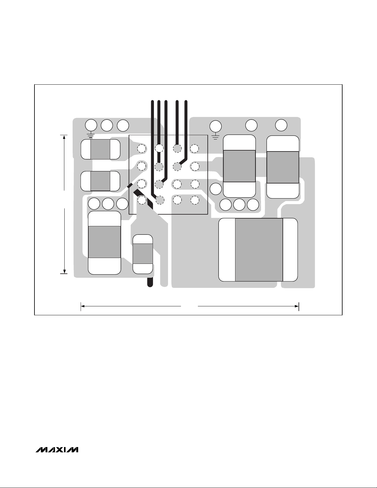
PCB Layout
High switching frequencies and relatively large peak
currents make the PCB layout a very important part of
design. Good design minimizes excessive EMI on the
feedback paths and voltage gradients in the ground
plane, resulting in a stable and well-regulated output.
Connect C
IN1
close to IN1A/IN1B and PGND. Connect
the inductor and output capacitor as close as possible
to the IC and keep their traces short, direct, and wide.
Keep noisy traces, such as the LX node, as short as
possible. Figure 3 illustrates an example PCB layout
and routing scheme.
Page 17
MAX8805Y/MAX8805Z
600mA PWM Step-Down Converters in
2mm x 2mm WLP for WCDMA PA Power
______________________________________________________________________________________ 17
Figure 3. Recommended PCB Layout
REFIN
PA_EN
EN1
HP
EN2
3.8mm
AGND
C
C
LDO2
BYP
PGND
C
IN1
C
IN2
VIN
C
LDO1
LDO1
LDO2
VPA
L
PA
C
PA
5.5mm
Page 18

MAX8805Y/MAX8805Z
600mA PWM Step-Down Converters in
2mm x 2mm WLP for WCDMA PA Power
18 ______________________________________________________________________________________
Figure 4. Typical Application Circuit Using LDOs for PA Enable/Bias
MAX8805Y/MAX8805Z
2MHz OR 4MHz
2.2μF
1μF
IN1A
IN1B
REFIN
PA_EN
HP
EN1
EN2
IN2
Li+ BATTERY
DAC
BASEBAND
PROCESSOR
GPIO
GPIO
GPIO
GPIO
BUCK
CONTROL
REF
LDO1
LX
PBA
PBB
PGND
REFBP
AGND
LDO1
1μH OR
2.2μH*
2.2μF
IN
PA1
EN/BIAS
0.22μF
0.1μF
LDO2
LDO2
*1μH FDK MIPS 2520D1R0
2.2μH FDK MIPF 2520D2R2
0.1μF
EN/BIAS
PA2
IN
Page 19

MAX8805Y/MAX8805Z
600mA PWM Step-Down Converters in
2mm x 2mm WLP for WCDMA PA Power
______________________________________________________________________________________ 19
Figure 5. Typical Application Circuit Using LDOs for RF Power
BASEBAND
PROCESSOR
Li+ BATTERY
DAC
GPIO
GPIO
GPIO
GPIO
2.2μF
2.2μF
IN1A
IN1B
REFIN
PA_EN
HP
EN1
EN2
IN2
MAX8805Y/MAX8805Z
2MHz OR 4MHz
BUCK
CONTROL
REF
LDO1
LX
PBA
PBB
PGND
REFBP
AGND
LDO1
1μH OR
2.2μH*
2.2μF
0.22μF
1μF
IN
IN
PA
RF RECEIVER
LDO2
*1μH FDK MIPS 2520D1R0
2.2μH FDK MIPF 2520D2R2
LDO2
1μF
IN
RF TRANSMITTER
Page 20
MAX8805Y/MAX8805Z
600mA PWM Step-Down Converters in
2mm x 2mm WLP for WCDMA PA Power
20 ______________________________________________________________________________________
Pin Configuration
Chip Information
PROCESS: BiCMOS
TOP VIEW
REFBP AGND
A1
LDO2
B1
IN2
C1
LDO1 PABEN1
D1
16-Bump, 2mm × 2mm WLP
A2 A3
PA_EN
B2
HP
C2
D2
(BUMP IN BOTTOM)
REFIN
EN2
B3
IN1B
C3
D3
PGND
A4
LX
B4
IN1A
C4
PAA
D4
Page 21
MAX8805Y/MAX8805Z
600mA PWM Step-Down Converters in
2mm x 2mm WLP for WCDMA PA Power
Maxim cannot assume responsibility for use of any circuitry other than circuitry entirely embodied in a Maxim product. No circuit patent licenses are
implied. Maxim reserves the right to change the circuitry and specifications without notice at any time.
Maxim Integrated Products, 120 San Gabriel Drive, Sunnyvale, CA 94086 408-737-7600 ____________________
21
© 2007 Maxim Integrated Products is a registered trademark of Maxim Integrated Products, Inc.
Package Information
(The package drawing(s) in this data sheet may not reflect the most current specifications. For the latest package outline information
go to www.maxim-ic.com/packages
.)
16L WLP.EPS
 Loading...