

Page 1

General Description
The MAX8775 is a dual, step-down, interleaved, fixedfrequency, switch-mode power-supply (SMPS) controller with synchronous rectification. It is intended for
GPU cores and I/O power generation in battery-powered systems. Flexible configuration allows the
MAX8775 to operate as two independent single-phase
regulators, or as one high-current two-phase regulator.
Configured in separate mode, the MAX8775 provides
power to two dynamic voltage rails, one for the GPU
core and the other for the I/O power rail. Configured in
combined mode, the MAX8775 functions as a twophase, high-current, single-output GPU core regulator,
powering the high-performance GPU engines used in
gaming machines and media center notebooks.
The REFIN voltage setting allows for multiple dynamic
output voltages required by the different GPU operating
and sleep states. Automatic fault blanking, forced-PWM
operation, and transition control are achieved by
detecting the voltage change at REFIN. Fixed-frequency operation with 180° out-of-phase interleaving minimizes input ripple current from the lowest input
voltages up to the 26V maximum input. Current-mode
control allows the use of low-ESR output capacitors.
Internal integrators maintain high output accuracy over
the full line-and-load range, in both forced-PWM mode
and pulse-skipping mode. True differential current
sensing provides accurate output current limit and current balance when operated in combined mode.
Independent on/off and skip control allows flexible
power sequencing and power management. Voltagecontrolled soft-start reduces inrush current. Soft-stop
gradually ramps the output voltage down, preventing
negative voltage dips.
Applications
2 to 4 Li+ Cells Battery-Powered Devices
Media Center and Gaming Notebooks
GPU and I/O Power Supplies
Tracking Output Power Supplies
Features
o Dual-Output, Fixed-Frequency, Current-Mode
Control
o Combinable Output for Higher Currents
o Dynamic Output Voltages with Automatic Fault
Blanking and Transition Control
o True Out-of-Phase Operation
o True Differential Current Sense for Accurate
Current Limit and Current Balance
o 4V to 26V Input Range
o 100kHz to 600kHz Switching Frequency
o 0.5V to 2.5V Adjustable Outputs
o Internal Integrator for High Output Accuracy
o Stable with Low-ESR Output Capacitors
o Independent Selectable PWM and Skip-Mode
Operation
o Independent Power-Good Outputs
o Soft-Start and Soft-Stop
o 2.5V Precision Reference
o < 1µA Typical Shutdown Current
MAX8775
Dual and Combinable Graphics Core
Controller for Notebook Computers
________________________________________________________________
Maxim Integrated Products
1
Pin Configuration
Ordering Information
19-0670; Rev 0; 11/06
For pricing, delivery, and ordering information, please contact Maxim/Dallas Direct! at
1-888-629-4642, or visit Maxim’s website at www.maxim-ic.com.
EVALUATION KIT
AVAILABLE
+
Denotes lead-free package.
PART TEMP RANGE
MAX8775ETJ+ -40°C to +85°C
PINPACKAGE
32 Thin QFN
5mm x 5mm
PKG
CODE
T3255-5
TOP VIEW
PGOOD1
DTRANS
SLEW1
DH1
ON1
CSL1
CSH1
SKIP1
BST1
2324 22 20 19 18
25
26
27
28
29
30
31
32
12
OVP1
DD
LX1
V
DL1
21
MAX8775
4567
3
CC
V
OSC
REFIN1
THIN QFN
5mm x 5mm
PGND
AGND
DL2
REF
LX2
17
REFIN2
8
BST2
OVP2
16
15
14
13
12
11
10
9
DH2
ON2
CSL2
CSH2
SKIP2
PGOOD2
CCI2
SLEW2
Page 2
MAX8775
Dual and Combinable Graphics Core
Controller for Notebook Computers
2 _______________________________________________________________________________________
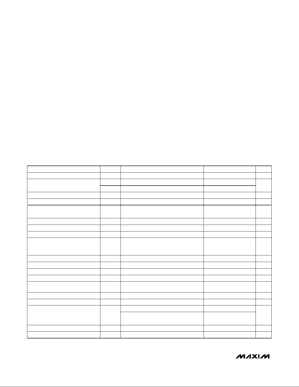
ABSOLUTE MAXIMUM RATINGS
ELECTRICAL CHARACTERISTICS
(Circuit of Figure 1, VIN= 12V, SKIP_ = PGND = AGND, ON_ = VCC= 5V, separate mode, TA= 0°C to +85°C, unless otherwise
noted. Typical values are at T
A
= +25°C.)
Stresses beyond those listed under “Absolute Maximum Ratings” may cause permanent damage to the device. These are stress ratings only, and functional
operation of the device at these or any other conditions beyond those indicated in the operational sections of the specifications is not implied. Exposure to
absolute maximum rating conditions for extended periods may affect device reliability.
V
DD,VCC
, CSH_, CSL_ to AGND............................-0.3V to +6V
ON_, SKIP_, PGOOD_ to AGND ..............................-0.3V to +6V
OVP_, REFIN_ to AGND ...........................................-0.3V to +6V
DTRANS to AGND ....................................................-0.3V to +6V
REF, OSC, SLEW_, CCI2 to AGND ...........-0.3V to (V
CC
+ 0.3V)
BST1, BST2 to AGND .............................................-0.3V to +36V
LX1 to BST1..............................................................-6V to +0.3V
LX2 to BST2..............................................................-6V to +0.3V
DH1 to LX1 ..............................................-0.3V to (V
BST
1
+ 0.3V)
DH2 to LX2 ..............................................-0.3V to (V
BST2
+ 0.3V)
DL1, DL2 to PGND .....................................-0.3V to (V
DD
+ 0.3V)
AGND to PGND .....................................................-0.3V to +0.3V
REF Short Circuit to AGND.........................................Continuous
REF Current ......................................................................+10mA
Continuous Power Dissipation (T
A
= +70°C)
32-Pin, 5mm x 5mm, Thin QFN
(derate 21.3mW/°C above +70°C).............................1702mW
Operating Temperature Range ...........................-40°C to +85°C
Junction Temperature......................................................+150°C
Storage Temperature Range .............................-65°C to +150°C
Lead Temperature (soldering, 10s) .................................+300°C
PARAMETER SYM B O L CONDITIONS MIN TYP MAX UNITS
INPUT SUPPLIES
Input Voltage Range
VCC Undervoltage Lockout Threshold V
Quiescent Supply Current (VCC)ICCCSL_ forced above their regulation points 1.5 2.5 mA
Quiescent Supply Current (VDD)I
Shutdown Supply Current (VCC)I
Shutdown Supply Current (VDD)I
SMPS CONTROLLERS
Output Voltage Accuracy
Output Voltage-Adjust Range V
RE FIN Op er ati ng V ol tag e- Ad j ust Rang eV
REFINOK Threshold Either SMPS 0.1 V
REFIN Transient Detection Threshold 5mV (typ) hysteresis ±25 mV
Combined-Mode Enabled Threshold V
DC Load Regulation Either SMPS, SKIP_ = VCC, zero to full load -0.1 %
Line Regulation Error Either SMPS, 4V < VIN < 26V 0.03 %/V
Switching-Frequency Accuracy
(Note 3)
Maximum Duty Factor D
Minimum On-Time t
V
IN
V
BIASVCC
UVLO
DD
C C (S H D N)
D D (S H D N)
V
REFIN_
V
CSL_
CSL_
REFIN_
REFIN2
f
OSC
MAX
ONMIN
, V
DD
Rising edge, 50mV typical hysteresis 4.1 4.25 4.5 V
CSL_ forced above their regulation points,
SKIP mode
ON1 = ON2 = GND < 1 5 µA
ON1 = ON2 = GND < 1 5 µA
With respect to REFIN_,
REFIN_ = 0.5V to 2.5V,
SKIP_ = V
Either SMPS (Note 2) 0.5 2.5 V
Either SMPS (Note 2) 0.5 2.5 V
R
= 143kΩ (f
OSC
R
= 71.5kΩ (f
OSC
432kΩ (f
(Note 4) 150 ns
OSC
426
4.5 5.5
< 1 5 µA
-5 0 +5 mV
or GND (Note 1)
CC
V
-1VCC -
CC
= 300kHz nominal) -10 +10
OSC
= 600kHz nominal) to
OSC
= 99kHz nominal)
3
-15 +15
91 93 %
0.4
V
V
%
Page 3

MAX8775
Dual and Combinable Graphics Core
Controller for Notebook Computers
_______________________________________________________________________________________ 3
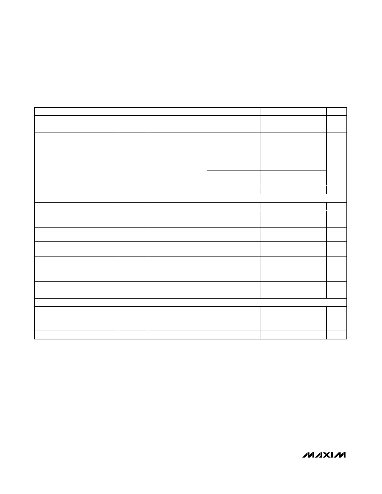
ELECTRICAL CHARACTERISTICS (continued)
(Circuit of Figure 1, VIN= 12V, SKIP_ = PGND = AGND, ON_ = VCC= 5V, separate mode, TA= 0°C to +85°C, unless otherwise
noted. Typical values are at T
A
= +25°C.)
Idle Mode is a trademark of Maxim Integrated Products, Inc.
SMPS1 to SMPS2 Phase Shift SMPS2 starts after SMPS1
Slew-Rate Current
CURRENT LIMIT
Current-Limit Threshold V
Current-Limit Threshold
(Negative)
Current-Limit Threshold
(Zero Crossing)
Idle Mode™ Threshold I
REFERENCE (REF)
Reference Voltage V
Refer ence S our ce Load Reg ul ati on ΔV
Reference Sink Load Regulation I
REF Lockout Voltage V
CURRENT BALANCE
Current-Balance Amplifier (GMI)
Offset
Current-Balance Amplifier (GMI)
Transconductance
FAULT DETECTION
OVP_ Adjust Range V
Outp ut Over vol tag e Tr i p Thr eshol d
Output Overvoltage Fault
Propagation Delay
Output Undervoltage Protection
Trip Threshold
Output Undevoltage Fault
Propagation Delay
Output Undervoltage Protection
Blanking Time
PGOOD_ Lower Trip Threshold
PGOOD_ Propagation Delay t
PARAMETER SYMBOL CONDITIONS MIN TYP MAX UNITS
50 %
180 Deg
I
SLEW_
I
SLEWSS_
LIMIT
V
NEG
V
MIN
REF
R E F ( U V L O)
OVP_
t
OVP
t
UVP
t
BLANK
PGOOD
During transition 4.0 4.75 5.5
Startup and shutdown 0.70 0.95 1.20
V
_ - V
CSH
V
_ - V
CSH
V
ZX
REFIREF
_ Falling edge, 50mV overdrive 10 µs
_ - V
CSH
V
_ - V
CSH
VCC = 4.5V to 5.5V,
= 0
I
REF
= 0µA to 250µA 0.25 1.5 mV
= -50µA 6 mV
REF
Rising edge, hysteresis = 100mV 2.3 V
[V(CSH1,CSL1) - V(CSH2,CSL2)] at I
/Δ[V(CSH1,CSL1) - V(CSH2,CSL2)],
ΔI
CCI
= V
V
CCI
V(CSH_,CSL_) = -60.0mV to +60.0mV
Rising edge measured at CSL_,
with respect to OVP_ set voltage
50mV overdrive 10 µs
Falling edge measured at CSL_,
with respect to error comparator threshold
50mV overdrive 10 µs
From rising edge of ON_ 6144 1/f
Falling edge measured at CSL_,
with respect to error comparator threshold,
hysteresis = 1%
_ 26 30 34 mV
CSL
_ , SKIP_ = V
CSL
_ , SKIP_ = GND 3 mV
CSL
_ , SKIP_ = GND 3.6 6 8.4 mV
CSL
= 0.5V to 2.5V, and
OUT
CC
TA = +25°C to +85°C 2.482 2.50 2.518
T
= 0°C to +85°C 2.475 2.50 2.525
A
= 0 -2 +2 mV
CCI
-43 -36 -29 mV
200 µS
0.5 2.5 V
180 200 220 mV
-325 300 -275 mV
-180 -150 -120 mV
µA
V
SW
Page 4
MAX8775
Dual and Combinable Graphics Core
Controller for Notebook Computers
4 _______________________________________________________________________________________
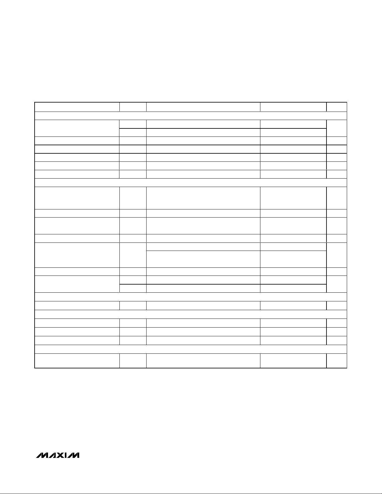
ELECTRICAL CHARACTERISTICS (continued)
(Circuit of Figure 1, VIN= 12V, SKIP_ = PGND = AGND, ON_ = VCC= 5V, separate mode, TA= 0°C to +85°C, unless otherwise
noted. Typical values are at T
A
= +25°C.)
(
)
)
PGOOD_ Output Low Voltage I
PGOOD_ Leakage Current I
PGOOD_ Transition Blanking
Time
Current-Balance Fault
Comparator Thresholds
Thermal-Shutdown Threshold T
GATE DRIVERS
DH_ Gate Driver On-Resistance R
DL_ Gate Driver On-Resistance
(Note 5)
DH_ Gate Driver Source/
Sink Current
DL_ Gate Driver Source Current
DL_ Gate Driver Sink Current I
Dead Time t
Internal Boost Diode Switch R
LX_, BST_ Leakage Current V
INPUTS AND OUTPUTS
Logic Input Current ON1, ON2, DTRANS, SKIP1, SKIP2 -1 +1 µA
Logic Input-High Threshold
Input Leakage Current CSH_, CSL_, 0V, or V
PARAMETER SYMBOL CONDITIONS MIN TYP MAX UNITS
ON
= 4mA 0.4 V
SINK
_ High state, PGOOD_ forced to 5.5V 1 µA
PGOOD
Measured from the time CSL_ reaches the
20 µs
SHDN
DH
R
DL
I
DH
I
DL
SOURCE
DL (SINK
DEAD
target voltage based on the slew rate set by
C
SLEW_
Lower threshold,
0.84V
V(CCI2, REF),
0.5V
≤ V
≤ 2.5V
FB
Hysteresis = 15°C +160 °C
BST_ - LX_ forced to 5V (Note 5) 1.5 5 Ω
DL_, high state 1.7 5
DL_, low state 0.6 3
DH_ forced to 2.5V, BST_ - LX_ forced to 5V 2 A
DL_ forced to 2.5V 1.7 A
DL_ forced to 2.5V 3.3 A
DL_ to DH_ 15 35
DH_ to DL_ 10 26
Measure with 10mA of current 6.5 9 Ω
_ = VLX_ = 28V < 2 20 µA
BST
ON1, ON2, DTRANS, SKIP1, SKIP2,
hysteresis = 225mV
DD
REF
Upper threshold,
1.2V
REF
2.0 2.2
2.9 3.0
1.2 1.7 2.2 V
-0.15 +0.15 µA
V
Ω
ns
Page 5
MAX8775
Dual and Combinable Graphics Core
Controller for Notebook Computers
_______________________________________________________________________________________ 5
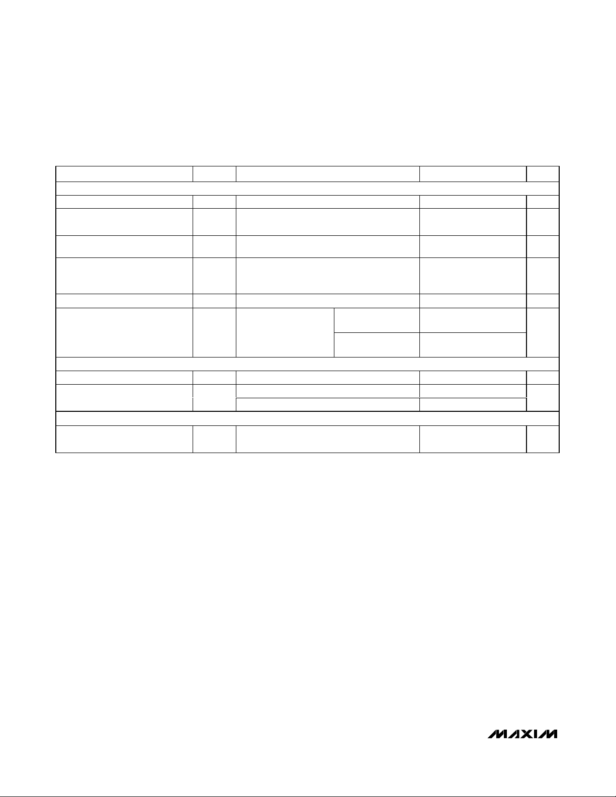
ELECTRICAL CHARACTERISTICS
(Circuit of Figure 1, VIN= 12V, SKIP_ = 0, ON_ = VCC= 5V, separate mode, TA= -40°C to +85°C, unless otherwise noted.) (Note 6)
INPUT SUPPLIES
Input Voltage Range
VCC Undervoltage Lockout
Quiescent Supply Current (VCC)ICCCSL_ forced above their regulation points 2.5 mA
Quiescent Supply Current (VDD)IDDCSL_ forced above their regulation points 5 µA
Shutdown Supply Current (VCC) ON1 = ON2 = GND 5 µA
Shutdown Supply Current (VDD) ON1 = ON2 = GND 5 µA
MAIN SMPS CONTROLLERS
PWM_ Output Voltage
Output Voltage Adjust Range V
REFIN Operating Voltage Adjust
Range
Combined Mode Enabled V
Switching Frequency Accuracy
(Note 2)
Maximum Duty Factor D
Slew-Rate Current
CURRENT LIMIT
Current-Limit Threshold V
REFERENCE (REF)
Reference Voltage V
Refer ence S our ce Load Reg ul ati on ΔV
Reference Sink Load Regulation I
CURRENT BALANCE
Current-Balance Amplifier (GMI)
Offset
PARAMETER SYMBOL CONDITIONS MIN TYP MAX UNITS
V
IN
V
BIASVCC
V
UVLO
V
-
REFIN_
V
CSL_
CSL_
V
REFIN_
REFIN2
f
OSC
MAX
I
SLEW_
I
SLEWSS_
LIMITVCSH
REF
REFIREF
, V
DD
Rising edge, 200mV typical hysteresis 4.1 4.5 V
With respect to REFIN_,
REFIN_ = 0.5V to 2.5V,
SKIP_ = V
Either SMPS (Note 2) 0.5 2.5 V
Either SMPS (Note 2) 0.5 2.5 V
R
OSC
R
OSC
432kΩ (f
During transition 3.75 5.50
Startup and shutdown 0.7 1.2
VCC = 4.5V to 5.5V, I
= 0µA to 250µA 2 mV
= -50µA 10 mV
REF
[V(CSH1,CSL1) - V(CSH2,CSL2)] at I
or GND (Note 1)
CC
= 143kΩ (f
= 71.5kΩ (f
= 99kHz nominal)
OSC
_ - V
CSL
= 300kHz nominal) -15 +15
OSC
= 600kHz nominal) to
OSC
_2535mV
= 0 2.462 2.538 V
REF
= 0 -3 +3 mV
CCI
426
4.5 5.5
-7.5 +7.5 mV
3V
-20 +20
90 %
%
µA
V
Page 6
MAX8775
Dual and Combinable Graphics Core
Controller for Notebook Computers
6 _______________________________________________________________________________________
Note 1: When the inductor is in continuous conduction, the output voltage has a DC regulation level lower than the error comparator
threshold by 50% of the ripple. In discontinuous conduction, the output voltage has a DC regulation level higher than the
error comparator threshold by 50% of the ripple.
Note 2: Operation below 0.5V but above the REFOK threshold is allowed, but the accuracy is not guaranteed.
Note 3: The MAX8775 cannot operate over all combinations of frequency, input voltage (V
IN
), and output voltage. For large input-tooutput differentials and high switching-frequency settings, the required on-time might be too short to maintain the regulation
specifications. Under these conditions, a lower operating frequency must be selected. The minimum on-time must be
greater than 150ns, regardless of the selected switching frequency. On-time and off-time specifications are measured from
the 50% point to the 50% point at the DH_ pin with LX_ = GND, VBST_ = 5V, and a 250pF capacitor connected from DH_ to
LX_. Actual in-circuit times may differ due to MOSFET switching speeds.
Note 4: Specifications are guaranteed by design, not production tested.
Note 5: Production testing limitations due to package handling require relaxed maximum on-resistance specifications for the
thin QFN package.
Note 6: Specifications to T
A
= -40°C to +85°C are guaranteed by design, not production tested.
ELECTRICAL CHARACTERISTICS (continued)
(Circuit of Figure 1, VIN= 12V, SKIP_ = 0, ON_ = VCC= 5V, separate mode, TA= -40°C to +85°C, unless otherwise noted.) (Note 6)
PARAMETER SYMBOL CONDITIONS MIN TYP MAX UNITS
FAULT DETECTION
OVP_ Adjust Range V
O utp ut O ver vol tag e Tr i p Thr eshol d
Output Undervoltage Protection
Trip Threshold
PGOOD_ Lower Trip Threshold
PGOOD_ Output Low Voltage I
Current-Balance Fault
Comparator Thresholds
GATE DRIVERS
DH_ Gate Driver On-Resistance R
DL_ Gate Driver On-Resistance
(Note 4)
INPUTS AND OUTPUTS
Logic Input-High Threshold
OVP_
DH
R
DL
Rising edge measured at CSL_,
with respect to OVP_ set voltage
Falling edge measured at CSL_,
with respect to error comparator threshold
Falling edge measured at CSL_
with respect to error comparator threshold,
hysteresis = 1%
= 4mA 0.4 V
SINK
Lower threshold,
0.84V
V(CCI2, REF),
0.5V ≤ V
BST_ - LX_ forced to 5V (Note 4) 5 Ω
DL_, high state 5
DL_, low state 3
ON1, ON2, DTRANS, SKIP1, SKIP2,
hysteresis = 225mV
≤ 2.5V
FB
REF
Upper threshold,
1.2V
REF
0.5 2.5 V
180 220 mV
275 325 mV
-180 -120 mV
2.0 2.2
2.9 3.1
1.2 2.2 V
mV
Ω
Page 7

MAX8775
Dual and Combinable Graphics Core
Controller for Notebook Computers
_______________________________________________________________________________________
7
Typical Operating Characteristics
(Circuit of Figure 1, V
IN =
12V, VDD= VCC= 5V, SKIP_ = GND, T
A =
+25°C, unless otherwise noted.)
1-PHASE EFFICIENCY
vs. LOAD CURRENT (V
100
90
80
70
EFFICIENCY (%)
60
50
40
0.1 100
LOAD CURRENT (A)
OUTPUT VOLTAGE vs. LOAD CURRENT
1.505
1.503
1.501
1.499
OUTPUT VOLTAGE (V)
1.497
1.495
030
LOAD CURRENT (A)
= 1.5V)
OUT
VIN = 7V, PWM
= 12V, PWM
V
IN
= 20V, PWM
V
IN
V
= 7V, SKIP
IN
= 12V, SKIP
V
IN
= 20V, SKIP
V
IN
101
VIN = 12V
= 1.5V
V
OUT
PWM MODE
SKIP MODE
20 2510 155
MAX8775 toc01
MAX8775 toc04
vs. LOAD CURRENT (V
100
90
80
70
EFFICIENCY (%)
60
50
40
0.1 100
vs. LOAD CURRENT (V
100
90
80
70
EFFICIENCY (%)
60
50
40
0.1 100
2-PHASE EFFICIENCY
LOAD CURRENT (A)
EFFICIENCY
LOAD CURRENT (A)
= 1.5V)
OUT
VIN = 7V, PWM
V
= 12V, PWM
IN
= 20V, PWM
V
IN
= 7V, SKIP
V
IN
= 12V, SKIP
V
IN
V
= 20V, SKIP
IN
101
= 1.2V)
OUT
= 12V
V
IN
= 1.2V
V
OUT
1-PHASE, PWM
2-PHASE, PWM
1-PHASE, SKIP
2-PHASE, SKIP
101
100
90
MAX8775 toc02
80
70
EFFICIENCY (%)
60
50
40
10
MAX8775 toc05
1
0.1
SUPPLY CURRENT (mA)
0.01
0.001
vs. LOAD CURRENT (V
EFFICIENCY
0.1 100
LOAD CURRENT (A)
NO-LOAD SUPPLY CURRENT
vs. INPUT VOLTAGE (SKIP MODE)
I
CC
I
DD
024
INPUT VOLTAGE (V)
OUT
= 12V
V
IN
= 1.5V
V
OUT
1-PHASE, PWM
2-PHASE, PWM
1-PHASE, SKIP
2-PHASE, SKIP
101
I
IN
16 208124
= 1.5V)
MAX8775 toc03
MAX8775 toc06
NO-LOAD SUPPLY CURRENT
vs. INPUT VOLTAGE (1-PHASE PWM MODE)
100
I
DD
10
SUPPLY CURRENT (mA)
I
1
024
CC
INPUT VOLTAGE (V)
I
IN
16 208124
100
MAX8775 toc07
SUPPLY CURRENT (mA)
NO-LOAD SUPPLY CURRENT
vs. INPUT VOLTAGE (2-PHASE PWM MODE)
I
DD
10
1
024
I
CC
INPUT VOLTAGE (V)
CURRENT-SENSE OFFSET
vs. LOAD CURRENT (2-PHASE PWM MODE)
1.0
MAX8775 toc08
I
IN
16 208124
0.5
0
-0.5
CURRENT BALANCE OFFSET (mV)
-1.0
030
LOAD CURRENT (A)
20 2510 155
MAX8775 toc09
Page 8
MAX8775
Dual and Combinable Graphics Core
Controller for Notebook Computers
8 _______________________________________________________________________________________
Typical Operating Characteristics (continued)
(Circuit of Figure 1, V
IN =
12V, VDD= VCC= 5V, SKIP_ = GND, T
A =
+25°C, unless otherwise noted.)
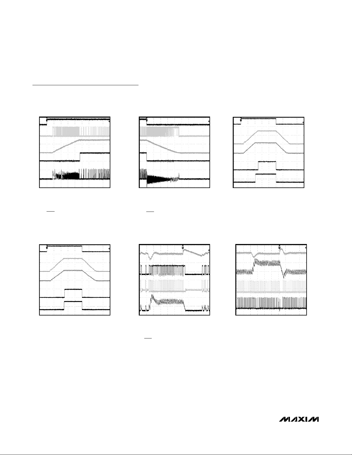
STARTUP WAVEFORMS
MAX8775 toc10
0
0
5A
200μs/div
0
0
A
B
D
C
E
0
D: PGOOD1, 5V/div
E: I
LX1
, 5A/div
A: ON1, 5V/div
B: DL1, 5V/div
C: V
OUT1
, 1V/div
SKIP1 = GND, R
LOAD1
= 1Ω, VIN = 12V
SHUTDOWN WAVEFORMS
MAX8775 toc11
0
1.5V
0
5A
0
0
A
B
D
C
E
0
D: PGOOD1, 5V/div
E: I
LX1
, 5A/div
A: ON1, 5V/div
B: DL1, 5V/div
C: V
OUT1
, 1V/div
SKIP1 = GND, R
LOAD1
= 1Ω, VIN = 12V
200μs/div
STARTUP/SHUTDOWN—
SAME SLEW RATE
0
0
5V
5V
0
0
A
B
D
C
E
0
D: PGOOD1, 5V/div
E: PGOOD2, 5V/div
A: ON1, ON2, 5V/div
B: V
OUT1
, 1V/div
C: V
OUT2
, 1V/div
C
SLEW1
= C
SLEW2
= 470pF
R
LOAD1
= R
LOAD2
= 1
Ω
400μs/div
MAX8775 toc12
STARTUP/SHUTDOWN—
SAME START TIME
MAX8775 toc13
0
0
5V
5V
0
400μs/div
0
A
B
D
C
E
0
D: PGOOD1, 5V/div
E: PGOOD2, 5V/div
A: ON1, ON2, 5V/div
B: V
OUT1
, 1V/div
C: V
OUT2
, 1V/div
C
SLEW1
= 470pF, C
SLEW2
= 600pF
R
LOAD1
= R
LOAD2
= 1
Ω
LOAD TRANSIENT (SEPARATE MODE)
MAX8775 toc14
0
10A
5V
0
20μs/div
1.2V
12V
A
B
D
C
0
C: LX1, 10V/div
D: I
LX1
, 10A/div
A: V
OUT1
, 100mV/div
B: DL1, 5V/div
V
IN
= 12V, V
OUT1
= 1.2V
SKIP1 = GND
I
OUT1
= 1A TO 11A TO 1A
LOAD TRANSIENT (COMBINED MODE)
MAX8775 toc15
0
10A
0
1.5V
12V
12V
A
B
D
C
0
C: LX1, 10V/div
D: LX2, 10V/div
A: V
OUT1
, 100mV/div
B: I
LX1
, 10A/div
VIN = 12V, V
OUT
= 1.5V
I
OUT1
= 5A TO 25A TO 5A
20μs/div
Page 9
MAX8775
Dual and Combinable Graphics Core
Controller for Notebook Computers
_______________________________________________________________________________________
9
Typical Operating Characteristics (continued)
(Circuit of Figure 1, V
IN =
12V, VDD= VCC= 5V, SKIP_ = GND, T
A =
+25°C, unless otherwise noted.)
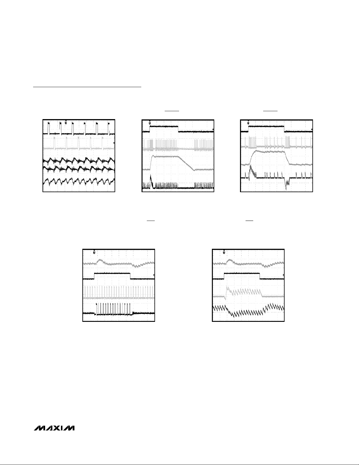
SWITCHING WAVEFORMS
MAX8775 toc16
12V
12V
1.5V
1.2V
12V
A
B
D
E
C
0
0
D: V
OUT2
, 50mV/div
E: V
IN
, 50mV/div
A: LX1, 10V/div
B: LX2, 10V/div
C: V
OUT1
, 50mV/div
VIN = 12V, V
OUT1
= 1.5V, V
OUT2
= 1.2V
I
OUT1
= 5A, I
OUT2
= 5A
2μs/div
REFIN TRANSITION WAVEFORMS
(DTRANS = V
CC
)
MAX8775 toc17
12V
1.5V
1.5V
1.2V
1.2V
10A
A
B
D
C
0
0
C: V
OUT1
, 200mV/div
D: I
LX1
, 10A/div
A: REFIN1, 500mV/div
B: LX1, 10A/div
V
IN
= 12V, V
REFIN1
= 1.2V TO 1.5V TO 1.2V
I
OUT1
= 1A
SKIP1 = GND
100μs/div
REFIN TRANSITION WAVEFORMS
(DTRANS = GND)
MAX8775 toc18
12V
1.5V
1.5V
1.2V
1.2V
A
B
D
C
0
0
C: V
OUT1
, 200mV/div
D: I
LX1
, 10A/div
A: REFIN1, 500mV/div
B: LX1, 10A/div
V
IN
= 12V, V
REFIN1
= 1.2V TO 1.5V TO 1.2V
I
OUT1
= 1A
SKIP1 = GND
40μs/div
COMBINED-MODE PHASE TRANSITION
MAX8775 toc19
12V
12V
1.2V
A
B
D
C
0
0
0
C: LX1, 10V/div
D: LX2, 10V/div
A: V
OUT
, 50mV/div
B: ON2, 5V/div
V
IN
= 12V, V
OUT
= 1.2V
I
OUT
= 10A
10μs/div
COMBINED-MODE PHASE TRANSITION
MAX8775 toc20
10A
10A
1.2V
A
B
D
C
0
0
0
C: I
LX2
, 10A/div
D: I
LX1
, 10A/div
A: V
OUT
, 50mV/div
B: ON2, 5V/div
V
IN
= 12V, V
OUT
= 1.2V
I
OUT
= 10A
10μs/div
Page 10

MAX8775
Dual and Combinable Graphics Core
Controller for Notebook Computers
10 ______________________________________________________________________________________
Pin Description
PIN NAME FUNCTION
SMPS1 Overvoltage Adjust Input. The overvoltage trip threshold for SMPS1 is 200mV above the voltage at OVP1.
1 OVP1
2 OSC
3 REFIN1
4V
5 AGND Analog Ground. Connect backside pad to AGND.
6 REF
7 REFIN2
8 OVP2
9 SLEW2
10 CCI2
11 PGOOD2
12 SKIP2
13 CSH2
14 CSL2
15 ON2
Connect OVP1 to V
OVP1 sets the overvoltage threshold for both phases in combined mode.
Oscillator Adjustment Input. Connect a resistor (R
(per phase):
A 71.5kΩ to 432kΩ corresponds to switching frequencies of 600kHz to 100kHz, respectively.
Ensure the minimum on-time requirement is met for the selected frequency.
SMPS1 External Reference Input. REFIN1 sets the output regulation voltage (V
REFIN1 sets the output regulation voltage in combined mode (V
Analog Supply Input. Connect to the system supply voltage (+4.5V to +5.5V) through a series 10Ω resistor.
CC
Bypass V
2.5V Reference Voltage Output. Bypass REF to AGND with a 0.1µF or greater ceramic capacitor. The maximum
value of this cap is 1µF. The reference can source up to 250µA. Loading REF degrades output-voltage accuracy
according to the REF load-regulation error (see Typical Operating Characteristics). The reference shuts down
when both ON1 and ON2 are low.
SMPS2 External Reference Input. REFIN2 sets the feedback regulation voltage (V
Connect REFIN2 to V
SMPS2 Overvoltage Adjust Input. The overvoltage trip threshold for SMPS2 is 200mV above the voltage at OVP2.
Connect OVP2 to V
Connect OVP2 to REF in combined mode when OVP is enabled.
Connect OVP2 to V
SMPS2 Slew-Rate Control. Connect a capacitor from SLEW2 to AGND to set the SMPS2 slew rate:
During startup and shutdown, SMPS2 ramps at 1/5 the programmed slew rate.
Connect SLEW2 to SLEW1 in combined mode.
Current-Balance Compensation for SMPS2. When combining SMPS1 and SMP2, connect a 47pF capacitor
between CCI2 and AGND.
Leave CCI2 open when operating SMPS1 and SMPS2 separately.
SMPS2 Open-Drain Power-Good Output. PGOOD2 is low when SMPS2 is more than 150mV below its regulation
threshold, when a 0V fault occurs, during soft-start, and in shutdown.
PGOOD2 is the current-balance fault indicator when operating in combined mode.
Low-Noise Mode Control for SMPS2. Connect SKIP2 to GND for normal Idle Mode (pulse-skipping) operation or
to V
CC
SKIP2 is ignored in combined mode.
Positive Current-Sense Input for SMPS2. Connect to the positive terminal of the current-sense element. Figure 10
describes two different current-sensing options.
Negative Current-Sense and Feedback Input for SMPS2. Connect to the negative terminal of the current-sense
element. CSL2 regulates to REFIN2. Figure 10 describes two different current-sensing options.
CSL2 regulates to REFIN1 in combined mode.
SMPS2 Enable Input. Drive ON2 high to enable SMPS2. Drive ON2 low to shut down SMPS2.
When both outputs are combined, ON1 is the master control input to enable/disable the combined output, while
ON2 enables/disables phase 2, allowing 1- or 2-phase operation.
to AGND with a 1µF or greater ceramic capacitor.
CC
for PWM mode (fixed frequency).
to disable OVP for SMPS1.
CC
) between OSC and AGND to set the switching frequency
OSC
= 300kHz x 143kΩ / R
f
OSC
to select combined mode. See OVP2 pin connection below.
CC
to disable OVP for SMPS2.
CC
in combined mode when OVP is disabled.
CC
Slew Rate (ΔV
OUT2
/ Δt) = I
CSL1
SLEW2
OSC
= V
/ C
CSL2
SLEW2
CSL1
= V
= V
REFIN1
CSL2
REFIN1
).
= V
).
REFIN2
).
Page 11

MAX8775
Dual and Combinable Graphics Core
Controller for Notebook Computers
______________________________________________________________________________________ 11
Pin Description (continued)
PIN NAME FUNCTION
16 DH2 High-Side Gate-Driver Output for SMPS2. DH2 swings from LX2 to BST2.
17 BST2
18 LX2
19 DL2 Low-Side Gate-Driver Output for SMPS2. DL2 swings from PGND to V
20 PGND Power Ground
21 V
22 DL1 Low-Side Gate-Driver Output for SMPS1. DL1 swings from PGND to VDD.
23 LX1
24 BST1
25 DH1 High-Side Gate-Driver Output for SMPS1. DH1 swings from LX1 to BST1.
26 ON1
27 CSL1
28 CSH1
29 SKIP1
30 P G OO D 1
31 DTRANS
32 SLEW1
— EP Exposed Backside Pad. Connect the exposed backside pad to AGND.
Boost Flying-Capacitor Connection for SMPS2. Connect to an external capacitor as shown in Figure 1. An optional
resistor in series with BST2 allows the DH2 turn-on current to be adjusted.
Inductor Connection for SMPS2. Connect LX2 to the switched side of the inductor. LX2 is the lower supply rail for
the DH2 high-side gate driver.
Supply Voltage Input for the DL_ Gate Drivers. Connect to a 5V supply. Bypass VDD to AGND with a 1µF or
DD
greater ceramic capacitor.
Inductor Connection for SMPS1. Connect LX1 to the switched side of the inductor. LX1 is the lower supply rail for
the DH1 high-side gate driver.
Boost Flying-Capacitor Connection for SMPS1. Connect to an external capacitor as shown in Figure 1. An optional
resistor in series with BST1 allows the DH1 turn-on current to be adjusted.
SMPS1 Enable Input. Drive ON1 high to enable SMPS1. Drive ON1 low to shut down SMPS1.
When both outputs are combined, ON1 is the master control signal to enable/disable the combined output, while
ON2 enables/disables phase 2, allowing 1- or 2-phase operation.
Negative Current-Sense and Feedback Input for SMPS1. Connect to the negative terminal of the current-sense
element. CSL1 regulates to REFIN1. Figure 10 describes two different current-sensing options.
Positive Current-Sense Input for SMPS1. Connect to the positive terminal of the current-sense element. Figure 10
describes two different current-sensing options.
Low-Noise Mode Control for SMPS1. Connect SKIP1 to GND for normal Idle Mode (pulse-skipping) operation or to
VCC for PWM mode (fixed frequency).
When both outputs are combined, SKIP2 is ignored and SKIP1 sets the skip function for both SMPS1 and SMPS2.
SMPS1 Open-Drain Power-Good Output. PGOOD1 is low when SMPS1 is more than 150mV below its regulation
threshold, when a 0V fault occurs, during soft-start, and in shutdown.
PGOOD1 is the voltage-regulation fault indicator when operating in combined mode.
Forced-Downward Transient Disable Input. Connect DTRANS to V
detection feature when operating in pulse-skipping mode, allowing the output to fall at a rate determined by the
load current and total output capacitance.
Connect DTRANS to AGND to enable the forced downward-transition detection feature.
SMPS1 Slew-Rate Control. Connect a capacitor from SLEW1 to AGND to set the SMPS1 slew rate:
Slew Rate (ΔV
During startup and shutdown, SMPS1 ramps at 1/5 the programmed slew rate.
In combined mode, the slew rate is set by both SLEW1 and SLEW2. Connect SLEW1 and SLEW2 together in
combined mode:
Combined Slew Rate (ΔV
OUT
/ Δt) = I
OUT1
/ Δt) = (I
SLEW1
to disable the forced-downward transition
CC
/ C
SLEW1
+ I
SLEW2
DD.
SLEW1
) / (C
SLEW1
+ C
SLEW2
)
Page 12

MAX8775
Detailed Description
The MAX8775 is a dual fixed-frequency step-down controller for low-voltage I/O and graphics core (GPU) supplies. It can be configured as two separate regulators
generating two independent outputs. Alternatively, the
MAX8775 can be configured in combined mode as a
two-phase, single-output, high-current regulator, powering the high-performance graphics cores used in
game machines and media center notebooks.
The standard applications circuit (Figure 1) generates
dynamically adjustable output voltages on both outputs. REFIN voltage setting allows for multiple dynamic
Dual and Combinable Graphics Core
Controller for Notebook Computers
12 ______________________________________________________________________________________
Figure 1. MAX8775 Separate Output Typical Operating Circuit
V
OUT1(L)
V
OUT1(H)
+5V
100kΩ
REF
C4
1μF
R8
R1
100kΩ
R3
249kΩ
150kΩ
C
REF
0.1μF
R
OSC
154kΩ
C
SLEW1
470pF
C
SLEW2
470pF
R9
100kΩ
R2
V
CC
REF
OSC
SLEW1
SLEW2
GND
DTRANS
PGOOD1
PGOOD2
OVP1
REFIN1
R7
10Ω
MAX8775
+5V
C3
V
DD
DH1
BST1
LX1
DL1
PGND
CSH1
CSL1
DH2
BST2
LX2
DL2
CSH2
CSL2
2.2μF
C
BST1
0.1μF
C1
2.2nF
C2
4.7nF
C
BST2
0.1μF
C5
2.2nF
C6
4.7nF
R10
150Ω
R12
150Ω
N
H1
N
D
L1
N
H2
N
D
L2
L1
L2
C
IN1
0.88μH
R11
10Ω
C
IN2
0.88μH
R13
10Ω
L1
L2
INPUT V
7V TO 20V
INPUT V
7V TO 20V
IN
R
1.5mΩ
IN
R
1.5mΩ
SENSE1
SENSE2
V
OUT1
1.5V/1.2V 15A
C
OUT1
(2) 330μF
V
OUT2
1.5V/1.2V 15A
C
OUT2
(2) 330μF
V
OUT2(L)
V
OUT2(H)
REF
R4
100kΩ
R6
249kΩ
150kΩ
CCI2
OVP2
REFIN2
R5
EP
ON1
ON2
SKIP1
SKIP2
NOT USED
ANALOG GROUND
POWER GROUND
SEE TABLE 1 FOR COMPONENT
SPECIFICATIONS.
Page 13

output voltages required by the different GPU operating
and sleep states. Automatic fault blanking, forced-PWM
operation, and transition control are achieved by
detecting the voltage change at REFIN.
The interleaved, fixed-frequency architecture provides
180° out-of-phase operation to reduce the input capacitance required to meet the RMS input-current ratings.
Each controller consists of a multi-input PWM comparator, high-side and low-side gate drivers, fault protection, power-good detection, soft-start, and shutdown
logic. Current-mode control allows the use of low-ESR
output capacitors.
In combined mode (Figure 2), phase 1 provides the
main voltage-control loop while phase 2 maintains the
MAX8775
Dual and Combinable Graphics Core
Controller for Notebook Computers
______________________________________________________________________________________ 13
Figure 2. MAX8775 Combined-Output Typical Operating Circuit
R7
10Ω
+5V
V
OUT(L)VOUT(H)
CONNECT REFIN2 TO VCC AND
OVP2 TO REF OR V
COMBINED-MODE OPERATION
100kΩ
REF
C4
1μF
R8
FOR
CC
R1
100kΩ
R3
249kΩ
REF
V
CC
C
0.1μF
R
154kΩ
C
SLEW
1000pF
R9
100kΩ
150kΩ
REF
OSC
R2
V
CC
REF
OSC
SLEW1
SLEW2
GND
DTRANS
MAX8775
PGOOD1
PGOOD2
OVP1
REFIN1
OVP2
REFIN2
EP
+5V
C3
V
DD
DH1
BST1
LX1
DL1
PGND
CSH1
CSL1
DH2
BST2
LX2
DL2
CSH2
CSL2
CCI2
ON1
ON2
SKIP1
SKIP2
2.2μF
C
BST1
0.1μF
C1
2.2nF
C2
4.7nF
C
BST2
0.1μF
C5
2.2nF
C6
4.7nF
R10
100Ω
R12
100Ω
C
CCI2
47pF
NOT USED
N
H1
N
N
N
D
L1
H2
D
L2
INPUT V
IN
7V TO 20V
C
IN1
L1
0.56μH
L1
R11
10Ω
C
IN2
L2
0.56μH
L2
R13
10Ω
SEE TABLE 1 FOR COMPONENT
SPECIFICATIONS.
INPUT V
IN
7V TO 20V
ANALOG GROUND
POWER GROUND
R
R
SENSE1
1.0mΩ
SENSE2
1.0mΩ
V
OUT
1.5V/1.2V 40A
C
OUT
(4) 330μF
Page 14

MAX8775
current balance. PGOOD1 indicates when the combined output is in regulation, while PGOOD2 indicates
the currents in both phases are balanced. Phase 2 can
be enabled or disabled based on the load current
required, maximizing efficiency over the full output current range.
Figure 3 is the MAX8775 functional block diagram.
Dual and Combinable Graphics Core
Controller for Notebook Computers
14 ______________________________________________________________________________________
Figure 3. MAX8775 Functional Block Diagram
V
REF
BST1
DH1
LX1
DL1
CSH1
CSL1
SKIP1
DTRANS
PGOOD1
REFIN1
SLEW1
ON1
OVP1
CC
2.5V REF
PWM
DRIVER
BLOCK
SLOPE COMP
POWER-
GOOD
REFIN
SOFT-START/
SOFT-STOP
OVP
Σ
4X
TRANS
REFIN
SLEW
MAX8775
V
IN
+5V BIAS
V
DD
OSC
BST2
DH2
LX2
DL2
CSH2
CSL2
SKIP2
CCI2
PGOOD 2
REFIN2
SLEW2
ON2
OVP2
SMPS 1
OSC
SMPS 2
AGND
PGND
Page 15

See Table 1 for component selections and Table 2 for
the component manufacturers.
SMPS 5V Bias Supply (VCCand VDD)
The MAX8775 SMPSs require a 5V bias supply in addition to the high-power input supply (battery or AC
adapter). VDDis the power rail for the MOSFET gate
drive, and VCCis the power rail for the IC. Connect the
external 4.5V to 5.5V supply directly to VDDand connect VDDto VCCthrough an RC filter, as shown in
Figure 1. The maximum supply current required is:
I
BIAS
= ICC+ fSW(Q
G(NL1)
+ Q
G1(NH1)+QG2(NL2)
+
Q
G2(NH2)
) = 1.8mA to 40mA
where ICCis 1.8mA, fSWis the switching frequency,
and QG_is the MOSFET data sheet’s total gate-charge
specification limits at VGS= 5V.
Reference (REF)
The 2.5V reference is accurate to ±1% over temperature and load, making REF useful as a precision system
reference. Bypass REF to GND with a 0.1µF or greater
ceramic capacitor. The reference sources up to 250µA
and sinks 50µA to support external loads.
MAX8775
Dual and Combinable Graphics Core
Controller for Notebook Computers
______________________________________________________________________________________ 15
Table 1. Component Selection for Standard Applications
Table 2. Component Suppliers
V
= 7V TO 24V
COMPONENT
MODE SEPARATE (FIGURE 1) SEPARATE COMBINED (FIGURE 2)
Switching Frequency 280kHz 280kHz 280kHz
C
, Input Capacitor
IN_
C
, Output
OUT_
Capacitor
NH_ High-Side
MOSFET
NL_ Low-Side MOSFET
DL_ Schottky Rectifier
L_ Inductor
Current-Sense R
SENSE
(2) 10µF, 25V
Taiyo Yuden TMK432BJ106KM
(2) 330µF, 6.3V, 7mΩ,
low-ESR capacitor
Panasonic EEFSD0D331XR
(1) Vishay/Siliconix
SI7634DP
(1) Vishay/Siliconix
SI7336ADP
3A, 40V Schottky diode
Central Semiconductor
CMSH3-40
0.88µH, 18A, 2.1mΩ
NEC/Tokin MPC1040LR88
1.5mΩ, 1W, 2512
_
Panasonic ERJM1WTJ1M5U
IN
= 1.0V - 1.5V / 15A
V
OUT1
V
= 7V TO 24V
IN
= 1.8V / 10A
V
OUT2
(1) 10µF, 25V
Taiyo Yuden TMK432BJ106KM
(1) 330µF, 6.3V, 7mΩ,
low-ESR capacitor
Panasonic EEFSD0D331XR
(1) International Rectifier
IRF7811W
(1) Vishay/Siliconix
SI7336ADP
3A, 40V Schottky diode
Central Semiconductor
CMSH3-40
1.8µH, 13.8A, 6.2mΩ
Sumida CDEP105(S)-1R8
2mΩ, 0.5W, 2010
Vishay WSL20102L000F
(4) 10µF, 25V
Taiyo Yuden TMK432BJ106KM
(4) 330µF, 6.3V, 7mΩ,
low-ESR capacitor
Panasonic EEFSD0D331XR
(1) Vishay/Siliconix
SI7634DP
(2) Vishay/Siliconix
SI7336ADP
3A, 40V Schottky diode
Central Semiconductor
CMSH3-40
0.56_H, 26A, 1.3mΩ
NEC/Tokin MPC1040LR56
Panasonic ETQP4LR56WFC
1.0mΩ, 1W, 2512
Panasonic ERJM1WTJ1M0U
V
= 7V TO 24V
IN
= 1.0V - 1.5V / 40A
V
OUT1
SUPPLIER WEBSITE SUPPLIER WEBSITE
AVX www.avx.com Panasonic www.panasonic.com/industrial
Central Semiconductor www.centralsemi.com Sanyo www.secc.co.jp
Coilcraft www.coilcraft.com Sumida www.sumida.com
Coiltronics www.coiltronics.com Taiyo Yuden www.t-yuden.com
Fairchild Semiconductor www.fairchildsemi.com TDK www.component.tdk.com
International Rectifier www.irf.com TOKO www.tokoam.com
Kemet www.kemet.com Vishay (Dale, Siliconix) www.vishay.com
Page 16

MAX8775
SMPS Detailed Description
SMPS Enable Controls (ON1, ON2)
ON1 and ON2 provide independent control of output
soft-start and soft-shutdown. This allows flexible control
of startup and shutdown sequencing. The outputs may
be started simultaneously, sequentially, or independently. To provide sequential startup, connect ON_ of one
regulator to PGOOD_ of the other. For example, with
ON1 connected to PGOOD2, OUT1 soft-starts after
OUT2 is in regulation. Additionally, tracking and ratiometric startup and shutdown can be achieved using the
SLEW_ capacitors. See the
Startup Sequencing
section.
When configured in combined mode (REFIN2 = V
CC
),
ON1 is the master control input that enables/disables
the combined output. ON2 enables/disables only the
2nd phase, allowing dynamic switching between onephase and two-phase operation.
Toggle ON_ low to clear the overvoltage, undervoltage,
and thermal-fault latches.
Soft-Start and Soft-Shutdown
Soft-start begins when ON_ is driven high and REF is in
regulation. During soft-start, the output is ramped up
from 0V to the final set voltage at 1/5 the slew rate programmed by the capacitor at the SLEW_ pin. This
reduces inrush current and provides a predictable
ramp-up time for power sequencing:
Soft-Start/Stop Slew Rate (ΔV
OUT_
/ Δt) =
I
SLEWSS_
/ C
SLEW_
where I
SLEWSS_
is 0.95µA (typ), and C
SLEW_
is the
capacitor across the SLEW_ pin and AGND. A 470pF
capacitor programs a slew rate of approximately
10mV/µs, and a soft-start, soft-shutdown slew rate of
approximately 2mV/µs.
Soft-shutdown begins after ON_ goes low, an output
undervoltage fault, or a thermal fault. During soft-shutdown, the output is ramped down to 0V at 1/5 the programmed slew rate, reducing negative inductor
currents that can cause negative voltages on the output. At the end of soft-shutdown, DL_ is driven high
until startup is again triggered by a rising edge of ON_.
The reference is turned off when both outputs have
been shut down.
When configured in separate mode, the two outputs are
independent. A fault at one output does not trigger
shutdown of the other.
Startup Sequencing
Individually programmable slew-rate control, on/off control, and power-good outputs allow flexible configuration
of the MAX8775 for different power-up sequencing. This
is useful in applications where one power rail needs to
come up after another, track another rail, or reach regulation at about the same time. Figures 4, 5, and 6 show
three configurations for startup sequencing.
Fixed-Frequency, Current-Mode PWM
Controller
The heart of each current-mode PWM controller is a
multi-input, open-loop comparator that sums three signals: the output voltage-error signal with respect to the
reference voltage, the current-sense signal, and the
slope compensation ramp (Figure 3). The MAX8775
uses a direct-summing configuration, approaching
ideal cycle-to-cycle control over the output voltage
Dual and Combinable Graphics Core
Controller for Notebook Computers
16 ______________________________________________________________________________________
Figure 4. MAX8775 Delayed Startup/Shutdown Timing
REF
C
= C
REF
SLEW2
REFIN1
MAX8775
REFIN2
AGND
SLEW1
SLEW2
ON1
1/5 PROGRAMMED
SLEW RATE
PGOOD1 = ON2
PGOOD2 20μs
DELAYED STARTUP/SHUTDOWN TIMING
REF
REFIN1
REFIN2
20μs
V
V
OUT1
OUT2
1/5 PROGRAMMED
SLEW RATE
C
SLEW1
Page 17

without a traditional error amplifier and the phase shift
associated with it.
The MAX8775 uses a relatively low loop gain, allowing
the use of lower cost output capacitors. The relative
gain of the voltage comparator to the current comparator is internally fixed at 4:1. The high current gain
results in stable operation even with low-output ESR
capacitors. An internal integrator corrects for any loadregulation error caused by the high current gain. The
low value of loop gain helps reduce output filter capacitor size and cost by shifting the unity-gain crossover
frequency to a lower level.
Frequency Selection (FSEL)
The OSC input programs the PWM mode switching frequency. Connect a resistor (R
OSC
) between OSC and
AGND to set the switching frequency (per phase):
fSW= 300kHz x 143kΩ / R
OSC
R
OSC
values between 71.5kΩ and 432kΩ correspond to
switching frequencies of 600kHz to 100kHz, respectively.
High-frequency (600kHz) operation optimizes the application for the smallest component size, trading off efficiency due to higher switching losses. This may be
acceptable in ultra-portable devices where the load
currents are lower. Low-frequency (100kHz) operation
offers the best overall efficiency at the expense of component size and board space.
MAX8775
Dual and Combinable Graphics Core
Controller for Notebook Computers
______________________________________________________________________________________ 17
Figure 5. MAX8775 Tracking Startup/Shutdown Timing
Figure 6. MAX8775 Ratiometric Startup/Shutdown Timing
ON1 = ON2
1/5 PROGRAMMED
SLEW RATE
PGOOD1
PGOOD2 20μs
TRACKING STARTUP/SHUTDOWN TIMING
REF
REFIN2
REFIN1
20μs
V
V
OUT2
OUT1
ON1 = ON2
1/5 PROGRAMMED
SLEW RATE
REF
REFIN2
REFIN1
V
OUT2
V
OUT1
1/5 PROGRAMMED
SLEW RATE
C
SLEW1
1/5 PROGRAMMED
SLEW RATE
= C
C
REF
SLEW2
C
REF
REF
REFIN2
MAX8775
REFIN1
AGND
SLEW1
SLEW2
REF
REFIN2
MAX8775
REFIN1
PGOOD1
PGOOD2 20μs
RATIOMETRIC STARTUP/SHUTDOWN TIMING
AGND
SLEW1
C
> C
SLEW1
SLEW2
SLEW2
Page 18

MAX8775
When selecting a switching frequency, the minimum ontime at the highest input voltage and lowest output voltage
must be greater than the 150ns (max) minimum on-time
specification in the
Electrical Characteristics
table:
V
OUT(MIN)
/ V
IN(MAX)
x TSW> t
ON(MIN)
A good rule is to choose a minimum on-time of at least
200ns.
When in pulse-skipping operation SKIP_ = GND, the
minimum on-time must take into consideration the time
needed for proper skip-mode operation. The on-time
for a skip pulse must be greater than the 150ns (max)
minimum on-time specification in the
Electrical
Characteristics
table:
Forced-PWM Mode
To maintain low-noise, fixed-frequency operation, drive
SKIP_ high to put the output into forced-PWM mode.
This disables the zero crossing comparator and allows
negative inductor current. During forced-PWM mode,
the switching frequency remains constant and the noload supply current is typically between 20mA and
40mA per phase, depending on external MOSFETs and
switching frequency.
Light-Load Operation Control (
SKIP_
)
The MAX8775 includes SKIP_ inputs, which enable the
corresponding outputs to operate in discontinuous
mode. Connect SKIP_ to GND to enable the zero-crossing comparators of either controller. When the zerocrossing comparator is enabled, the controller forces
DL_ low when the current-sense inputs detect zero
inductor current. This keeps the inductor from discharging the output capacitors and forces the controller to
skip pulses under light-load conditions to avoid overcharging the output. During skip mode, the VDDcurrent
consumption is reduced and efficiency is improved.
In combined mode, SKIP2 is unused, and SKIP1 sets the
operating mode for both phases. At very light loads, onephase and two-phase pulse-skipping operation have
about the same efficiency (see the Efficiency vs. Load
Current (V
OUT
=1.5V) graph in
Typical Operating
Characteristics
). Keeping the MAX8775 in two-phase skip
allows it to dynamically respond to a full-load transient
without requiring any system level-control signal to indicate the state of the GPU core.
Idle Mode Current-Sense Threshold
When pulse-skipping mode is enabled, the on-time of
the step-down controller terminates when the output
voltage exceeds the feedback threshold and when the
current-sense voltage exceeds the Idle Mode currentsense threshold. Under light-load conditions, the ontime duration depends solely on the Idle Mode
current-sense threshold, which is 20% (SKIP_ = GND)
of the full load current-limit threshold. This forces the
controller to source a minimum amount of power with
each cycle. To avoid overcharging the output, another
on-time cannot begin until the output voltage drops
below the feedback threshold. Since the zero-crossing
comparator prevents the switching regulator from sinking current, the controller must skip pulses. Therefore,
the controller regulates the valley of the output ripple
under light-load conditions.
Automatic Pulse-Skipping Crossover
In skip mode, an inherent automatic switchover to PFM
takes place at light loads (Figure 7). This switchover is
affected by a comparator that truncates the low-side
switch on-time at the inductor current’s zero crossing.
The zero-crossing comparator senses the inductor current across CSH_ and CSL_. Once V
CSH_
- V
CSL
_ drops
below the 3mV zero-crossing, current-sense threshold,
the comparator forces DL_ low. This mechanism causes
the threshold between pulse-skipping PFM and nonskipping PWM operation to coincide with the boundary
between continuous and discontinuous inductor-current
operation (also known as the “critical-conduction” point).
The load-current level at which PFM/PWM crossover
occurs, I
LOAD(SKIP)
, is determined by:
()
Dual and Combinable Graphics Core
Controller for Notebook Computers
18 ______________________________________________________________________________________
Figure 7. Pulse-Skipping/Discontinuous Crossover Point
RVV
LV
×
×−
SENSE I
()
N MAX
IMIN
OUT MIN
()
t
≥
ON MIN
()
INDUCTOR CURRENT
0
I
LOAD SKIP
()
t
ON(SKIP)
ON-TIME
()
−
VV V
IN OUT OUT
=
2
LV f
IN OSC
V
OUT
=
VINf
OSC
I
TIME
LOAD =
I
LOAD(SKIP)
I
LOAD(SKIP)
2
Page 19

In combined-mode operation, since the load is shared
between two phases, the load current at which
PFM/PWM crossover occurs is twice that of each
phase’s crossover current.
The switching waveforms may appear noisy and asynchronous when light loading causes pulse-skipping
operation, but this is a normal operating condition that
results in high light-load efficiency. Trade-offs in PFM
noise vs. light-load efficiency are made by varying the
inductance. Generally, low inductance produces a
broader efficiency vs. load curve, while higher values
result in higher full-load efficiency (assuming that the
coil resistance remains fixed) and less output voltage
ripple. Penalties for using higher inductor values
include larger physical size and degraded load-transient response (especially at low input-voltage levels).
Output Voltage
The MAX8775 regulates each output to the voltage set
at REFIN_ by sensing the CSL_ pin. Changing the voltage at REFIN_ allows the MAX8775 to be used in applications that require dynamic output voltage changes
between two or more set points. Figure 1 shows a
dynamically adjustable resistive voltage-divider network at REFIN_. Using system control signals to drive
the gate(s) of small-signal MOSFETs, resistors can be
switched in and out of the REFIN_ resistor-divider,
dynamically changing the voltage at REFIN_. The main
output voltage is determined by the following equation:
where R
EQ
is the equivalent resistance between
REFIN_ and ground, and R
TOP
is the resistance
between REFIN_ and REF (see Figures 1 and 2).
In combined mode (REFIN2 = VCC), REFIN1 sets the
voltage of the combined output.
Internal Integrator
The MAX8775 includes an internal transconductance
amplifier that integrates the feedback voltage and provides fine adjustment to the regulation voltage, allowing
accurate DC output-voltage regulation regardless of
the output ripple voltage. When the inductor conducts
continuously, the MAX8775 regulates the peak of the
output ripple. The internal integrator corrects for errors
due to ESR ripple voltage, slope compensation, and
current-sense load regulation, maintaining high DC
accuracy throughout the full load range, including lightload operation while in pulse-skipping mode.
Dynamic Output Voltages
The MAX8775 controller automatically detects upward
transitions of 25mV at REFIN_, enters forced-PWM
operation, and blanks the power-good thresholds until
20µs after the output reaches the new regulation target.
The MAX8775 slews the output up at a rate set by the
slew capacitor C
SLEW
_:
Slew Rate (ΔV
OUT_
/ Δt) = I
SLEW_
/ C
SLEW_
where I
SLEW_
is 4.75µA (typ), and C
SLEW_
is the
capacitor across the SLEW_ pin and AGND. A 470pF
capacitor programs a slew rate of approximately
10mV/µs.
Setting DTRANS low enables the automatic REFIN_
detection downward transitions (Figure 8). This feature
is especially useful as it allows the MAX8775 to be set
in the high-efficiency, pulse-skipping operation (SKIP_
= low), while voltage transitions are automatically taken
care of by the MAX8775. Forced downward transitions
return the energy from the output capacitors back to
the input reservoir.
MAX8775
Dual and Combinable Graphics Core
Controller for Notebook Computers
______________________________________________________________________________________ 19
Figure 8. REFIN Transition (Skip Mode, Downward Transition Enabled)
⎛
R
⎜
+
RR
⎝
EQ TOP
VV
OUT PWM REF
=
()
⎞
EQ
⎟
⎠
V
OUT(HIGH)
TRACKING OV 20μs
V
V
OUT(LOW)
REFIN(HIGH)
REFIN
MODE
DH
PGOOD
PULSE SKIP PULSE SKIP PULSE SKIP
REFIN(LOW)
FORCED-PWM FORCED-PWM
BLANK HIGH-Z BLANK HIGH-Z
OUT
20μs
OV THRESHOLD
PGOOD THRESHOLD
Page 20

MAX8775
Setting DTRANS high disables the forced downward
REFIN_ transition. This allows the output voltage to drift
down at a rate determined by the load current and the
total output capacitance (Figure 9). Downward transitions
in some systems are less critical from a timing standpoint
because the voltage is above the new lower target.
The power consumed in moving the output voltage to
the new lower level in a forced manner where the
energy is returned to the input with DTRANS low,
needs to be weighed against the higher leakage
power loss when the voltage drifts down with DTRANS
high. Since the efficiency calculations require complex workload duty factors to be taken into consideration, a simple setting of the DTRANS pin allows
testing and comparison in both modes to determine
which mode offers best efficiency. Table 3 is the
DTRANS operating modes truth table.
Combined-Mode Operation
Combined Mode (REFIN2 = VCC)
Combined-mode operation allows the MAX8775 to support even higher output currents by sharing the load
current between two phases, distributing the power
dissipation over several power components. The
MAX8775 is configured in combined mode by connecting
REFIN2 to V
CC
and OVP2 to REF or VCC. See Figure 2
for the combined-mode standard application schematic.
See the OVP2 connection requirements in the
Pin
Description
table.
Phase Transition (ON2)
While in combined mode, ON1 functions as the master
control signal that enables/disables the combined output. ON2 enables/disables only phase 2. This allows for
flexible power management where phase 2 can be disabled at lighter loads, operating at the most optimal
point of the efficiency curve. The MAX8775 does not
override the ON2 signal during startup and shutdown. If
ON2 is low during startup and shutdown, the MAX8775
operates only in one phase. Since the startup and shutdown slew rates are slow and the load currents are typically low, one-phase operation during startup and
shutdown might be possible. Actual system testing and
characterization of system load is required to guarantee
operation in this mode.
Dual and Combinable Graphics Core
Controller for Notebook Computers
20 ______________________________________________________________________________________
Figure 9. REFIN Transition (Skip Mode, Downward Transition Disabled)
Table 3. DTRANS Operating Modes Truth Table
V
OUT(HIGH)
V
OUT(LOW)
TARGET
FIXED OV THRESHOLD
OUTPUT DRAGGED
DOWN BY LOAD
20μs
PGOOD THRESHOLD
REFIN(HIGH)
REFIN
MODE
PGOOD
PULSE SKIP PULSE SKIP
DH
REFIN TRANSITION (SKIP MODE, DOWNWARD TRANSITION DISABLED)
REFIN(LOW)
BLANK HIGH-Z BLANK HIGH-Z
20μs
PWM MODE
DTRANS SKIP_ OPERATION DURING TRANSITION
SKIP_ sets the respective phase in forced-PWM mode.
XH
HL
LL
All positive and negative REFIN transitions are forced. PGOOD_ is blanked during the SLEW_ capacitor
transition + 20µs.
SKIP_ sets the respective phase in pulse-skipping mode.
Negative REFIN transitions are not forced, and the output voltage is discharged by the load.
SKIP_ sets the respective phase in pulse-skipping mode.
All positive and negative REFIN transitions are forced. PGOOD_ is blanked during the SLEW_ capacitor
transition + 20µs.
Page 21

While ON2 is low, PGOOD2 is blanked high impedance. When ON2 goes high again, the PGOOD2 current-balance comparator is reenabled.
Current Balance (CCI2)
CCI2 is the output of the current-balance transconductance amplifier. The voltage level on CCI2 allows fine
adjustment to the duty cycle of phase 2, keeping phase
2’s current in balance with phase 1. When V
CCI2
is 20%
above or below V
REF
, PGOOD2 goes low, indicating
the currents in the two phases are not balanced.
Place a 47pF capacitor from CCI2 to AGND to integrate
the current balance error. CCI2 is clamped to REF
when ON2 is low.
CCI2 is unused in separate mode, and can be left
unconnected.
Current-Limit Protection
The current-limit circuit uses differential current-sense
inputs (CSH_ and CSL_) to limit the peak inductor current. If the magnitude of the current-sense signal
exceeds the current-limit threshold, the PWM controller
turns off the high-side MOSFET (Figure 3). At the next
rising edge of the internal oscillator, the PWM controller
does not initiate a new cycle unless the current-sense
signal drops below the current-limit threshold. The
actual maximum load current is less than the peak current-limit threshold by an amount equal to half the
inductor ripple current. Therefore, the maximum load
capability is a function of the current-sense resistance,
inductor value, switching frequency, and duty cycle
(V
OUT/VIN
).
In forced-PWM mode, the MAX8775 also implements a
negative current limit to prevent excessive reverse
inductor currents when V
OUT
is sinking current. The
negative current-limit threshold is set to approximately
-120% of the positive current limit and tracks the positive current limit.
The current limit is fixed at 30mV (typ).
MOSFET Gate Drivers (DH_, DL_)
The DH_ and DL_ drivers are optimized for driving
moderate-sized high-side, and larger low-side power
MOSFETs. This is consistent with the low duty factor
seen in notebook applications, where a large VINV
OUT
differential exists. The high-side gate drivers
(DH_) source and sink 2A, and the low-side gate drivers (DL_) source 1.7A and sink 3.3A. This ensures
robust gate drive for high-current applications. The
DH_ floating high-side MOSFET drivers are powered by
charge pumps at BST_ while the DL_ synchronous-rectifier drivers are powered directly by the external 5V
supply (VDD).
Adaptive dead-time circuits monitor the DL_ and DH_
drivers and prevent either FET from turning on until the
other is fully off. The adaptive driver dead time allows
operation without shoot-through with a wide range of
MOSFETs, minimizing delays and maintaining efficiency. There must be a low-resistance, low-inductance
path from the DL_ and DH_ drivers to the MOSFET
gates for the adaptive dead-time circuits to work properly; otherwise, the sense circuitry in the MAX8775
interprets the MOSFET gates as “off” while charge
actually remains. Use very short, wide traces (50 mils to
100 mils wide if the MOSFET is 1in from the driver).
The internal pulldown transistor that drives DL_ low is
robust, with a 0.6Ω (typ) on-resistance. This helps prevent DL_ from being pulled up due to capacitive coupling from the drain to the gate of the low-side MOSFETs
when the inductor node (LX_) quickly switches from
ground to V
IN
. Applications with high input voltages and
long inductive driver traces may require additional gateto-source capacitance to ensure fast-rising LX_ edges,
do not pull up the low-side MOSFETs’ gate, causing
shoot-through currents. The capacitive coupling
between LX_ and DL_ created by the MOSFETs’ gate-todrain capacitance (C
RSS
), gate-to-source capacitance
(C
ISS
- C
RSS
), and additional board parasitics should not
exceed the following minimum threshold:
Lot-to-lot variation of the threshold voltage can cause
problems in marginal designs. Adding a resistor less
than 10Ω in series with BST_ might remedy the problem
by increasing the turn-on time of the high-side MOSFET
without degrading the turn-off time.
Power-Good Output (PGOOD_)
PGOOD_ is the open-drain output of a comparator that
continuously monitors each SMPS output voltage for
overvoltage and undervoltage conditions. PGOOD_ is
actively held low in shutdown (ON_ = GND), soft-start,
and soft-shutdown. Once the soft-start terminates,
PGOOD_ becomes high impedance as long as the output does not drop below 150mV from the nominal regulation voltage set by REFIN_. PGOOD_ goes low once
the output drops 150mV below its nominal regulation
point, an output overvoltage fault occurs, or ON_ is
pulled low. For a logic-level PGOOD_ output voltage,
connect an external pullup resistor between PGOOD_
and +5V or +3.3V. A 100kΩ pullup resistor works well in
most applications.
PGOOD_ is blanked high impedance during all transitions detected at REFIN_ until 20µs after the output
reaches the regulation voltage.
MAX8775
Dual and Combinable Graphics Core
Controller for Notebook Computers
______________________________________________________________________________________ 21
C
⎛
VV
>
GS TH IN
()
RSS
⎜
⎝
C
ISS
⎞
⎟
⎠
Page 22

MAX8775
In combined mode (REFIN2 = VCC), PGOOD1 indicates the output voltage is in regulation, while PGOOD2
indicates the currents between the two phases are in
balance. PGOOD2 is the output of a comparator that
monitors the voltage difference between CCI2 and REF.
Since CCI2 is the output of a transconductance amplifier, even small current imbalance over a long time causes CCI2 to go high or low, depending on the current
imbalance. Whenever CCI2 is 20% above or below REF
(CCI2 ≥ 3V or CCI2 ≤ 2V), PGOOD2 goes low, indicating the currents in the two phases are not balanced.
PGOOD2 is blanked high impedance during all transitions detected at REFIN_ until 20µs after the output
reaches the regulation voltage.
Fault Protection
Output Overvoltage Protection
The MAX8775 includes an OVP_ pin that allows flexible
setting of the overvoltage fault threshold. The overvoltage threshold is 200mV (typ) above the voltage at the
OVP_ pin. This simplifies the configuration, allowing the
OVP_ pin to be directly connected to REFIN_, eliminating
the need for extra resistors to set the overvoltage level.
If the output voltage of either SMPS rises 200mV above
its nominal regulation voltage, the corresponding controller sets its overvoltage fault latch, pulls PGOOD_
low, and forces DL_ high for the faulted side. The other
controller is not affected. If the condition that caused
the overvoltage persists (such as a shorted high-side
MOSFET), the battery fuse blows. Cycle V
CC
below 1V
or toggle both ON_ pins to clear the overvoltage fault
latch and restart the SMPS controller.
In combined mode (REFIN2 = VCC), OVP1 sets the
overvoltage fault threshold for the combined output,
while OVP2 is connected to REF when OVP is enabled,
and to V
CC
when OVP is disabled.
Output Undervoltage Protection
If the output voltage of either SMPS falls 300mV below
its regulation voltage, the corresponding controller sets
its undervoltage fault latch, pulls PGOOD_ low, and
begins soft-shutdown for the faulted side by pulsing
DL_. DH_ remains off during the soft-shutdown
sequence initiated by an undervoltage fault. The other
controller is not affected. After soft-shutdown has completed, the MAX8775 forces DL_ high and DH_ low.
Cycle V
CC
below 1V or toggle ON_ to clear the under-
voltage fault latch and restart the SMPS controller.
VCCPOR and UVLO
Power-on reset (POR) occurs when VCCrises above
approximately 2V, resetting the fault latch and preparing the PWM for operation. VCCundervoltage-lockout
(UVLO) circuitry inhibits switching, forces PGOOD_
low, and forces the DL_ gate drivers low.
If VCCdrops low enough to trip the UVLO comparator
while ON_ is high, the MAX8775 immediately forces
DH_ and DL_ low on both controllers. The output discharges to 0V at a rate dependent on the load and the
total output capacitance. This prevents negative output
voltages, eliminating the need for a Schottky diode to
GND at the output.
Dual and Combinable Graphics Core
Controller for Notebook Computers
22 ______________________________________________________________________________________
Table 4. Operating Modes Truth Table
MODE CONDITION DESCRIPTION
Power-Up VCC UVLO
Run ON1 or ON2 enabled Normal operation.
Output
Overvoltage
Protection (OVP)
Output
Undervoltage
Protection (UVP)
Shutdown
Thermal
Shutdown
Either output > 200mV
above nominal level
Either output < 300mV
below nominal level, UVP is
enabled 6144 clock cycles
(1/f
) after the output is
OSC
enabled (ON_ going high)
ON1 and ON2
are driven low
> +160°C
T
J
When ON_ is high, DL_ is forced low as V
UVLO threshold. DL_ is forced high when V
When the overvoltage comparator trips, the faulted side sets the OV latch, forcing
PGOOD_ low and DL_ high. An OV fault on one SMPS does not affect the
operation of the other SMPS.
The O V l atch i s cl ear ed b y cycl i ng V
When the undervoltage comparator trips, the faulted side sets the UV latch,
forcing PGOOD_ low and initiating the soft-shutdown sequence by pulsing only
DL_. DL_ goes low after soft-shutdown. A UV fault on one SMPS does not affect
the operation of the other SMPS.
The U V l atch i s cl ear ed b y cycl i ng V
DL_ stays low after soft-shutdown is completed.
All circuitry is shut down.
Exited by POR or cycling ON1 and ON2.
DL1 and DL2 remain low.
falls below the 3.95V (typ) falling
CC
falls below 1V (typ).
CC
b el ow 1V or cycl i ng b oth O N _ p i ns.
C C
b el ow 1V or cycl i ng the r esp ecti ve O N _ p i n.
C C
Page 23

Thermal-Fault Protection
The MAX8775 features a thermal-fault protection circuit.
When the junction temperature rises above +160°C, a
thermal sensor sets the fault latches, pulls PGOOD_
low, and shuts down both SMPS controllers using the
soft-shutdown sequence (see the
Soft-Start and Soft-
Shutdown
section). Cycle VCCbelow 1V or toggle ON1
and ON2 to clear the fault latches and restart the controllers after the junction temperature cools by 15°C.
Design Procedure
Firmly establish the input voltage range and maximum
load current before choosing a switching frequency
and inductor operating point (ripple-current ratio). The
primary design trade-off lies in choosing a good switching frequency and inductor operating point, and the following four factors dictate the rest of the design:
• Input Voltage Range. The maximum value
(V
IN(MAX)
) must accommodate the worst-case, high
AC-adapter voltage. The minimum value (V
IN(MIN)
)
must account for the lowest battery voltage after
drops due to connectors, fuses, and battery selector
switches. If there is a choice at all, lower input voltages result in better efficiency.
• Maximum Load Current. There are two values to
consider. The peak load current (I
LOAD(MAX)
)
determines the instantaneous component stresses
and filtering requirements and thus drives output
capacitor selection, inductor saturation rating, and
the design of the current-limit circuit. The continuous load current (I
LOAD
) determines the thermal
stresses and thus drives the selection of input
capacitors, MOSFETs, and other critical heat-contributing components.
• Switching Frequency. This choice determines the
basic trade-off between size and efficiency. The
optimal frequency is largely a function of maximum
input voltage, due to MOSFET switching losses that
are proportional to frequency and V
IN
2
. The optimum frequency is also a moving target, due to
rapid improvements in MOSFET technology that are
making higher frequencies more practical.
• Inductor Operating Point. This choice provides
trade-offs between size and efficiency and between
transient response and output ripple. Low inductor
values provide better transient response and smaller physical size, but also result in lower efficiency
and higher output ripple due to increased ripple
currents. The minimum practical inductor value is
one that causes the circuit to operate at the edge of
critical conduction (where the inductor current just
touches zero with every cycle at maximum load).
Inductor values lower than this grant no further sizereduction benefit. The optimum operating point is
usually found between 20% and 30% ripple current.
When pulse skipping (SKIP_ low and light loads),
the inductor value also determines the load-current
value at which PFM/PWM switchover occurs.
Inductor Selection
The per-phase switching frequency and inductor operating point determine the inductor value as follows:
For example: I
LOAD(MAX)
= 15A, VIN= 12V, V
OUT
=
1.5V, f
OSC
= 300kHz, 30% ripple current or LIR = 0.3:
Find a low-loss inductor having the lowest possible DC
resistance that fits in the allotted dimensions. For the
selected inductance value, the actual peak-to-peak
inductor ripple current (ΔI
INDUCTOR
) is defined by:
Ferrite cores are often the best choice, although powdered iron is inexpensive and can work well at 200kHz.
The core must be large enough not to saturate at the
peak inductor current (I
PEAK
):
Transient Response
The inductor ripple current also impacts transientresponse performance, especially at low VIN- V
OUT
differentials. Low inductor values allow the inductor
current to slew faster, replenishing charge removed
from the output filter capacitors by a sudden load step.
The total output voltage sag is the sum of the voltage
sag while the inductor is ramping up, and the voltage
sag before the next pulse can occur:
where D
MAX
is the maximum duty factor (see the
Electrical Characteristics
), T is the switching period (1 /
f
OSC
), and ΔT equals V
OUT
/ VINx T when in PWM
mode, or L x 0.2 x I
MAX
/ (VIN- V
OUT
) when in skip
V
LI
CVD V
ITT
C
SAG
LOAD MAX
OUT IN MAX OUT
LOAD MAX
OUT
=
()
×−
()
+
−
()
Δ
ΔΔ
()
()
2
2
MAX8775
Dual and Combinable Graphics Core
Controller for Notebook Computers
______________________________________________________________________________________ 23
L
12 300 15 0 3
ΔI
II
PEAK LOAD MAX
VVV
OUT IN OUT
L
=
V f I LIR
IN OSCLOAD MAX
VVV
18 12 18
×−
..
()
×××
V kHz A
INDUCTOR
=+
−
()
()
VVV
()
OUT IN OUT
=
Vf L
IN OSC
Δ
I
()
INDUCTOR
=
097
. μ
.
−
2
H=
Page 24

MAX8775
mode. The amount of overshoot during a full-load to noload transient due to stored inductor energy can be calculated as:
where N
PH
is 2 in combined mode when both phases
are active.
Setting the Current Limit
The minimum current-limit threshold must be great
enough to support the maximum load current when the
current limit is at the minimum tolerance value. The perphase peak inductor current occurs at I
LOAD(MAX)
plus
half the ripple current; therefore:
where N
PH
is 2 in combined mode, and I
LIMIT
equals the
minimum current-limit threshold voltage divided by the
current-sense resistance (R
SENSE_
). For the 30mV default
setting, the minimum current-limit threshold is 26mV.
The current-sense method (Figure 10) and magnitude
determine the achievable current-limit accuracy and
power loss. The sense resistor can be determined by:
R
SENSE_
= V
LIM_
/ I
LIMIT_
For the best current-sense accuracy and overcurrent
protection, use a 1% tolerance current-sense resistor
between the inductor and output as shown in Figure 10a.
This configuration constantly monitors the inductor current, allowing accurate current-limit protection. However,
the parasitic inductance of the current-sense resistor can
cause current-limit inaccuracies, especially when using
low-value inductors and current-sense resistors. This
parasitic inductance (L
ESL
) can be cancelled by adding
an RC circuit across the sense resistor with an equivalent
time constant:
Alternatively, low-cost applications that do not require
highly accurate current-limit protection may reduce the
overall power dissipation by connecting a series RC
circuit across the inductor (Figure 10b) with an equivalent time constant:
Dual and Combinable Graphics Core
Controller for Notebook Computers
24 ______________________________________________________________________________________
Figure 10. Current-Sense Configurations
IL
Δ
()
V
SOAR
LOAD MAX
≈
NC V
2
PH OUT OUT
2
()
I
LIMIT
I
()
LOAD MAX
>+
N
PH
⎛
⎜
⎝
I
Δ
INDUCTOR
2
⎞
⎟
⎠
N
H
N
L
MAX8775
DH_
LX_
DL_
PGND
INPUT (VIN)
C
IN
D
L
L
CR
EQ EQ
=
L
ESL
R
SENSE
SENSE RESISTOR
ESL
R
C
SENSE
EQ
C
OUT
CEQREQ =
R
L
ESL
SENSE
L
R
EQ
CSH_
CSL_
a) OUTPUT SERIES RESISTOR SENSING
INPUT (VIN)
C
DH_
LX_
MAX8775
b) LOSSLESS INDUCTOR SENSING
DL_
PGND
CSH_
CSL_
N
H
N
L
IN
D
L
R
1
INDUCTOR
L
R
DCR
R
2
C
EQ
C
OUT
RCS = R2 = R
R1 + R2
L
1 + 1
R
=
DCR
[
CEQ R1 R2
DCR
]
Page 25

and:
where RCSis the required current-sense resistance,
and R
DCR
is the inductor’s series DC resistance. Use
the worst-case inductance and R
DCR
values provided
by the inductor manufacturer, adding some margin for
the inductance drop over temperature and load.
Output Capacitor Selection
The output filter capacitor must have low enough equivalent series resistance (ESR) to meet output ripple and
load-transient requirements, yet have high enough ESR
to satisfy stability requirements. The output capacitance
must be high enough to absorb the inductor energy
while transitioning from full-load to no-load conditions
without tripping the overvoltage fault protection. When
using high-capacitance, low-ESR capacitors (see stability requirements), the filter capacitor’s ESR dominates the
output voltage ripple. Therefore, the output capacitor’s
size depends on the maximum ESR required to meet the
output voltage ripple (V
RIPPLE(P-P)
) specifications:
In Idle Mode, the inductor current becomes discontinuous,
with peak currents set by the Idle Mode current-sense
threshold (V
IDLE
= 0.2V
LIMIT
). In Idle Mode, the no-load
output ripple can be determined as follows:
The actual capacitance value required relates to the
physical size needed to achieve low ESR, as well as to
the chemistry of the capacitor technology. Thus, the
capacitor is usually selected by ESR and voltage rating
rather than by capacitance value (this is true of tantalums, OS-CONs, polymers, and other electrolytics).
When using low-capacity filter capacitors, such as
ceramic capacitors, size is usually determined by the
capacity needed to prevent V
SAG
and V
SOAR
from
causing problems during load transients. Generally,
once enough capacitance is added to meet the overshoot requirement, undershoot at the rising load edge
is no longer a problem (see the V
SAG
and V
SOAR
equa-
tions in the
Transient Response
section). However, lowcapacity filter capacitors typically have high ESR zeros
that may affect the overall stability (see the
Output
Capacitor Stability Considerations
section).
Output Capacitor Stability Considerations
Stability is determined by the value of the output zero
relative to the switching frequency. The boundary of
instability is given by the following equation:
where:
For a typical 300kHz application, the output zero frequency must be well below 95kHz, preferably below
50kHz. Tantalum and OS-CON capacitors in widespread use at the time of publication have typical ESR
zero frequencies of 25kHz. In the design example used
for inductor selection, the ESR needed to support
25mV
P-P
ripple is 25mV/1.5A = 16.7mΩ. One
330µF/2.5V Sanyo polymer (TPE) capacitor provides
7mΩ (max) ESR. Together with the 1.5mΩ currentsense resistors, the output zero is 25kHz, zero is
25kHz, well within the bounds of stability.
The MAX8775 is optimized for low-duty-cycle operations. Steady-state operation at 45% duty cycle or higher
is not recommended.
The easiest method for checking stability is to apply a
very fast zero-to-max load transient and carefully
observe the output voltage ripple envelope for overshoot and ringing. It can help to simultaneously monitor
the inductor current with an AC current probe. Do not
allow more than one cycle of ringing after the initial
step-response under/overshoot.
Input Capacitor Selection
The input capacitor must meet the RMS ripple current
requirement (I
RMS
) imposed by the switching currents.
For a single step-down converter, the RMS input ripple
current is defined by the output load current (I
OUT
),
input voltage, and output voltage, with the worst-case
condition occurring at VIN= 2V
OUT
:
For a dual +180° interleaved controller, the out-ofphase operation reduces the RMS input ripple current,
effectively lowering the input capacitance requirements. When both outputs operate with a duty cycle
less than 50% (VIN> 2V
OUT
), the RMS input ripple cur-
rent is defined by the following equation:
I
V
V
II I
V
V
II I
RMS
OUT
IN
OUT OUT IN
OUT
IN
OUT OUT IN
=
⎛
⎝
⎜
⎞
⎠
⎟
−
()
+
⎛
⎝
⎜
⎞
⎠
⎟
−
()
1
11
2
22
MAX8775
Dual and Combinable Graphics Core
Controller for Notebook Computers
______________________________________________________________________________________ 25
R
CS DCR
R
=
RR
+212
R
R
=×+
DCR
CRR
EQ
⎡
⎢
⎣
⎤
⎥
2
⎦
L
111
V R I LIR
RIPPLE P P ESR LOAD MAX() ( )−
=
V
RIPPLE P P
()−
VR
IDLE ESR
=
R
SENSE
R R and f
<≤2
ESR SENSE ESR
f
=
ESR
RRC
24()π
ESR SENSE OUT
1
+
f
SW
π
II
=
RMS OUT
VVV
OUT IN OUT
−
()
V
IN
Page 26

MAX8775
where IINis the average input current:
In combined mode (REFIN2 = VCC) with both phases
active, the input RMS current simplifies to:
For most applications, nontantalum chemistries (ceramic, aluminum, or OS-CON) are preferred due to their
resistance to power-up surge currents typical of systems with a mechanical switch or connector in series
with the input. Choose a capacitor that has less than
10°C temperature rise at the RMS input current for optimal reliability and lifetime.
Power-MOSFET Selection
Most of the following MOSFET guidelines focus on the
challenge of obtaining high load-current capability
when using high-voltage (> 20V) AC adapters. Lowcurrent applications usually require less attention.
The high-side MOSFET (NH) must be able to dissipate
the resistive losses plus the switching losses at both
V
IN(MIN)
and V
IN(MAX)
. Ideally, the losses at V
IN(MIN)
should be roughly equal to the losses at V
IN(MAX)
, with
lower losses in between. If the losses at V
IN(MIN)
are
significantly higher, consider increasing the size of NH.
Conversely, if the losses at V
IN(MAX)
are significantly
higher, consider reducing the size of NH. If VINdoes
not vary over a wide range, optimum efficiency is
achieved by selecting a high-side MOSFET (NH) that
has conduction losses equal to the switching losses.
Choose a low-side MOSFET (NL) that has the lowest
possible on-resistance (R
DS(ON)
), comes in a moderatesized package (i.e., 8-pin SO, DPAK, or D2PAK), and is
reasonably priced. Ensure that the MAX8775 DL_ gate
driver can supply sufficient current to support the gate
charge and the current injected into the parasitic drainto-gate capacitor caused by the high-side MOSFET
turning on; otherwise, cross-conduction problems can
occur. Switching losses are not an issue for the low-side
MOSFET since it is a zero-voltage switched device
when used in the step-down topology.
Power-MOSFET Dissipation
Worst-case conduction losses occur at the duty factor
extremes. For the high-side MOSFET (NH), the worstcase power dissipation due to resistance occurs at
minimum input voltage:
PD (NHResistive) =
Generally, use a small high-side MOSFET to reduce
switching losses at high input voltages. However, the
R
DS(ON)
required to stay within package power-dissipation limits often limits how small the MOSFET can be.
The optimum occurs when the switching losses equal
the conduction (R
DS(ON)
) losses. High-side switching
losses do not become an issue until the input is greater
than approximately 15V.
Calculating the power dissipation in high-side MOSFETs
(N
H
) due to switching losses is difficult, since it must
allow for difficult-to-quantify factors that influence the
turn-on and turn-off times. These factors include the
internal gate resistance, gate charge, threshold voltage,
source inductance, and PCB layout characteristics. The
following switching loss calculation provides only a very
rough estimate and is no substitute for breadboard
evaluation, preferably including verification using a thermocouple mounted on N
H
:
PD (N
H
Switching) =
where C
RSS
is the reverse transfer capacitance of NH,
and I
GATE
is the peak gate-drive source/sink current
(1A typ).
Switching losses in the high-side MOSFET can become
a heat problem when maximum AC adapter voltages
are applied, due to the squared term in the switchingloss equation (C x V
IN
2
x fSW). If the high-side MOSFET
chosen for adequate R
DS(ON)
at low battery voltages
becomes extraordinarily hot when subjected to
V
IN(MAX)
, consider choosing another MOSFET with
lower parasitic capacitance.
For the low-side MOSFET (NL), the worst-case power
dissipation always occurs at maximum battery voltage:
PD (NLResistive) =
The absolute worst case for MOSFET power dissipation
occurs under heavy overload conditions that are
greater than I
LOAD(MAX)
, but are not high enough to
exceed the current limit and cause the fault latch to trip.
To protect against this possibility, “overdesign” the circuit to tolerate:
⎣
⎦
Dual and Combinable Graphics Core
Controller for Notebook Computers
26 ______________________________________________________________________________________
V
⎛
I
=
IN
⎜
⎝
OUT
V
IN
⎞
1
I
OUT
⎟
⎠
⎛
+
1
⎜
⎝
V
OUT
⎞
2
I
OUT
2
⎟
⎠
V
IN
II
=
RMS OUT
V
⎛
OUT
⎜
⎝
V
IN
V
⎞
⎛
1
−
⎟
⎜
⎠
⎝
2
OUT
V
IN
⎞
⎟
⎠
V
⎛
⎜
⎝
⎞
OUT
IR
()
LOAD DS ON
⎟
⎠
V
IN
2
()
VIfIQ
⎛
() ()
IN MAX LOAD SW
⎜
⎝
CV f
+
GATE
()
OSS IN MAX SW
2
⎞
⎟
⎠
2
⎛
⎜
⎝
GSW
I
GATE
⎞
⎟
⎠
⎡
⎢
⎢
12−
⎛
⎜
V
⎝
IN MAX
V
OUT
()
⎤
⎞
IR
⎥
()
LOAD DS ON
⎟
⎠
⎥
()
Page 27

where I
LIMIT
is the peak current allowed by the currentlimit circuit, including threshold tolerance and senseresistance variation. The MOSFETs must have a
relatively large heatsink to handle the overload power
dissipation.
Choose a Schottky diode (D
L
) with a forward voltage
drop low enough to prevent the low-side MOSFET’s
body diode from turning on during the dead time.
Boost Capacitors
The boost capacitors (C
BST
) must be selected large
enough to handle the gate charging requirements of
the high-side MOSFETs. Typically, 0.1µF ceramic
capacitors work well for low-power applications driving
medium-sized MOSFETs. However, high-current applications driving large, high-side MOSFETs require boost
capacitors larger than 0.1µF. For these applications,
select the boost capacitors to avoid discharging the
capacitor more than 200mV while charging the highside MOSFETs’ gates:
where Q
GATE
is the total gate charge specified in the
high-side MOSFETs’ data sheet. For example, assume
the SI7634DP n-channel MOSFET is used on the high
side. According to the manufacturer’s data sheet, a single SI7634DP has a gate charge of 21nC (VGS= 5V).
Using the above equation, the required boost capacitance would be:
Selecting the closest standard value, this example
requires a 0.1µF ceramic capacitor.
Applications Information
Duty-Cycle Limits
Minimum Input Voltage
The minimum input operating voltage (dropout voltage)
is restricted by the maximum duty-cycle specification
(see the
Electrical Characteristics
table). However,
keep in mind that the transient performance gets worse
as the step-down regulators approach the dropout voltage, so bulk output capacitance must be added (see
the voltage sag and soar equations in the
Design
Procedure
section). The absolute point of dropout
occurs when the inductor current ramps down during
the off-time (ΔI
DOWN
) as much as it ramps up during
the on-time (ΔI
UP
). This results in a minimum operating
voltage defined by the following equation:
where V
CHG
and V
DIS
are the parasitic voltage drops in
the charge and discharge paths, respectively. A reasonable minimum value for h is 1.5, while the absolute
minimum input voltage is calculated with h = 1.
Maximum Input Voltage
The MAX8775 controller includes a minimum on-time
specification, which determines the maximum input
operating voltage that maintains the selected switching
frequency (see the
Electrical Characteristics
table).
Operation above this maximum input voltage results in
pulse-skipping operation, regardless of the operating
mode selected by SKIP_. At the beginning of each
cycle, if the output voltage is still above the feedback
threshold voltage, the controller does not trigger an ontime pulse, effectively skipping a cycle. This allows the
controller to maintain regulation above the maximum
input voltage, but forces the controller to effectively
operate with a lower switching frequency. This results
in an input threshold voltage at which the controller
begins to skip pulses (V
IN(SKIP)
):
where f
OSC
is the switching frequency selected by OSC.
PCB Layout Guidelines
Careful PCB layout is critical to achieving low switching
losses and clean, stable operation. The switching
power stage requires particular attention (Figure 11). If
possible, mount all the power components on the top
side of the board, with their ground terminals flush
against one another. Follow these guidelines for good
PCB layout:
• Keep the high-current paths short, especially at the
ground terminals. This practice is essential for stable, jitter-free operation.
• Keep the power traces and load connections short.
This practice is essential for high efficiency. Using
thick copper PCB (2oz vs. 1oz) can enhance fullload efficiency by 1% or more. Correctly routing
PCB traces is a difficult task that must be
approached in terms of fractions of centimeters,
MAX8775
Dual and Combinable Graphics Core
Controller for Notebook Computers
______________________________________________________________________________________ 27
I
Δ
⎛
II
=−
LOAD LIMIT
INDUCTOR
⎜
⎝
2
⎞
⎟
⎠
C
C
==
BST
Q
GATE
=
BST
200
mV
nC
13
200
mV
0 105. μ
F
VVVhDVV
IN MIN OUT CHG
1
=++ −
⎛
⎜
⎝
MAX
⎞
1
()
OUT DIS()
⎟
⎠
+
VV
IN SKIP OUT
⎛
⎜
⎝
1
ft
OSC ON MIN
=
()
⎞
⎟
⎠
()
Page 28

MAX8775
where a single mΩ of excess trace resistance causes a measurable efficiency penalty.
• Minimize current-sensing errors by connecting
CSH_ and CSL_ directly across the current-sense
resistor (R
SENSE_
).
• When trade-offs in trace lengths must be made, it is
preferable to allow the inductor charging path to be
made longer than the discharge path. For example,
it is better to allow some extra distance between the
input capacitors and the high-side MOSFET than to
allow distance between the inductor and the lowside MOSFET or between the inductor and the output filter capacitor.
• Route high-speed switching nodes (BST_, LX_, DH_,
and DL_) away from sensitive analog areas (REF,
REFIN_, CSH_, CSL_).
Layout Procedure
1) Place the power components first, with ground terminals adjacent (NL_ source, CIN, C
OUT
_, and DL_
anode). If possible, make all these connections on
the top layer with wide, copper-filled areas.
2) Mount the controller IC adjacent to the low-side
MOSFET, preferably on the back side opposite N
L_
and NH_to keep LX_, GND, DH_, and the DL_ gatedrive lines short and wide. The DL_ and DH_ gate
traces must be short and wide (50 mils to 100 mils
wide if the MOSFET is 1in from the controller IC) to
keep the driver impedance low and for proper
adaptive dead-time sensing.
3) Group the gate-drive components (BST_ capacitor,
VDDbypass capacitor) together near the controller IC.
4) Make the DC-DC controller ground connections as
shown in Figures 1, 2, and 11. This diagram can be
viewed as having two separate ground planes:
power ground, where all the high-power components go; and an analog ground plane for sensitive
analog components. The analog ground plane and
power ground plane must meet only at a single
point directly at the IC.
5) Connect the output power planes directly to the output filter capacitor positive and negative terminals
with multiple vias. Place the entire DC-DC converter
circuit as close to the load as is practical.
Dual and Combinable Graphics Core
Controller for Notebook Computers
28 ______________________________________________________________________________________
Page 29

MAX8775
Dual and Combinable Graphics Core
Controller for Notebook Computers
______________________________________________________________________________________ 29
Figure 11. PCB Layout
Chip Information
TRANSISTOR COUNT: 6372
PROCESS: BiCMOS
KELVIN SENSE VIAS
UNDER THE SENSE
RESISTOR
(SEE EVALUATION KIT)
R
INDUCTOR INDUCTOR
PHASE 1
OUTPUT 2
SENSE
C
OUT
C
IN
VIA TO POWER
GROUND
C
OUT
POWER GROUND
INPUT
OUTPUT 1
OUTCOUT
C
CONNECT GND AND PGND THE
CONTROLLER AT ONE POINT
ONLY AS SHOWN
(SEE EVALUATION KIT)
R
SENSE
IN
C
PHASE 2
KELVIN SENSE VIAS
UNDER THE SENSE
RESISTOR
CONNECT THE
EXPOSED PAD TO
ANALOG GND
REF BYPASS
CAPACITOR
VIA TO ANALOG
GROUND
BYPASS
V
CC
CAPACITOR
Page 30

MAX8775
Dual and Combinable Graphics Core
Controller for Notebook Computers
Maxim cannot assume responsibility for use of any circuitry other than circuitry entirely embodied in a Maxim product. No circuit patent licenses are
implied. Maxim reserves the right to change the circuitry and specifications without notice at any time.
30
____________________Maxim Integrated Products, 120 San Gabriel Drive, Sunnyvale, CA 94086 408-737-7600
© 2006 Maxim Integrated Products is a registered trademark of Maxim Integrated Products. Inc.
Package Information
(The package drawing(s) in this data sheet may not reflect the most current specifications. For the latest package outline information
go to www.maxim-ic.com/packages
.)
QFN THIN.EPS
 Loading...