

Page 1
General Description
The MAX8759 integrated cold-cathode fluorescent lamp
(CCFL) inverter controller is designed to drive CCFLs
using a full-bridge resonant inverter. The resonant operation ensures reliable striking and provides near-sinusoidal
waveforms over the entire input range. The controller
operates over a wide input-voltage range of 4.5V to 28V
with high power to light efficiency. The device also
includes safety features that effectively protect against
single-point fault conditions such as lamp-out, secondary
overvoltage, and secondary short-circuit faults.
The MAX8759 provides accurate lamp-current regulation (±2.5%) for superior CCFL inverter performance.
The lamp current is adjustable with an external resistor;
10:1 dimming range can be achieved by turning the
CCFL on and off using a digital pulse-width modulation
(DPWM) method, while maintaining the lamp-current
constant. The MAX8759 provides three mechanisms for
controlling brightness: 2-wire SMBus™-compatible
interface, external ambient-light sensor (ALS), or system PWM control. The MAX8759 supports Intel display
power-saving technology (DPST) to maximize battery
life. The device includes two lamp-current feedback
input pins that support dual-lamp applications with a
minimum number of external components.
The MAX8759 controls a full-bridge inverter for maximum efficiency and directly drives four external n-channel power MOSFETs. An internal 5.35V linear regulator
powers the MOSFET drivers and most of the internal
circuitry. The MAX8759 is available in a space-saving,
28-pin, thin QFN package and operates over a -40°C to
+85°C temperature range.
Applications
Notebooks
LCD Monitors
Automotive Infotainment
Features
♦ Accurate Dimming Control Using SMBus, PWM
Interface, or Ambient Light Sensor
♦ 10:1 Dimming Range with 256-Step Resolution
♦ Resonant-Mode Operation
Longer Lamp Life with Near Sinusoidal LampCurrent Waveform
Guaranteed Striking Capability
High-Power-to-Light Efficiency
♦ Wide Input-Voltage Range (4.5V to 28V)
♦ Input Feed-Forward for Excellent Line Rejection
♦ ±2.5% Lamp-Current Regulation
♦ Adjustable 1.5% Accurate DPWM Frequency
♦ Dual Lamp-Current Feedback Inputs
♦ Comprehensive Fault Protection
Secondary Voltage Limiting
Primary Current Limit with Lossless Sensing
Lamp-Out Protection with Adjustable Timeout
Secondary Short-Circuit Protection
♦ Small 28-Pin, 5mm x 5mm, Thin QFN Package
MAX8759
Low-Cost, SMBus, CCFL Backlight Controller
________________________________________________________________ Maxim Integrated Products 1
Ordering Information
MAX8759
Minimal Operating Circuit
19-3874; Rev 0; 10/05
For pricing, delivery, and ordering information, please contact Maxim/Dallas Direct! at
1-888-629-4642, or visit Maxim’s website at www.maxim-ic.com.
PART
TEMP RANGE
PINPACKAGE
PKG
CODE
MAX8759ETI+
5mm × 5mm
T2855-6
+ Denotes lead-free package.
*EP = Exposed pad.
Pin Configuration appears at end of data sheet.
SMBus is a trademark of Intel Corp.
-40°C to +85°C
28 Thin QFN-EP*
Page 2

MAX8759
Low-Cost, SMBus, CCFL Backlight Controller
2 _______________________________________________________________________________________
ABSOLUTE MAXIMUM RATINGS
ELECTRICAL CHARACTERISTICS
(Circuit of Figure 1, V
BATT
= 12V, VCC= V
DD,TA
= 0°C to +85°C. Typical values are at TA= +25°C, unless otherwise noted.)
Stresses beyond those listed under “Absolute Maximum Ratings” may cause permanent damage to the device. These are stress ratings only, and functional
operation of the device at these or any other conditions beyond those indicated in the operational sections of the specifications is not implied. Exposure to
absolute maximum rating conditions for extended periods may affect device reliability.
BATT to GND..........................................................-0.3V to +30V
BST1, BST2 to GND ...............................................-0.3V to +36V
BST1 to LX1, BST2 to LX2 ........................................-0.3V to +6V
FREQ, V
CC
, VDDto GND .........................................-0.3V to +6V
SDA, SCL to GND.....................................................-0.3V to +6V
ALS, COMP, PWMI, PWMO,
TFLT, DEL, VALS to GND.......................-0.3V to (V
CC
+ 0.3V)
GH1 to LX1 ..............................................-0.3V to (V
BST1
+ 0.3V)
GH2 to LX2 ..............................................-0.3V to (V
BST2
+ 0.3V)
GL1, GL2 to GND.......................................-0.3V to (V
DD
+ 0.3V)
IFB1, IFB2, ISEC, VFB to GND ....................................-3V to +6V
PGND1, PGND2 to GND .......................................-0.3V to +0.3V
Continuous Power Dissipation (TA= +70°C)
28-Pin Thin QFN 5mm x 5mm
(derate 21.3mW/°C above +70°C).............................1702mW
Operating Temperature Range ...........................-40°C to +85°C
Junction Temperature......................................................+150°C
Storage Temperature Range .............................-65°C to +150°C
Lead Temperature (soldering, 10s) .................................+300°C
PARAMETER CONDITIONS
MIN
TYP
MAX
UNITS
VCC = VDD = V
BATT
4.5 5.5
BATT Input Voltage Range
V
CC
= VDD = open 5.5
V
V
BATT
= 28V 2.5 5
BATT Quiescent Current
V
BATT
= VCC = 5V 5
mA
BATT Quiescent Current, Shutdown MAX8759 is disabled 0.1 2 µA
VCC Output Voltage, Normal Operation
MAX8759 is enabled, 6V < V
BATT
< 28V,
0 < I
LOAD
< 10mA
5.2
5.5 V
VCC Output Voltage, Shutdown MAX8759 is disabled, no load 3.5 4.3 5.5 V
VCC rising (leaving lockout) 4.3
VCC Undervoltage Lockout Threshold
V
CC
falling (entering lockout) 3.7
V
VCC Undervoltage Lockout Hysteresis 230 mV
VCC POR Threshold Rising edge
V
VCC POR Hysteresis 50 mV
GH1, GH2, GL1, GL2 On-Resistance,
Low State
I
TEST
= 100mA, VCC = VDD = 5V 3 6 Ω
GH1, GH2, GL1, GL2 On-Resistance,
High State
I
TEST
= 100mA, VCC = VDD = 5V 10 18 Ω
BST1, BST2 Leakage Current V
BST
_ = 12V, V
LX
_ = 7V 4 10 µA
Resonant Frequency Range Guaranteed by design 30 80 kHz
Minimum On-Time 350 500 700 ns
Maximum Off-Time 40 60 80 µs
Current-Limit Threshold LX1 - PGND1, LX2 - PGND2 415 430 445 mV
Zero-Current-Crossing Threshold LX1 - PGND1, LX2 - PGND2 3 8 13 mV
Current-Limit Leading-Edge Blanking 350 ns
IFB1, IFB2 Input-Voltage Range -3 +3 V
IFB1 Regulation Point 765 785 805 mV
IFB2 Regulation Point 780 800 820 mV
MAX8759 is enabled
28.0
5.35
1.75
Page 3
MAX8759
Low-Cost, SMBus, CCFL Backlight Controller
_______________________________________________________________________________________ 3
ELECTRICAL CHARACTERISTICS (continued)
(Circuit of Figure 1, V
BATT
= 12V, VCC= V
DD,TA
= 0°C to +85°C. Typical values are at TA= +25°C, unless otherwise noted.)
PARAMETER CONDITIONS
MIN
TYP
MAX
UNITS
0 < V
IFB1,2
< 3V -3 +3
IFB1, IFB2 Input Bias Current
-3V < V
IFB1,2
< 0
µA
IFB1, IFB2 Lamp-Out Threshold 575 600 625 mV
IFB1, IFB2 to COMP Transconductance 0.5V < V
COMP
< 4V 60 100 160 µS
COMP Output Impedance 61224MΩ
COMP Discharge Current During Overvoltage
or Overcurrent Fault
V
VFB
= 2.6V or V
ISEC
= 1.5V 500
µA
COMP Discharge Current During DPWM
Off-Time
V
COMP
= 1.5V 90 110 130 µA
DPWM Rising-to-Falling Ratio V
IFB1,2
= 0 2.5
ISEC Input Voltage Range -3 +3 V
ISEC Overcurrent Threshold
V
ISEC Input Bias Current V
ISEC
= 1.25V
µA
VFB Input Voltage Range -4 +4 V
VFB Input Impedance 150 300 450 MΩ
VFB Overvoltage Threshold 2.1 2.3 2.5 V
VFB Undervoltage Threshold 210 240 280 mV
VFB Undervoltage Delay R
FREQ
= 169kΩ 250 µs
R
FREQ
= 169kΩ, TA = +25°C to +85°C
213
R
FREQ
= 169kΩ
215
R
FREQ
= 340kΩ 106
DPWM Oscillator Frequency
R
FREQ
= 100kΩ 343
Hz
PWMO Output Impedance 20 40 60 kΩ
PWMI Input Low Voltage 0.7 V
PWMI Input High Voltage 2.1 V
PWMI Input Hysteresis 300 mV
PWMI Input Bias Current
µA
PWMI Input Frequency Range 5 50 kHz
PWMI Full-Range Accuracy 5 LSB
PWMI duty cycle = 100% 98 100
PWMI duty cycle = 50% 48 50 52PWMI Brightness Setting
PWMI duty cycle = 0% 9.7
%
ALS Full-Adjustment Range 0 1.8 V
ALS Full-Range Accuracy 5 LSB
ALS Input Bias Current
µA
VALS Output Voltage
MAX8759 is enabled, 6V < V
BATT
< 28V,
I
LOAD
= 1mA
V
VALS Leakage Current MAX8759 is disabled, VALS = GND -3 +3 µA
VALS On-Resistance MAX8759 is enabled 30 60 Ω
-230
1000 2000
1.18 1.21 1.26
-0.3 +0.3
207 210
205 210
-0.3 +0.3
-0.1 +0.1
5.10 5.30 5.50
10.0 10.3
Page 4
MAX8759
Low-Cost, SMBus, CCFL Backlight Controller
4 _______________________________________________________________________________________
ELECTRICAL CHARACTERISTICS (continued)
(Circuit of Figure 1, V
BATT
= 12V, VCC= V
DD,TA
= 0°C to +85°C. Typical values are at TA= +25°C, unless otherwise noted.)
PARAMETER CONDITIONS
UNITS
V
BATT
= 9V, R
THR
= 100kΩ 0
Zero-Crossing Delay
V
BATT
= 12V, R
THR
= 100kΩ
µs
Maximum Zero-Crossing Delay V
BATT
= 16V, R
THR
= 100kΩ 3.2 3.8 4.4 µs
DEL rising 4.5
DEL Disable Threshold
DEL falling 3.8
V
0.9 1.0 1.1
TFLT Charge Current
115 135 155
µA
TFLT Trip Threshold Rising edge 3.7 4 4.3 V
SDA, SCL, Input Low Voltage 0.7 V
SDA, SCL, Input High Voltage 2.1 V
SDA, SCL, Input Hysteresis 100 mV
SDA, SCL, Input Bias Current -1 +1 µA
SDA Output Low Sink Current V
SDA
= 0.4V 4 mA
SMBus Frequency 10 100 kHz
SMBus Free Time t
BUF
4.7 1 µs
SCL Serial Clock High Period t
HIGH
4µs
SCL Serial Clock Low Period t
LOW
4.7 µs
START Condition Setup Time t
SU:STA
4.7 µs
START Condition Hold Time t
HD:STA
4µs
STOP Condition Setup Time from SCL t
SU:STO
4µs
SDA Valid to SCL Rising-Edge Setup Time,
Slave Clocking in Data
t
SU:DAT
250 ns
SCL Falling Edge to SDA Transition t
HD:DAT
0ns
SCL Falling Edge to SDA Valid, Reading Out
Data
t
DV
200 ns
MIN TYP MAX
1.50 1.80 2.10
0.15 0.30
V
< 1.25V and V
ISEC
V
< 1.25V and V
ISEC
V
> 1.25V and V
ISEC
< 540mV; V
IFB
> 660mV; V
IFB
> 660mV; V
IFB
= 2V
FLT
= 2V -1.5 -1.2 -0.8
FLT
= 2V
FLT
Page 5
MAX8759
Low-Cost, SMBus, CCFL Backlight Controller
_______________________________________________________________________________________ 5
ELECTRICAL CHARACTERISTICS
(Circuit of Figure 1, V
BATT
= 12V, VCC= V
DD,TA
= -40°C to +85°C.) (Note 1)
PARAMETER CONDITIONS
MIN
TYP
MAX
UNITS
VCC = VDD = V
BATT
4.5 5.5
BATT Input Voltage Range
V
CC
= VDD = open 5.5
V
V
BATT
= 28V 5
BATT Quiescent Current
V
BATT
= VCC = 5V 5
mA
VCC Output Voltage, Normal Operation
MAX8759 is enabled, 6V < V
BATT
< 28V,
0 < I
LOAD
< 10mA
5.2 5.5 V
VCC Output Voltage, Shutdown MAX8759 is disabled, no load 3.5 5.5 V
VCC rising (leaving lockout) 4.3
VCC Undervoltage Lockout Threshold
V
CC
falling (entering lockout) 3.7
V
GH1, GH2, GL1, GL2 On-Resistance,
Low State
I
TEST
= 100mA, VCC = VDD = 5V 6 Ω
GH1, GH2, GL1, GL2 On-Resistance,
High State
I
TEST
= 100mA, VCC = VDD = 5V 18 Ω
Resonant Frequency Range Guaranteed by design 30 80 kHz
Minimum On-Time 350 700 ns
Maximum Off-Time 40 80 µs
Current-Limit Threshold LX1 - PGND1, LX2 - PGND2 410 450 mV
Zero-Current Crossing Threshold LX1 - PGND1, LX2 - PGND2 3 13 mV
IFB1, IFB2 Input Voltage Range -3 +3 V
IFB1 Regulation Point 760 810 mV
IFB2 Regulation Point 775 825 mV
IFB1, IFB2 Input Bias Current -3V < V
IFB1,2
< 0
µA
IFB1, IFB2 Lamp-Out Threshold 565 635 mV
IFB1, IFB2 to COMP Transconductance 0.5V < V
COMP
< 4V 60 160 µS
COMP Output Impedance 625MΩ
COMP Discharge Current During Overvoltage
or Overcurrent Fault
V
VFB
= 2.6V or V
ISEC
= 1.5V 500
µA
COMP Discharge Current During DPWM
Off-Time
V
COMP
= 1.5V 90 130 µA
ISEC Input Voltage Range -3 +3 V
ISEC Overcurrent Threshold
V
VFB Input Voltage Range -4 +4 V
VFB Input Impedance 150 450 MΩ
VFB Overvoltage Threshold 2.1 2.5 V
VFB Undervoltage Threshold 210 280 mV
DPWM Oscillator Frequency R
FREQ
= 169kΩ 203 217 Hz
PWMO Output Impedance 20 60 kΩ
MAX8759 is enabled
-230
1.18 1.26
28.0
2000
Page 6
MAX8759
Low-Cost, SMBus, CCFL Backlight Controller
6 _______________________________________________________________________________________
ELECTRICAL CHARACTERISTICS (continued)
(Circuit of Figure 1, V
BATT
= 12V, VCC= V
DD,TA
= -40°C to +85°C.) (Note 1)
PARAMETER CONDITIONS
UNITS
PWMI Input Low Voltage 0.7 V
PWMI Input High Voltage 2.1 V
PWMI Input Frequency Range 5 50 kHz
PWMI duty cycle = 100% 98
PWMI duty cycle = 50% 48 52PWMI Brightness Setting
PWMI duty cycle = 0% 9.7
%
ALS Full-Adjustment Range 0 1.8 V
VALS Output Voltage
MAX8759 is enabled, 6V < V
BATT
< 28V,
I
LOAD
= 1mA
V
VALS On-Resistance MAX8759 is enabled 60 Ω
V
BATT
= 9V, R
THR
= 100kΩ 0 0.3
Zero-Crossing Delay
V
BATT
= 12V, R
THR
= 100kΩ
µs
Maximum Zero-Crossing Delay V
BATT
= 16V, R
THR
= 100kΩ 3.2 4.4 µs
DEL rising 4.5
DEL Disable Threshold
DEL falling 3.9
V
0.8 1.2
TFLT Charge Current
115 155
µA
TFLT Trip Threshold Rising edge 3.7 4.3 V
SDA, SCL, Input Low Voltage 0.7 V
SDA, SCL, Input High Voltage 2.1 V
SDA Output Low-Sink Current V
SDA
= 0.4V 4 mA
SMBus Frequency 10 100 kHz
SMBus Free Time t
BUF
4.7 µs
SCL Serial Clock High Period t
HIGH
4µs
SCL Serial Clock Low Period t
LOW
4.7 µs
START Condition Setup Time t
SU:STA
4.7 µs
START Condition Hold Time t
HD:STA
4µs
STOP Condition Setup Time from SCL t
SU:STO
4µs
SDA Valid to SCL Rising-Edge Setup Time,
Slave Clocking in Data
t
SU:DAT
250 ns
SCL Falling Edge to SDA Transition t
HD:DAT
0ns
SCL Falling Edge to SDA Valid,
Reading Out Data
t
DV
200 ns
Note 1: Specifications to -40°C are guaranteed by design, not production tested.
MIN TYP MAX
5.10 5.50
V
< 1.25V and V
ISEC
V
< 1.25V and V
ISEC
V
> 1.25V and V
ISEC
< 540mV; V
IFB
> 660mV; V
IFB
> 660mV; V
IFB
= 2V
FLT
= 2V -1.5 -0.8
FLT
= 2V
FLT
1.50 2.10
10.3
Page 7

MAX8759
Low-Cost, SMBus, CCFL Backlight Controller
_______________________________________________________________________________________ 7
C
D
B
A
A: VFB, 2V/div
B: LX1, 10V/div
LOW-INPUT VOLTAGE OPERATION
(V
IN
= 8.0V)
MAX8759 toc01
10µs/div
C: LX2, 10V/div
D:IFB, 2V/div
C
D
B
A
A: VFB, 2V/div
B: LX1, 20V/div
HIGH-INPUT VOLTAGE OPERATION
(V
IN
= 20.0V)
MAX8759 toc02
10µs/div
C: LX2, 20V/div
D: IFB, 2V/div
C
D
B
A
A: V
IN
, 10V/div
B: COMP, 2V/div
LINE TRANSIENT RESPONSE
(8V TO 20V)
MAX8759 toc03
100µs/div
C: IFB, 2V/div
D: LX1, 20V/div
C
D
B
A
A: V
IN
, 10V/div
B: COMP, 2V/div
LINE TRANSIENT RESPONSE
(20V TO 8V)
MAX8759 toc04
100µs/div
C: IFB, 2V/div
D: LX1, 20V/div
C
B
A
A: VFB, 2V/div
B: COMP, 1V/div
MINIMUM BRIGHTNESS STARTUP WAVEFORM
(SMBus MODE, BRIGHTNESS REGISTER = 0x00)
MAX8759 toc05
2ms/div
C: IFB, 2V/div
C
B
A
A: VFB, 2V/div
B: COMP, 1V/div
MINIMUM BRIGHTNESS DPWM OPERATION
(SMBus MODE, BRIGHTNESS REGISTER = 0x00)
MAX8759 toc06
2ms/div
C: IFB, 2V/div
C
B
A
A: VFB, 2V/div
B: COMP, 1V/div
50% BRIGHTNESS DPWM OPERATION
(SMBus MODE, BRIGHTNESS REGISTER = 0x80)
MAX8759 toc07
2ms/div
C: IFB, 2V/div
C
B
A
A: VFB, 2V/div
B: COMP, 1V/div
DPWM SOFT-START
MAX8759 toc08
40µs/div
C: IFB, 2V/div
C
B
A
A: VFB, 2V/div
B: COMP, 1V/div
DPWM SOFT-STOP
MAX8759 toc09
40µs/div
C: IFB, 2V/div
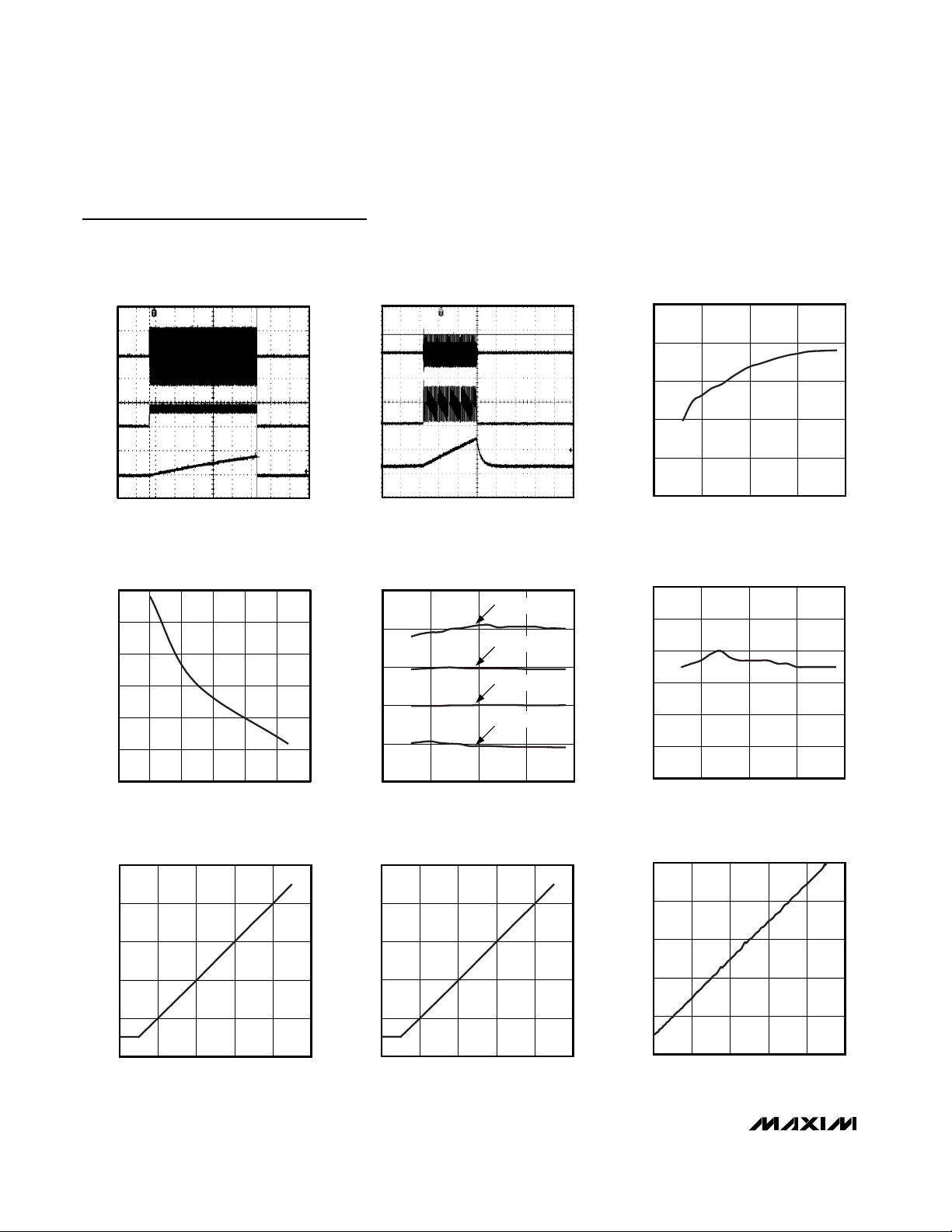
Typical Operating Characteristics
(Circuit of Figure 1, VIN= 12V, VCC= VDD, TA= +25°C, unless otherwise noted.)
Page 8
MAX8759
Low-Cost, SMBus, CCFL Backlight Controller
8 _______________________________________________________________________________________
Typical Operating Characteristics (continued)
(Circuit of Figure 1, VIN= 12V, VCC= VDD, TA= +25°C, unless otherwise noted.)
C
B
A
A: VFB, 2V/div
B: COMP, 500mV/div
OPEN-LAMP VOLTAGE
LIMITING AND TIMEOUT
MAX8759 toc010
200ms/div
C: TFLT, 5V/div
C
B
A
A: ISEC, 2V/div
B: COMP, 1V/div
SECONDARY SHORT-CIRCUIT PROTECTION
AND TIMEOUT
MAX8759 toc011
2ms/div
C: TFLT, 1V/div
30
40
60
50
70
80
SWITCHING FREQUENCY
vs. INPUT VOLTAGE
MAX8759 toc12
VIN (V)
SWITCHING FREQUENCY (kHz)
51510 20 25
50
150
100
250
200
300
350
DPWM FREQUENCY
vs. R
FREQ
MAX8759 toc13
R
FREQ
(kΩ)
DPWM FREQUENCY (Hz)
50 150 200100 250 300 350
3
4
6
5
7
8
RMS LAMP CURRENT
vs. INPUT VOLTAGE
MAX8759 toc14
INPUT VOLTAGE (V)
RMS LAMP CURRENT (mA)
51510 20 25
I
LAMP
= 7mA
I
LAMP
= 6mA
I
LAMP
= 5mA
I
LAMP
= 4mA
5.6
5.8
5.7
6.0
5.9
6.1
6.2
51510 20 25
RMS LAMP CURRENT (I
LAMP
= 6mA)
vs. INPUT VOLTAGE
MAX8759 toc15
INPUT VOLTAGE (V)
RMS LAMP CURRENT (mA)
0
20
60
40
80
100
00.40.2 0.6 0.8 1.0
NORMALIZED BRIGHTNESS
vs. PWMI DUTY CYCLE
MAX8759 toc17
PWMI DUTY RATIO
NORMALIZED BRIGHTNESS (%)
0
20
60
40
80
100
0 0.80.4 1.2 1.6 2.0
NORMALIZED BRIGHTNESS
vs. ALS VOLTAGE
MAX8759 toc18
V
ALS
(V)
NORMALIZED BRIGHTNESS (%)
0
20
60
40
80
100
04020 60 80 100
NORMALIZED BRIGHTNESS
vs. SMBus BRIGHTNESS SETTING
MAX8759 toc16
BRIGHTNESS SETTING (%)
NORMALIZED BRIGHTNESS (%)
Page 9

MAX8759
Low-Cost, SMBus, CCFL Backlight Controller
_______________________________________________________________________________________ 9
0
20
60
40
80
100
00.40.2 0.6 0.8 1.0
NORMALIZED BRIGHTNESS
vs. SMBus BRIGHTNESS AND PWMI DUTY CYCLE
MAX8759 toc19
PWMI DUTY RATIO
NORMALIZED BRIGHTNESS (%)
SMB = 0xFF
SMB = 0x80
0
0.2
0.6
0.4
0.8
1.0
00.40.2 0.6 0.8 1.0
NORMALIZED BRIGHTNESS
vs. ALS VOLTAGE AND PWMI DUTY CYCLE
MAX8759 toc20
PWMI DUTY RATIO
V
ALS
= 1.8V
V
ALS
= 1.8V
V
ALS
= 0.8V
B
A
ALS TRANSIENT RESPONSE
(ALSDEL1 = ALSDEL0 = 0)
MAX8759 toc21
A: ALS, 1V/div B: COMP, 1V/div
1s/div
5.30
5.31
5.33
5.32
5.34
5.35
VCC LINE REGULATION
MAX8759 toc22
INPUT VOLTAGE (V)
V
CC
VOLTAGE (V)
81612 20 24
5.30
5.31
5.33
5.32
5.34
5.35
042681012
VCC LOAD REGULATION
MAX8759 toc23
LOAD CURRENT (mA)
V
CC
VOLTAGE (V)
VIN = 24V
VIN = 12V
5.27
5.28
5.30
5.29
5.31
5.32
-40 0-20 20 406080
VCC VOLTAGE
vs. TEMPERATURE
MAX8759 toc24
TEMPERATURE (°C)
V
CC
VOLTAGE (V)
Typical Operating Characteristics (continued)
(Circuit of Figure 1, VIN= 12V, VCC= VDD, TA= +25°C, unless otherwise noted.)
Page 10
MAX8759
Low-Cost, SMBus, CCFL Backlight Controller
10 ______________________________________________________________________________________
Pin Description
PIN NAME FUNCTION
1 BATT
Supply Input. BATT is the input to the internal 5.35V linear regulator that powers the device. Bypass BATT
to GND with a 0.1µF ceramic capacitor.
2 SDA SMBus Serial Data Input
3 SCL SMBus Serial Clock Input
4 TFLT
Fault-Timer Adjustment Pin. Connect a capacitor from TFLT to GND to set the time-out periods for open-
lamp and secondary overcurrent faults.
5 VALS Ambient-Light-Sensor Supply Pin. Bypass VALS to GND with a 0.1µF capacitor.
6 ALS Ambient-Light-Sensor Input
7 PWMI DPST Control Input
8
DPST Buffer Output. Connect a capacitor between PWMO and GND. The capacitor forms a lowpass filter
with an internal 40kΩ (typ) resistor for filtering the DPST signal.
9 FREQ
Chopping-Frequency Adjustment Pin. Connect a resistor from FREQ to GND to set the DPWM frequency:
f
DPWM
= 210Hz × 169kΩ / R
FREQ
.
10 COMP
Transconductance Error Amplifier Output. A compensation capacitor connected between COMP and GND
sets the rise and fall time of the lamp-current envelope in DPWM operation.
11 DEL
Adaptive Zero-Crossing-Delay Adjustment Pin. Connect a resistor between DEL and GND to adjust the
range of the zero-crossing delay. Connecting DEL to V
CC
disables the zero-crossing delay function.
12 IFB1
Lamp-Current-Feedback Input. The IFB1 sense signal is internally full-wave rectified. IFB1 is compared
with IFB2 and the larger is used for lamp-current regulation. The average value of the rectified signal is
regulated to 785mV (typ) by controlling the on-time of high-side switch. An open-lamp fault is generated if
the peak voltage of IFB1 is below 600mV for a fault delay period set by TFLT.
13 IFB2
Lamp-Current-Feedback Input. The IFB2 sense signal is internally full-wave rectified. IFB1 is compared
with IFB2 and the larger is used for lamp-current regulation. The average value of the rectified signal is
regulated to 800mV (typ) by controlling the on-time of high-side switch. An open-lamp fault is generated if
the peak voltage of IFB2 is below 600mV for a fault-delay period set by TFLT. IFB2 input can be disabled
by connecting IFB2 to V
CC
.
14 VFB
Transformer Secondary Voltage-Feedback Input. A capacitive voltage-divider between the high-voltage
terminal of the CCFL tube and GND sets the maximum average lamp voltage during striking and lamp-out
fault. When the peak voltage on VFB exceeds the internal overvoltage threshold, the controller turns on an
internal current sink, discharging the COMP capacitor to limit the switch on-time. The VFB pin is also used
to detect a secondary undervoltage condition. If the peak voltage on VFB is below 230mV continuously for
250µs during the DPWM ON period, the MAX8759 shuts down.
15 ISEC
Transformer Secondary Current-Feedback Input. A current-sense resistor connected between the low-
voltage end of the transformer secondary and the ground sets the maximum secondary current during
short-circuit fault. When the peak voltage on ISEC exceeds the internal overcurrent threshold, the
controller turns on an internal current sink discharging the COMP capacitor.
16 LX1
GH1 Gate-Driver Return. LX1 is the input to the current-limit and zero-crossing comparators. The device
senses the voltage across the low-side MOSFET NL1 to detect primary current zero crossing and primary
overcurrent.
17 GH1 High-Side MOSFET NH1 Gate Driver Output
PWMO
Page 11

MAX8759
Low-Cost, SMBus, CCFL Backlight Controller
______________________________________________________________________________________ 11
PIN NAME FUNCTION
18 BST1 GH1 Gate-Driver Supply Input. Connect a 0.1µF capacitor from LX1 to BST1.
19
Power Ground. PGND1 is the return for the GL1 gate driver.
20 GL1 Low-Side MOSFET NL1 Gate Driver Output
21 V
DD
Low-Side Gate-Driver Supply Input. Connect V
DD
to the output of the internal linear regulator (VCC).
22 GL2 Low-Side MOSFET NL2 Gate-Driver Output
23
Power Ground. PGND2 is the return for the GL2 gate driver.
24 BST2 GH2 Gate-Driver Supply Input. Connect a 0.1µF capacitor from LX2 to BST2.
25 GH2 High-Side MOSFET NH2 Gate-Driver Output
26 LX2
GH2 Gate-Driver Return. LX2 is the input to the current-limit and zero-crossing comparators. The device
senses the voltage across the low-side MOSFET NL2 to detect primary current zero crossing and primary
overcurrent.
27 GND
Analog Ground. The ground return for V
CC
, REF, and other analog circuitry. Connect GND to PGND under
the IC at the IC’s backside exposed metal pad.
28 V
CC
5.35V/10mA Internal Linear-Regulator Output. VCC is the supply voltage for the device. Bypass VCC with a
0.47µF ceramic capacitor to GND.
—EPExposed Backside Pad. Connect PAD to GND.
Pin Description (continued)
PGND1
PGND2
Page 12

MAX8759
Low-Cost, SMBus, CCFL Backlight Controller
12 ______________________________________________________________________________________
N2A
19
24
21
21
C7
0.1µF
C8
0.47µF
C1
10µF
25V
C10
0.1µF
C11
0.1µF
C13
6.8nF
C6
68nF
C5
10nF
C4
10pF
3kV
C2
2.2µF
C3
2.2µF
T1
1:110
R1
150Ω
1%
CCFL
R2
3.9kΩ
C14
0.22µF
FDC6561AN
FDC6561AN
C9
0.47µF
C12
1µF
C15
0.1µF
R3
169kΩ
1%
V
CC
27
11
28
2
3
7
8
9
5
6
BATT
GND
DEL
V
CC
SDA
SCL
PWMI
PWMO
FREQ
VALS
ALS
18
17
16
26
20
23
22
25
12
13
V
CC
14
15
10
4
PGND1
BST2
V
DD
BST1
GH1
LX1
LX2
GL1
PGND2
GL2
GH2
IFB1
IFB2
VFB
ISEC
COMP
TFLT
N2B
N1A N1B
PWM INPUT
INPUT VOLTAGE
SMB_DATA
SMB_CLOCK
F1
2A
ALS SUPPLY
ALS OUTPUT
7.5V TO 24V
MAX8759
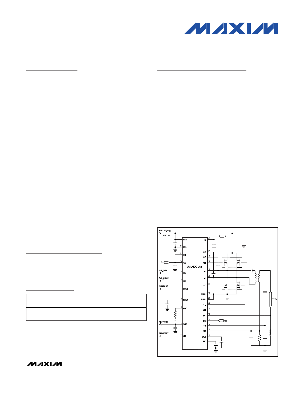
Figure 1. Typical MAX8759 Single-Lamp Operating Circuit
Page 13

MAX8759
Low-Cost, SMBus, CCFL Backlight Controller
______________________________________________________________________________________ 13
Typical Operating Circuit
The MAX8759 typical operating circuit (Figure 1) is a
single-lamp CCFL backlight inverter for notebook computer TFT LCD panels. The input voltage range of the
circuit is from 7.5V to 24V. The maximum RMS lamp
current is set to 6mA and the maximum RMS striking
voltage is set to 1800V. Table 1 lists some important
components and Table 2 lists the component suppliers’
contact information.
Detailed Description
The MAX8759 controls a full-bridge resonant inverter to
convert an unregulated DC input into a high-frequency
AC output for powering CCFLs. The resonant operation
maximizes striking capability and provides near-sinu-
soidal waveforms over the entire input range to improve
CCFL lifetime. The lamp brightness is adjusted by turning the lamp on and off with a DPWM signal. The
DPWM frequency can be accurately adjusted with a
resistor. The brightness of the lamp is proportional to
the duty cycle of the DPWM signal, which is controlled
either with a 2-wire SMBus-compatible interface, with
an external ALS, or with an external PWM signal. The
device also includes safety features that effectively protect against single-point fault conditions such as lampout and secondary short-circuit faults. An internal 5.35V
linear regulator powers the MOSFET drivers and most
of the internal circuitry. Figure 2 is the functional diagram of the MAX8759 and Figure 3 is the detailed diagram of the SMBus and ALS input block.
Resonant Operation
The MAX8759 drives four n-channel power MOSFETs
that make up the zero-voltage-switching (ZVS) fullbridge inverter as shown in Figure 4. Assume that NH1
and NL2 are on at the beginning of a switching cycle
as shown in Figure 4(a). The primary current flows
through MOSFET NH1, DC blocking capacitor C2, the
primary side of transformer T1, and MOSFET NL2.
During this interval, the primary current ramps up until
the controller turns off NH1. When NH1 is turned off, the
primary current forward biases the body diode of NL1,
which clamps the LX1 voltage just below ground as
shown in Figure 4(b). When the controller turns on NL1,
its drain-to-source voltage is near zero because its forward-biased body diode clamps the drain. Since NL2
is still on, the primary current flows through NL1, C2,
the primary side of T1, and NL2. Once the primary current drops to the minimum current threshold
(6mV/R
DS(ON)
), the controller turns off NL2. The
remaining energy in T1 charges up the LX2 node until
the body diode of NH2 is forward biased. When NH2
turns on, it does so with near-zero drain-to-source voltage. The primary current reverses polarity as shown in
Figure 4(c), beginning a new cycle with the current
flowing in the opposite direction, with NH2 and NL1 on.
The primary current ramps up until the controller turns
off NH2. When NH2 is turned off, the primary current
forward biases the body diode of NL2, which clamps
the LX2 voltage just below ground as shown in Figure
4(d). After the LX2 node goes low, the controller losslessly turns on NL2. Once the primary current drops to
the minimum current threshold, the controller turns off
NL1. The remaining energy charges up the LX1 node
until the body diode of NH1 is forward biased. Finally,
NH1 losslessly turns on, beginning a new cycle as
shown in Figure 4(a). Note that switching transitions on
all four power MOSFETs occur under ZVS conditions,
which reduces transient power losses and EMI.
DESIGNATION
DESCRIPTION
C1
10µF ±20%, 25V X5R ceramic capacitor
(1210)
Murata GRM32DR61E106M
TDK C3225X5R1E106M
C2, C3
2.2µF ±10%, 25V X5R ceramic capacitors
(0805)
Murata GRM21BR61E225K
TDK C2012X5R1E225K
C4
10pF ±10%, 3kV HV ceramic capacitor
(1808)
Kemet C1808C100KHGAC
TDK C4520C0G3F100F
NH1/2, NL1/2
Dual n-channel MOSFETs, 30V, 0.095Ω,
6-pin SOT23
Fairchild FDC6561AN
T1
CCFL transformer, 1:110 turns ratio
TMP UI9.8L type
Table 1. List of Important Components
SUPPLIER WEBSITE
Fairchild
Semiconductor
www.fairchildsemi.com
Kemet www.kemet.com
Murata www.murata.com
TDK www.components.tdk.com
TMP www.tmp.com
Table 2. Component Suppliers
Page 14

MAX8759
Low-Cost, SMBus, CCFL Backlight Controller
14 ______________________________________________________________________________________
Figure 2. MAX8759 Functional Diagram
BATT
GND
V
CC
VALS
ISEC
IFB1
IFB2
COMP
VFB
FREQ
SCL
SDA
ALS
PWMI
PWMO
2.3V
40kΩ
FW
FW
DWPM
OSC
SMBus
ALS
ADC
PWM
ADC
OV
COMP
LINEAR
REGULATOR
RDY
OC
COMP
1.21V
MAX
V
REF
OC
ERROR
AMP
1000µA 100µA
8-BIT
COUNTER
BRIGHTNESS
CONTROL
OC
BIAS
Z
X
600mV
DPWM
COMP
4.3V
MIN
EN
S
Q
R
OPEN-LAMP
DPWM
LATCH
S
Q
R
UVLO
COMPARATOR
COMP
RDY
BATT
MAX8759
V
CC
135µA
1µA
PWM
COMP
ILIM
COMP
230mV
VFB
FAULT
LATCH
S
Q
R
GATE-DRIVER
CONTROL
STATE
MACHINE
MUX
SHUTDOWN
DH
DH
DL
DL
4V
UV
COMP
MIN
TON
Q
R
TON FF
S
Q
400mV
ZERO-CROSS
ZX
DETECTIONS
DELAY BLOCK
AND
LX_
TFLT
BST1
GH1
LX1
BST2
GH2
LX2
VDD
GL1
PGND2
GL2
PGND1
DEL
Page 15

MAX8759
Low-Cost, SMBus, CCFL Backlight Controller
______________________________________________________________________________________ 15
Figure 3. MAX8759 SMBus and Ambient-Light-Sensor Input Block
ALS
STATUS
REGISTER
ALS
LOW-LIMIT
REGISTER
ALS
HIGH-LIMIT
REGISTER
ALS
CLAMP
BRIGHT
CONTROL
REGISTER
DEVICE
CONTROL
REGISTER
MUX
DIGITAL
MULTIPLIER
BUFFER
DIGITAL
POT
SMBus
INTERFACE
DPWM
SETTING
PWMI
SDA
SCL
0X04 0X00 0X010X060X05
MUX
"1"
PWMO
ALS
SMBus AND AMBIENT-LIGHT-SENSOR INPUT BLOCK
INVERTER
ON/OFF
MUX
PWM_SEL
ALS_CTL
PWM_MD
BUFFER
FAULT/
STATUS
REGISTER
0X02
OFFSET
A
D
A
D
A simplified CCFL inverter circuit is shown in Figure 5
(a). The full-bridge power stage is simplified and represented as a square-wave AC source. The resonant tank
circuit can be further simplified to Figure 5(b) by
removing the transformer. CSis the primary series
capacitor, CS’ is the series capacitance reflected to the
secondary, CPis the secondary parallel capacitor, N is
the transformer turns ratio, L is the transformer secondary leakage inductance, and RLis an idealized
resistance that models the CCFL in normal operation.
Figure 6 shows the frequency response of the resonant
tank’s voltage gain under different load conditions. The
primary series capacitor is 1µF, the secondary parallel
capacitor is 15pF, the transformer turns ratio is 1:93,
and the secondary leakage inductance is 260mH.
Notice that there are two peaks, fS,and fP, in the frequency response. The first peak fSis the series resonant peak determined by the secondary leakage
inductance (L) and the series capacitor reflected to the
secondary (C’S):
f
1
2LC
S
S
=
′
π
Page 16

MAX8759
The second peak fPis the parallel resonant peak determined by the secondary leakage inductance (L), the
parallel capacitor (CP), and the series capacitor reflected to the secondary (C’S):
The inverter is designed to operate between these two
resonant peaks. When the lamp is off, the operating
point of the resonant tank is close to the parallel resonant peak due to the lamp’s infinite impedance. The circuit displays the characteristics of a parallel-loaded
resonant converter. While in parallel-loaded resonant
operation, the inverter behaves like a voltage source to
generate the necessary striking voltage. Theoretically,
the output voltage of the resonant converter increases
until the lamp is ionized or until it reaches the IC’s secondary voltage limit. Once the lamp is ionized, the
equivalent load resistance decreases rapidly and the
operating point moves toward the series resonant peak.
While in series resonant operation, the inverter behaves
like a current source.
Lamp-Current Regulation
The MAX8759 uses a lamp-current control loop to regulate the current delivered to the CCFL. The heart of the
control loop is a transconductance error amplifier. The
f
L
CC
CC
P
SP
SP
=
′
′
+
1
2π
Low-Cost, SMBus, CCFL Backlight Controller
16 ______________________________________________________________________________________
T1
C2
V
BATT
(a)
NH1
ON
NL1
OFF
NH2
OFF
NL2
ON
LX2LX1
T1
C2
V
BATT
(b)
NH1
OFF
NL1
ON
NH2
OFF
NL2
ON
LX2LX1
T1
C2
V
BATT
(c)
NH1
OFF
NL1
ON
NH2
ON
NL2
OFF
LX2LX1
T1
C2
V
BATT
(d)
NH1
OFF
NL1
ON
NH2
OFF
NL2
ON
LX2LX1
(BODY DIODE TURNS ON FIRST) (BODY DIODE TURNS ON FIRST)
Figure 4. Resonant Operation
Page 17

AC lamp current is sensed with a resistor connected in
series with the low-voltage terminal of the lamp. The
MAX8759 has two lamp-current feedback inputs (IFB1
and IFB2) to support dual-lamp application. The voltages across the sense resistors are fed to the IFB1 and
IFB2 inputs and are internally full-wave rectified. The
transconductance error amplifier selects the higher one
of the two feedback signals and compares the rectified
voltage with an internal threshold to generate an error
current. The error current charges and discharges a
capacitor connected between COMP and ground to
create an error voltage (V
COMP
). V
COMP
is then compared with an internal ramp signal to set the high-side
MOSFET switch on-time (tON).
Feed-Forward Control
The MAX8759 is designed to maintain tight control of
the lamp current under all transient conditions. The
feed-forward control instantaneously adjusts the ontime for changes in input voltage (V
BATT
). This feature
provides immunity to input-voltage variations and simplifies loop compensation over wide input-voltage
ranges. The feed-forward control also improves the line
regulation for short DPWM on-times and makes startup
transients less dependent on the input voltage.
Feed-forward control is implemented by increasing the
internal voltage ramp rate for higher V
BATT
. This has
the effect of varying tONas a function of the input voltage while maintaining approximately the same signal
levels at V
COMP
. Since the required voltage change
across the compensation capacitor is minimal, the controller’s response to input voltage changes is essentially
instantaneous.
Lamp Startup
A CCFL is a gas-discharge lamp that is normally driven in
the avalanche mode. To start ionization in a nonionized
lamp, the applied voltage (striking voltage) must be
increased to the level required for the start of avalanche.
At low temperatures, the striking voltage can be several
times the typical operating voltage.
Because of the MAX8759’s resonant topology, the striking
voltage is guaranteed. Before the lamp is ionized, the
lamp impedance is infinite. The transformer secondary
leakage inductance and the high-voltage parallel capacitor determine the unloaded resonant frequency. Since the
unloaded resonant circuit has a high Q, it can generate
very high voltage across the lamp.
MAX8759
Low-Cost, SMBus, CCFL Backlight Controller
______________________________________________________________________________________ 17
AC
SOURCE
CCFL
C
P
L
C
S
1:N
(a)
AC
SOURCE
R
L
C
P
L
C'
S
=
(b)
C
S
N
2
Figure 5. Equivalent Resonant Tank Circuit
FREQUENCY (kHz)
VOLTAGE GAIN (V/V)
80604020
1
2
3
4
0
0 100
RL INCREASING
Figure 6. Frequency Response of the Resonant Tank
Page 18

MAX8759
Dimming Control
The MAX8759 controls the brightness of the CCFL by
“chopping” the lamp current on and off using a low-frequency (between 100Hz and 350Hz) DPWM signal.
The frequency of the internal DPWM oscillator is
adjustable through a resistor connected between the
FREQ pin and GND. The CCFL brightness is proportional to the DPWM duty cycle, which can be adjusted
from 10.15% to 100%.
In DPWM operation, the COMP voltage controls the
dynamics of the lamp-current envelope. At the beginning of the DPWM ON cycle, the average value of the
lamp-current feedback signal is below the regulation
point, so the transconductance error amplifier sources
current into the COMP capacitor. The switch on-time
(tON) gradually increases as V
COMP
rises, which provides soft-start. At the end of the DPWM ON cycle, the
MAX8759 turns on a 110µA internal current source. The
current source linearly discharges the COMP capacitor,
gradually decreasing tON, and providing soft-stop.
The DPWM frequency can be set with an external resistor. Connect a resistor between FREQ and GND. The
DPWM frequency is given by the following equation:
The adjustable range of the DPWM frequency is
between 100Hz and 350Hz (R
FREQ
is between 100kΩ
and 350kΩ).
The MAX8759 has three ways for brightness control.
The brightness can be controlled by a 2-wire serial
interface (SMBus), by an external PWM signal, or by an
external ambient-light sensor signal. There are five
operating modes, which can be selected by setting bits
1 to 3 in device control register 0x01 (see the SMBus
Register Definitions section for details).
ALS Mode
The MAX8759 can work with several types of ambientlight sensors. The ideal ambient-light sensors should
have a linear response to ambient light and should
have a spectral response equivalent to that of the
human eye. Ambient-light sensors must provide filtering
of low-frequency harmonics found in the electrical
spectrum of the many light sources. The ALS’s output
should be a DC analog voltage that is linearly proportional to the ambient luminance.
In ALS mode, the MAX8759 sets the brightness based
on the analog voltage on the ALS pin. The ALS pin is
connected to the output of an external ambient-light
sensor. The usable input-voltage range of the ALS pin
is 0 to 1.8V. The MAX8759 compares the ALS input
voltage against user-programmable low and high limits.
When the ALS input voltage is below the low limit, the
brightness is clamped to the ALS low limit. When the
ALS input voltage is above the high limit, the brightness is
clamped to the ALS high limit. If the minimum ALS setting
is below 10%, the brightness is clamped to 10%. Figure 7
shows the brightness change as a function of the ALS
voltage.
The ALS input voltage is sampled every DPWM period
and is loaded in ALS status register 0x04. The analog
voltage on the ALS pin is converted into an 8-bit digital
code. The total number of brightness levels is 256. One
step change results in a 0.391% change in the DPWM
duty cycle.
PWM Mode
In PWM mode, the MAX8759 sets the brightness based
on the duty cycle of the PWMI signal. The absolute minimum brightness is 10%. If the PWMI duty cycle is less
than 10%, the brightness stays at 10%. The frequency
range of the PWMI signal is between 5kHz and 50kHz
when the PWMO capacitor is 1µF.
SMBus Mode
In SMBus mode, the MAX8759 sets the brightness
based on the brightness control register (0x00). The
brightness control register contains 8 bits and supports
256 brightness levels. A setting of 0xFF for register
0x00 sets the inverter to the maximum brightness. A
setting of 0x00 for register 0x00 sets the inverter to the
minimum brightness (10%).
ALS with DPST Mode
In ALS with DPST mode, the MAX8759 sets the brightness based on the analog voltage on the ALS pin and
duty cycle at the PWMI pin. The MAX8759 lowers the
ALS brightness setting by an additional amount that is
proportional to the duty cycle of the PWMI signal. For
example, if the ALS brightness setting is 80% and the
duty cycle of PWMI signal is 60%, the resulting brightness setting is 80% x 60% = 48%.
SMBus with DPST Mode
In SMBus with DPST mode, the MAX8759 sets the
brightness based on the brightness control register
(0x00). The MAX8759 lowers the SMBus brightness setting by an additional amount that is proportional to the
duty cycle of the PWMI signal. For example, if the
brightness control register is set to 0x80 (corresponding to 50% brightness setting) and the duty cycle of the
PWMI signal is 60%, the resulting brightness setting is
50% x 60% = 30%.
fHzkR
DPWM FREQ
=×210 169 Ω/
Low-Cost, SMBus, CCFL Backlight Controller
18 ______________________________________________________________________________________
Page 19

Fault Protections
Lamp-Out Protection
For safety, the MAX8759 monitors the lamp-current
feedback inputs (IFB1 and IFB2) to detect faulty or
open CCFL tubes. As described in the Lamp-Current
Regulation section, the voltage on IFB1 and IFB2 is
internally full-wave rectified. If the rectified IFB1 or IFB2
voltage is below 600mV, the MAX8759 charges the
TFLT capacitor with 1µA. The MAX8759 sets the fault
latch and the device is shut down when the voltage on
TFLT exceeds 4V. Unlike the normal shutdown mode,
the linear regulator output (V
CC
) remains at 5.35V.
Clearing bit 0 of the device control register (0x01) or
cycling the input power clears the fault latch.
During the fault-delay period, the current control loop
tries to maintain the lamp-current regulation by increasing the high-side MOSFET on-time. Because the lamp
impedance is very high when it is open, the transformer
secondary voltage rises as a result of the high Q-factor
of the resonant tank. Once the secondary voltage
exceeds the overvoltage threshold, the MAX8759 turns
on a 1000µA current source that discharges the COMP
capacitor. The on-time of the high-side MOSFET is
reduced, lowering the secondary voltage as the COMP
voltage decreases. Therefore, the peak voltage of the
transformer secondary winding never exceeds the limit
during the lamp-out delay period.
Primary Overcurrent Protection
The MAX8759 senses primary current in each switching cycle. When the regulator turns on the low-side
MOSFET, a comparator monitors the voltage drop from
LX_ to PGND_. If the voltage exceeds the current-limit
threshold (430mV, typ), the regulator immediately turns
off the high-side switch to prevent the transformer primary current from increasing further.
Secondary Voltage Limiting (VFB)
The MAX8759 reduces the voltage stress on the transformer’s secondary winding by limiting the secondary
voltage during startup and open-lamp faults. The AC
voltage across the transformer secondary winding is
sensed through a capacitive voltage-divider formed by
C4 and C5 in Figure 1. The voltage across C5 is fed to
the VFB input. An overvoltage comparator compares
the VFB peak voltage with a 2.3V (typ) internal threshold. Once the VFB peak voltage exceeds the overvoltage threshold, the MAX8759 turns on an internal
1000µA current source that discharges the COMP
capacitor. The high-side MOSFET’s on-time shortens as
the COMP voltage decreases, limiting the transformer
secondary’s peak voltage at the threshold determined
by the capacitive voltage-divider.
Secondary Undervoltage Protection (VFB)
The MAX8759 senses the VFB voltage for undervoltage
condition. During the DPWM ON period, if the VFB voltage is below the undervoltage threshold (230mV, typ)
continuously for an internal delay period (250µs typ, for
R
FREQ
= 169kΩ), the MAX8759 shuts down.
Secondary Current Limit (ISEC)
The secondary current limit provides fail-safe current
limiting in case of a short circuit or leakage from the
lamp high-voltage terminal to ground that prevents the
current control loop from functioning properly. ISEC
monitors the voltage across a sense network placed
between the transformer’s low-voltage secondary terminal and ground. The ISEC voltage is continuously compared to the ISEC regulation threshold (1.21V, typ). Any
time the ISEC voltage exceeds the threshold, the
MAX8759 turns on a 1000µA current source that discharges the COMP capacitor, reducing the on-time of
the high-side switches. At the same time, the MAX8759
charges the TFLT capacitor with a 135µA current. The
MAX8759 sets the fault latch and shuts down when the
voltage on TFLT exceeds 4V. Clearing bit 0 of the
device control register (0x01) or cycling the input
power clears the fault latch.
Linear Regulator Output (VCC)
The internal linear regulator steps down the DC input
voltage at BATT pin to 5.35V (typ). The linear regulator
supplies power to the internal control circuitry of the
MAX8759 and is also used to power the MOSFET drivers by connecting VCCto VDD. The VCCvoltage drops
to 4.5V in shutdown.
POR and UVLO
The MAX8759 includes power-on reset (POR) and
undervoltage lockout (UVLO) features. POR resets the
fault latch and sets all the SMBus registers to their POR
MAX8759
Low-Cost, SMBus, CCFL Backlight Controller
______________________________________________________________________________________ 19
0
0.2
0.6
0.4
0.8
1.0
0 0.80.4 1.2 1.6 2.0
V
ALS
(V)
NORMALIZED BRIGHTNESS
Figure 7. Normalized Brightness vs. ALS Voltage
Page 20

MAX8759
values. POR occurs when VCCrises above 1.75V (typ).
The UVLO occurs when VCCis below 4.2V (typ). The
MAX8759 disables both high-side and low-side switch
drivers below the UVLO threshold.
Low-Power Shutdown
The MAX8759 is placed into shutdown by clearing bit 0
of the device control register (0x01).When the
MAX8759 is shut down, all functions of the IC are
turned off except the 5.35V linear regulator. In shutdown, the linear regulator output voltage drops to 4.5V
and the supply current is 6µA (typ). While in shutdown,
the fault latch is reset. The device can be reenabled by
setting bit 0 of the device control register to 1.
Ambient-Light-Sensor Supply Pin (VALS)
The MAX8759 provides the supply voltage of the ALS
through the VALS pin. VALS is internally connected to
the 5.35V linear regulator output through a p-channel
MOSFET. The p-channel MOSFET is turned on when the
MAX8759 is enabled and turned off when the part is disabled. Bypass VALS to ground with a minimum 0.lµF
ceramic capacitor. Place the capacitor as close to the
ALS supply input as possible.
SMBus Interface (SDA, SCL)
The MAX8759 supports an SMBus-compatible 2-wire
digital interface. SDA is the bidirectional data line and
SCL is the clock line of the 2-wire interface corresponding respectively to SMBDATA and SMBCLK lines of the
SMBus. SDA and SCL have Schmidt-triggered inputs
that can accommodate slow edges; however, the rising
and falling edges should still be faster than 1µs and
300ns, respectively. The MAX8759 uses the write-byte
and read-byte protocols (Figure 8). The SMBus protocols are documented in System Management Bus
Specification V1.08 and are available at
http://www.sbs-forum.org/.
The MAX8759 is a slave-only device and responds to
the 7-bit address 0b0101100. The read and write commands can be distinguished by adding ONE more bit
(R/W bit) to the end of the 7-bit slave address, with one
indicating read and zero indicating write. The MAX8759
has seven registers: a brightness control register
(0x00), a device control register (0x01), a fault/status
register (0x02), an identification register (0x03), an ALS
status register (0x04), an ALS low-limit register (0x05),
Low-Cost, SMBus, CCFL Backlight Controller
20 ______________________________________________________________________________________
1b
ACK
1b7 BITS
ADDRESS ACK
1b
WR
8 BITS
DATA
1b
ACK
—
P
8 BITS
—
S COMMAND
WRITE-BYTE FORMAT
RECEIVE-BYTE FORMAT
SLAVE ADDRESS DATA BYTE: DATA GOES INTO THE
REGISTER SET BY THE COMMAND BYTE
1b
ACK
1b7 BITS
ADDRESS ACK
1b
WR
—
S
1b
ACK
8 BITS
DATA
7 BITS
ADDRESS1bRD
1b8 BITS
—
///
—
PS COMMAND
SLAVE ADDRESS
SLAVE ADDRESS
COMMAND BYTE: SENDS COMMAND WITH NO DATA; USUALLY
USED FOR ONE-SHOT COMMAND
COMMAND BYTE: SELECTS
WHICH REGISTER YOU ARE
READING FROM
SLAVE ADDRESS: REPEATED
DUE TO CHANGE IN DATAFLOW DIRECTION
DATA BYTE: READS FROM THE
REGISTER SET BY THE COMMAND
BYTE
1b
ACK
7 BITS
ADDRESS1bRD
8 BITS
DATA
1b
///
—
P
—
S
DATA BYTE: READS DATA FROM THE
REGISTER COMMANDED BY THE
LAST READ-BYTE OR WRITE-BYTE
TRANSMISSION; ALSO USED FOR
SMBus ALERT RESPONSE RETURN
ADDRESS
S = START CONDITION SHADED = SLAVE TRANSMISSION WR = WRITE = 0
P = STOP CONDITION ACK = ACKNOWLEDGED = 0 RD = READ = 1
/// = NOT ACKNOWLEDGED = 1
1b
ACK
7 BITS
ADDRESS1bWR
8 BITS
COMMAND1bACK—P
—
S
SEND-BYTE FORMAT
READ-BYTE FORMAT
Figure 8. SMBus Protocols
COMMAND BYTE: SELECTS
WHICH REGISTER YOU ARE
WRITING TO
Page 21

and an ALS high-limit register (0x06). The MAX8759
only acknowledges these seven registers.
Communication starts with the master signaling the
beginning of a transmission with a START condition,
which is a high-to-low transition on SDA while SCL is
high. When the master has finished communicating
with the slave, the master issues a STOP condition,
which is a low-to-high transition on SDA while SCL is
high. The bus is then free for another transmission.
Figures 9 and 10 show the timing diagrams for signals
on the 2-wire interface. The address byte, command
byte, and data byte are transmitted between the START
and STOP conditions. The SDA state is allowed to
change only while SCL is low, except for the START
and STOP conditions. Data is transmitted in 8-bit words
and is sampled on the rising edge of SCL. Nine clock
cycles are required to transfer each byte in or out of the
MAX8759 since either the master or the slave acknowledges the receipt of the correct byte during the ninth
clock. If the MAX8759 receives its correct slave
address followed by R/W = 0, it expects to receive 1 or
2 bytes of information (depending on the protocol). If
the device detects a START or STOP condition prior to
clocking in the bytes of data, it considers this an error
condition and disregards all the data. If the transmission is completed correctly, the registers are updated
immediately after a STOP (or RESTART) condition. If
the MAX8759 receives its correct slave address followed by R/W = 1, it expects to clock out the register
data selected by the previous command byte.
SMBus Register Definitions
All MAX8759 registers are byte wide and accessible
through the read/write byte protocols mentioned in the
previous section. Their bit assignments are provided in
the following sections with reserved bits containing a
default value of zero.
Table 3 summarizes the register assignments, as well
as each register’s POR state. During shutdown, the serial interface remains fully functional.
MAX8759
Low-Cost, SMBus, CCFL Backlight Controller
______________________________________________________________________________________ 21
SMBCLK
AB CDEFG HIJ
K
SMBDATA
t
SU:STA
t
HD:STA
t
LOWtHIGH
t
SU:DAT
t
HD:DAT
t
HD:DAT
t
SU:STO
t
BUF
A = START CONDITION.
B = MSB OF ADDRESS CLOCKED INTO SLAVE.
C = LSB OF ADDRESS CLOCKED INTO SLAVE.
D = R/W BIT CLOCKED INTO SLAVE.
E = SLAVE PULLS SMBDATA LINE LOW .
L
M
F = ACKNOWLEDGE BIT CLOCKED INTO MASTER.
G = MSB OF DATA CLOCKED INTO SLAVE.
H = LSB OF DATA CLOCKED INTO SLAVE.
I = SLAVE PULLS SMBDATA LINE LOW.
J = ACKNOWLEDGE CLOCKED INTO MASTER.
K = ACKNOWLEDGE CLOCK PULSE.
L = STOP CONDITION, DATA EXECUTED BY SLAVE.
M = NEW START CONDITION .
Figure 9. SMBus Write Timing
Page 22

MAX8759
Low-Cost, SMBus, CCFL Backlight Controller
22 ______________________________________________________________________________________
Table 3. Commands Description
DATA-REGISTER BIT ASSIGNMENT
SMBus
PROTOCOL
BYTE
BIT 7
BIT 6 BIT 5
BIT 3 BIT 2 BIT 1
BIT 0
(LSB)
Read and
Write
0x00
BR7 BRT6 BRT5 BR4 BRT3 BRT2 BRT1 BRT0
Read and
Write
0x01
LAMP_CTL
Read Only
0x02
FAULT
Read Only
0x03
MFG2
MFG0 REV2 REV1 REV0
Read Only
0x04
ALS7 ALS6 ALS5
ALS3 ALS2 ALS1 ALS0
Read and
Write
0x05
ALSLL3
ALSLL0
Read and
Write
0x06
ALSHL0
Figure 10. SMBus Read Timing
AB CDEFG H
t
t
HIGH
LOW
SMBCLK
SMBDATA
t
SU:STAtHD:STA
A = START CONDITION.
B = MSB OF ADDRESS CLOCKED INTO SLAVE.
C = LSB OF ADDRESS CLOCKED INTO SLAVE.
D = R/W BIT CLOCKED INTO SLAVE.
COMMAND
POR
STATE
0xFF
t
SU:DAT
(MSB)
t
HD:DAT
E = SLAVE PULLS SMBDATA LINE LOW.
F = ACKNOWLEDGE BIT CLOCKED INTO MASTER.
G = MSB OF DATA CLOCKED INTO MASTER.
H = LSB OF DATA CLOCKED INTO MASTER.
BIT 4
I
t
SU:DAT
I = ACKNOWLEDGE CLOCK PULSE.
J = STOP CONDITION.
K = NEW START CONDITION.
t
SU:STO
J
K
t
BUF
0x00 Reserved Reserved ALSDEL1 ALSDEL0 ALS_CTL PWM_MD PWM_SEL
N/A Reserved Reserved Reserved Reserved LAMP_STAT OV_CURR Reserved
0x00 MFG4 MFG3
0x00
0x00 ALSLL7 ALSLL6 ALSLL5 ALSLL4
MFG1
ALS4
ALSLL2 ALSLL1
0xFF ALSHL7 ALSHL6 ALSHL5 ALSHL4 ALSHL3 ALSHL2 ALSHL1
Page 23

MAX8759
Low-Cost, SMBus, CCFL Backlight Controller
______________________________________________________________________________________ 23
BIT 7 BIT 6
Reserved Reserved ALSDEL1 ALSDEL0 ALS_CTL PWM_MD PWM_SEL
ALSDEL1: ALS delay select bit.
ALSDEL0: ALS delay select bit.
ALS_CTL: Ambient-light-sensor select bit (1 = use ALS, 0 = not use ALS).
PWM_MD: PWM mode select bit (1 = absolute brightness, 0 = percentage change).
PWM_SEL: Brightness control select bit (1 = control by PWM, 0 = control by SMBus).
LAMP_CTL: Inverter on/off bit (1 = on, 0 = off).
A value of 1 written to LAMP_CTL turns on the lamp as
quickly as possible. A value of zero written to LAMP_CTL
immediately turns off the lamp.
The PWM_SEL bit determines whether the SMBus or
PWM input should control brightness when the inverter is
not in ALS mode. This bit has no effect when ALS_CTL is
set to 1.
The PWM_MD bit selects the manner in which the PWM
input is to be interpreted. When this bit is zero, the PWM
input reflects a percentage change in the current brightness (i.e., DPST mode) and follows the following equation:
DPST brightness = BRT
CURRENT
× D
PWM
where BRT
CURRENT
is the current brightness setting from
either ALS or SMBus without influence from the PWM
input and D
PWM
is the duty cycle of the PWM signal.
When PWM_MD bit is 1, the PWM input has no effect on
the brightness setting unless the inverter is in PWM mode.
When ALS_CTL is 1, the inverter controls brightness
based primarily on the light reading from the ALS.
However, the ALS brightness setting can be modified if
the PWM_MD bit is set to zero. When the ALS_CTL bit
is zero, the inverter controls the brightness according
to the PWM input (PWM mode), the SMBus setting
(SMBus mode), or a combination of the two (SMBus
mode with DPST).
BRT7 BRT6 BRT5 BRT4 BRT3 BRT2 BRT1 BRT0
BRT[7..0]: 256 brightness levels.
Brightness Control Register [0x00]
(POR = 0xFF)
The brightness control register of the MAX8759 contains 8 bits and supports 256 brightness levels. A writebyte cycle to register 0x00 sets the brightness level if
the inverter is in SMBus mode. A write-byte cycle to
register 0x00 has no effect if the inverter is not in
SMBus mode. A read-byte cycle to register 0x00
returns the current brightness level regardless of the
operation mode. A setting of 0xFF for register 0x00 sets
the inverter to the maximum brightness. A setting of
0x00 for register 0x00 sets the inverter to the minimum
brightness.
Device Control Register [0x01] (POR = 0x00)
This register has a single bit that controls the inverter
ON/OFF state, 3 bits that control the operating mode of
the inverter, and 2 bits for setting ALS delay time. The
remaining bits are reserved for future use.
BIT 7 (R/W)BIT 6 (R/W)BIT 5 (R/W) BIT 4 (R/W) BIT 3 (R/W)BIT 2 (R/W) BIT 1 (R/W)BIT 0 (R/W)
BIT 5 (R/W)BIT 4 (R/W)BIT 3 (R/W)BIT 2 (R/W) BIT 1 (R/W) BIT 0 (R/W)
LAMP_CTL
Page 24

MAX8759
The relationships among these 3 control bits can be
thought of as specifying an operating mode for the inverter. The defined modes are shown in Table 4. Note that
depending on the settings of some bits, other bits have
no effect and are don’t-care bits—they are shown with a
value of X in Table 4. For example, when the ALS_CTL bit
is 1, the value of PWM_SEL has no effect on the operation
of the inverter, so its value is shown as X.
ALSDEL0 and ALSDEL1 set the delay time required
to change the brightness in ALS mode. This delay time is
necessary for smooth transitions during brightness
change. Table 5 shows the available delays.
Note that the behavior of register 0x00 (brightness control register) is affected by certain combinations of the
control bits as shown in Table 4.
When SMBus mode is selected, register 0x00 reflects the
last value written to it. However, when any non-SMBus
mode is selected, register 0x00 reflects the current brightness value based on the current mode of operation.
Fault/Status Register [0x02] (POR = 0x00)
This register has 3 status bits that allow monitoring the
inverter’s operating state. Bit 0 is a logical OR of openlamp fault and overcurrent fault. Bit 2 indicates secondary/UL overcurrent fault. Bit 3 always indicates the
current lamp on/off status. The value of this bit is one
whenever both lamp 1 and lamp 2 are on. The value of
this bit is zero whenever lamp 1 or lamp 2 is off. The
remaining bits are reserved for future use. All reserved
bits return a zero when read. All the bits in this register
are read only. A write-byte cycle to register 0x02 has
no effect. Write zero to bit 0 of register 0x01 to clear the
fault bit.
Low-Cost, SMBus, CCFL Backlight Controller
24 ______________________________________________________________________________________
ALS_CTL
PWM_MD
PWM_SEL
MODE
11XALS mode
10X
ALS mode with DPST
0X1PWM mode
010SMBus mode
000
SMBus mode with
DPST
Table 4. Operating Modes Selected by
Device Control Register Bits 3, 2, and 1
Table 5. Delay Time Selected by Device
Control Register Bits 5, 4
BIT 7 (R) BIT 6 (R) BIT 5 (R) BIT 4 (R) BIT 3 (R) BIT 2 (R) BIT 1 (R) BIT 0 (R)
Reserved Reserved Reserved Reserved LAMP_STAT OV_CURR Reserved FAULT
ALSDEL1 ALSDEL0
11 25 5
10 15 3
01 10 2
0020 (default) 4
DELAY TIME
(ms)
N
PERIODS
LAMP_STAT: Lamp status bit (1 = lamp 1 and lamp 2 are on, 0 = lamp 1 or lamp 2 is off).
OV_CURR: Secondary/UL overcurrent fault (1 = secondary/UL overcurrent fault, 0 = no secondary/UL overcurrent).
FAULT: Fault bit (1 = open-lamp or primary overcurrent fault, 0 = no fault).
Page 25

MAX8759
Low-Cost, SMBus, CCFL Backlight Controller
______________________________________________________________________________________ 25
BIT 7 (R) BIT 6 (R) BIT 5 (R) BIT 4 (R) BIT 3 (R) BIT 2 (R) BIT 1 (R) BIT 0 (R)
MFG4 MFG3 MFG2 MFG1 MFG0 REV2 REV1 REV0
MFG[4..0]: Manufacturer ID (the vendor ID for Maxim is 0).
REV[2..0]: Silicon rev (revs 0–7 allowed for silicon spins).
BIT 7 (R) BIT 6 (R) BIT 5 (R) BIT 4 (R) BIT 3 (R) BIT 2 (R) BIT 1 (R) BIT 0 (R)
ALS7 ALS6 ALS5 ALS4 ALS3 ALS2 ALS1 ALS0
ALS[7..0]: 256 steps of ambient-light sensor reading.
Identification Register [0x03] (POR = 0x00)
The identification register contains two bit fields to
denote the manufacturer and the silicon revision. The bit
field widths allow up to 32 vendors with up to eight silicon revisions each. This register is read only. A writebyte cycle to register 0x03 has no effect.
ALS Status Register [0x04] (POR = 0x00)
The ALS should return a value reflecting the brightness
setting based on the ALS input. The register has 8 bits
that define a full range of 256 brightness levels. The
register is read only and a write-byte cycle has no
effect. A read-byte cycle to register 0x04 returns the
current reading of ALS, regardless of the operating
mode set in register 0x01.
ALS Low-Limit Register [0x05] (POR = 0x00)
The value in this read-write register reflects the lowest
possible brightness value the inverter can set based on
inputs from the ALS. Users can change this value so that
they can control the effect of ALS. A write-byte cycle to
register 0x05 sets the lowest possible brightness value
that can be set based on ALS inputs. If the brightness
setting due to ALS is lower than the value written to this
register, the inverter immediately increases the brightness setting to the newly written value. A read-byte cycle
to register 0x05 returns the current minimum brightness
value that can be set based on ALS inputs.
ALSLL7 ALSLL6 ALSLL5 ALSLL4 ALSLL3 ALSLL2 ALSLL1 ALSLL0
ALSLL[7..0]: The lowest brightness setting that can be set based on ALS inputs.
BIT 7 (R/W)BIT 6 (R/W)BIT 5 (R/W)BIT 4 (R/W)BIT 3 (R/W) BIT 2 (R/W) BIT 1 (R/W) BIT 0 (R/W)
Page 26

MAX8759
Applications Information
MOSFETs
The MAX8759 requires four external n-channel power
MOSFETs: NL1, NL2, NH1, and NH2 to form a fullbridge inverter circuit. The controller senses the on-state
drain-to-source voltage of the two low-side MOSFETs
NL1 and NL2 to detect the transformer primary current,
so the R
DS(ON)
of NL1 and NL2 should be matched. For
instance, if dual MOSFETs are used to form the full
bridge, NL1 and NL2 should be in one package. Since
the MAX8759 uses the low-side MOSFET R
DS(ON)
for
primary overcurrent protection, the lower the MOSFET
R
DS(ON)
, the higher the current limit. Therefore,
the user should select a dual logic-level n-channel
MOSFET with low R
DS(ON)
to minimize conduction loss,
and keep the primary current limit at a reasonable level.
The regulator uses ZVS to softly turn on each of four
switches in the full bridge. ZVS occurs when the external power MOSFETs are turned on when their respective drain-to-source voltages are near 0V (see the
Resonant Operation section). ZVS effectively eliminates
the instantaneous turn-on loss of MOSFETs caused by
C
OSS
(drain-to-source capacitance) and parasitic
capacitance discharge, and improves efficiency and
reduces switching-related EMI.
Setting the Lamp Current
The MAX8759 senses the lamp current flowing through
sense resistors connected between the low-voltage ter-
minals of the lamps and ground. The voltages across
the sense resistors are fed to IFB1 and IFB2 and are
internally full-wave rectified. The MAX8759 controls the
desired lamp current by regulating the average of the
rectified IFB_ voltages. To set the RMS lamp current in
a single-lamp application, determine the value of the
sense resistor as follows:
where I
LAMP(RMS)
is the desired RMS lamp current and
785mV is the typical value of the IFB1 regulation point
specified in the Electrical Characteristics table. To set
the RMS lamp current to 6mA, the value of the sense
resistor should be 148Ω. The closest standard 1%
resistors are 147Ω and 150Ω. The precise shape of the
lamp-current waveform, which is dependent on lamp
parasitics, influences the actual RMS lamp current. Use
a true RMS current meter to make final adjustments.
Setting the Secondary Voltage Limit
The MAX8759 limits the transformer secondary voltage
during startup and lamp-out faults. The secondary voltage is sensed through the capacitive voltage-divider
formed by C4 and C5 (Figure 1). The VFB voltage is
proportional to the CCFL voltage. The selection of the
parallel resonant capacitor C1 is described in the
Transformer Design and Resonant Component
Selection section. C4 is usually between 10pF and
22pF. After the value of C4 is determined, select C5
R
mV
I
LAMP RMS
1
785
22
=
××π
()
Low-Cost, SMBus, CCFL Backlight Controller
26 ______________________________________________________________________________________
ALSHL7 ALSHL6 ALSHL5 ALSHL4 ALSHL3 ALSHL2 ALSHL1 ALSHL0
ALSHL[7..0]: The highest brightness setting that can be set based on ALS inputs.
ALS High-Limit Register [0x06] (POR = 0xFF)
The value in this read-write register reflects the highest
possible brightness value the inverter can set based on
inputs from the ALS. Users can change this value so
that they can control the effect of ALS. A write-byte
cycle to register 0x06 sets the highest possible brightness value that can be set based on ALS inputs. If the
brightness setting due to ALS is higher than the value
written to this register, the inverter immediately decreases the brightness setting to the newly written value. A
read-byte cycle to register 0x06 returns the current
maximum brightness value that can be set based on
ALS inputs. The default value of register 0x06 is 0xFF,
which corresponds to the maximum brightness.
BIT 7 (R/W)BIT 6 (R/W) BIT 5 (R/W)BIT 4 (R/W)BIT 3 (R/W) BIT 2 (R/W)BIT 1 (R/W) BIT 0 (R/W)
Page 27

using the following equation to set the desired maximum RMS secondary voltage V
LAMP(RMS)_MAX
:
where the 2.3V is the typical value of the VFB peak voltage when the lamp is open. To set the maximum RMS
secondary voltage to 1800V when C4 is 10pF, use
10nF for C5.
Setting the Secondary Current Limit
The MAX8759 limits the secondary current even if the
IFB_ sense resistors are shorted or transformer secondary current finds its way to ground without passing
through the sense resistors. ISEC monitors the peak voltage across the sense network (R2 and C6 in Figure 1)
connected between the low-voltage terminal of the transformer secondary winding and ground. Using an RCsense network instead of a single-sense resistor makes
the secondary current-limit frequency dependent. The UL
safety standard requires the AC peak current in a limitedcurrent circuit should not exceed 0.7mA for frequencies
below 1kHz. For frequencies above 1kHz, the limit of
0.7mA is multiplied by the value of the frequency in kilohertz but should not exceed 70mA peak when the frequency is equal to or above 100kHz. To meet the UL
current-limit specifications, determine the value of R2
using the current limit at 1kHz and determine the value of
C6 using the current limit at 100kHz:
where 1.23V is the typical value of the ISEC peak voltage when the transformer secondary is shorted. The
circuit of Figure 1 uses 3.9kΩ for R2 and 68nF for C6.
Transformer Design and Resonant
Component Selection
The transformer is the most important component of the
resonant tank circuit. The first step in designing the
transformer is to determine the transformer turns ratio.
The ratio must be high enough to support the CCFL
operating voltage at the minimum supply voltage. The
transformer turns ratio N can be calculated as follows:
where V
LAMP(RMS)
is the maximum RMS lamp voltage in
normal operation, and V
IN(MIN)
is the minimum DC input
voltage. If the maximum RMS lamp voltage in normal operation is 700V and the minimum DC input voltage is 7.5V,
the turns ratio should be greater than 104. The turns ratio of
the transformer used in the circuit of Figure 1 is 110.
The next step in the design procedure is to determine the
desired operating frequency range. The MAX8759 is synchronized to the natural resonant frequency of the resonant tank. The resonant frequency changes with
operating conditions, such as the input voltage, lamp
impedance, etc. Therefore, the switching frequency
varies over a certain range. To ensure reliable operation,
the resonant frequency range must be within the operating frequency range specified by the CCFL transformer
manufacturer. As discussed in the Resonant Operation
section, the resonant frequency range is determined by
transformer secondary leakage inductance L, the primary
series DC blocking capacitors (CS), and the secondary
parallel resonant capacitor CP. Since it is difficult to control the transformer leakage inductance, the resonant tank
design should be based on the existing secondary leakage inductance of the selected CCFL transformer. The
leakage inductance values can have large tolerance and
significant variations among different batches. It is best to
work directly with transformer vendors on leakage inductance requirements. The MAX8759 works best when the
secondary leakage inductance is between 250mH and
350mH. Series capacitor CSsets the minimum operating
frequency, which is approximately two times the series
resonant peak frequency. Choose:
where f
MIN
is the minimum operating frequency range.
In the circuit of Figure 1, the transformer’s turns ratio is
110 and its secondary leakage inductance is approximately 300mH. To set the minimum operating frequency to 30kHz, the total series capacitance needs to be
less than 4.5µF. Therefore, two 2.2µF capacitors (C2
and C3) are used in Figure 1.
Parallel capacitor CPsets the maximum operating frequency, which is also the parallel resonant peak frequency. Choose:
In the circuit of Figure 1, to set the maximum operating
frequency to 100kHz, C
P
needs to be larger than 8.6pF.
A 10pF high-voltage capacitor (C4) is used in Figure 1.
C
C
fLCN
P
S
MAX
S
≥
×××−4
22 2
π
C
N
fL
S
MIN
≤
××
2
22
π
N
V
V
LAMP RMS
IN MIN
≥
×
()
()
.09
C
mA
kHz V
nF6
70
2 100 1 23
90<
××
=
π .
R
V
mA
k2
123
07
175>=
.
.
. Ω
C
V
V
C
LAMP RMS MAX
5
2
23
4=
×
×
()_
.
MAX8759
Low-Cost, SMBus, CCFL Backlight Controller
______________________________________________________________________________________ 27
Page 28

MAX8759
The transformer core saturation should also be considered when selecting the operating frequency. The primary winding should have enough turns to prevent
transformer saturation under all operating conditions.
Use the following expression to calculate the minimum
number of turns N1 of the primary winding:
where D
MAX
is the maximum duty cycle (approximately
0.8) of the high-side switches, V
IN(MAX)
is the maximum
DC input voltage, BSis the saturation flux density of the
core, and S is the minimal cross-section area of the core.
COMP Capacitor Selection
The COMP capacitor sets the speed of the current loop
that is used during startup, maintaining lamp-current
regulation, and during transients caused by changing
the input voltage. To maintain stable operation, the
COMP capacitor (C
COMP
) needs to be at least 3.3nF.
The COMP capacitor also limits the dynamics of the
lamp-current envelope in DPWM operation. At the end of
the DPWM on cycle, the MAX8759 turns on a 110µA
internal current source to linearly discharge the COMP
capacitor. Use the following equation to set the fall time:
where t
FALL
is the fall time of the lamp-current envelope
and V
COMP
is the COMP voltage when the lamp current
is in regulation. At the beginning of the DPWM on cycle,
the COMP capacitor is charged by a transconductance
error amplifier. The rise time is about three times longer
than the fall time.
Setting the Fault-Delay Time
The TFLT capacitor determines the delay time for both
the open-lamp fault and secondary short-circuit fault.
The MAX8759 charges the TFLT capacitor with a 1µA
current source during an open-lamp fault and charges
the TFLT capacitor with a 135µA current source during
a secondary short-circuit fault. Therefore, the secondary short-circuit fault delay time is approximately
135 times shorter than that of open-lamp fault. The
MAX8759 sets the fault latch when the TFLT voltage
reaches 4V. Use the following equations to calculate
the open-lamp fault delay (T
OPEN_LAMP
) and sec-
ondary short-circuit fault delay (T
SEC_SHORT
):
Bootstrap Capacitors
The high-side gate drivers are powered using two bootstrap circuits. The MAX8759 integrates the bootstrap
diodes so only two 0.1µF bootstrap capacitors are
needed. Connect the capacitors (C10 and C11 in
Figure 1) between LX1 and BST1, and between LX2
and BST2 to complete the bootstrap circuits.
Dual-Lamp Operating Circuit
The MAX8759 includes two lamp current feedback
input pins that support dual-lamp applications with a
minimum number of external components. Figure 11
shows the typical dual-lamp operating circuit.
Layout Guidelines
Careful PC board layout is important to achieve stable
operation. The high-voltage section and the switching
section of the circuit require particular attention. The
high-voltage sections of the layout need to be well separated from the control circuit. Most layouts for singlelamp notebook displays are constrained to long and
narrow form factors, so this separation occurs naturally.
Follow these guidelines for good PC board layout:
1) Keep the high-current paths short and wide, especially at the ground terminals. This is essential for
stable, jitter-free operation and high efficiency.
2) Use a star ground configuration for power and analog grounds. The power and analog grounds
should be completely isolated—meeting only at the
center of the star. The center should be placed at
the analog ground pin (GND). Using separate copper islands for these grounds can simplify this task.
Quiet analog ground is used for VCC, COMP,
FREQ, and TFLT.
3) Route high-speed switching nodes away from sensitive analog areas (VCC, COMP, FREQ, and TFLT).
Make all pin-strap control input connections to analog ground or VCCrather than power ground or VDD.
4) Mount the decoupling capacitor from VCCto GND
as close as possible to the IC with dedicated traces
that are not shared with other signal paths.
5) The current-sense paths for LX1 and LX2 to GND
must be made using Kelvin-sense connections to
guarantee the current-limit accuracy. With 8-pin SO
MOSFETs, this is best done by routing power to the
MOSFETs from outside, using the top copper layer,
while connecting GND and LX inside (underneath)
the 8-pin SO package.
T
CV
A
SEC SHORT
TFLT
_
=
× 4
135µ
T
CV
A
OPEN LAMP
TFLT
_
=
× 4
1µ
C
At
V
COMP
FALL
COMP
=
×110µ
N
DV
BSf
MAX IN MAX
SMIN
1>
×
××
()
Low-Cost, SMBus, CCFL Backlight Controller
28 ______________________________________________________________________________________
Page 29

MAX8759
Low-Cost, SMBus, CCFL Backlight Controller
______________________________________________________________________________________ 29
N2A
19
24
21
1
C7
0.1µF
C8
1µF
C1
22µF
25V
C10
0.1µF
C11
0.1µF
C13
6.8nF
C4
10pF
3kV
R1
150Ω
1%
R14
100kΩ
R15
100kΩ
R2
150kΩ
1%
R8
390kΩ
1%
R7
390kΩ
1%
R9
180kΩ
R10
20kΩ
R12
180kΩ
R13
20kΩ
C17
1nF
C6
1nF
C5
10pF
3kV
C3
2.2µF
C2
2.2µF
T1
1:110
T2
1:110
HV
LV
2
1
C14
0.22µF
FDS6990A
FDS6990A
C9
0.47µF
C12
1µF
C15
0.1µF
R3
169kΩ
1%
V
CC
27
11
28
2
3
7
8
9
5
6
BATT
GND
DEL
V
CC
V
CC
SDA
SCL
PWMI
PWMO
FREQ
VALS
ALS
18
17
16
26
20
23
22
25
12
13
15
14
10
4
PGND1
BST2
V
DD
BST1
GH1
LX1
LX2
GL1
PGND2
GL2
GH2
IFB1
IFB2
ISEC
VFB
COMP
TFLT
N2B
D3
D4
N1A N1B
PWM INPUT
INPUT VOLTAGE
SMB_DATA
SMB_CLOCK
F1
2A
ALS SUPPLY
ALS OUTPUT
7.5V TO 21V
MAX8759
HV
LV
2
1
Figure 11. Typical MAX8758 Dual-Lamp Operating Circuit
Page 30

MAX8759
6) Ensure the feedback connections are short and
direct. To the extent possible, IFB1, IFB2, VFB, and
ISEC connections should be far away from the highvoltage traces and the transformer.
7) To the extent possible, high-voltage trace clearance
on the transformer’s secondary should be widely
separated. The high-voltage traces should also be
separated from adjacent ground planes to prevent
lossy capacitive coupling.
8) The traces to the capacitive voltage-divider on the
transformer’s secondary need to be widely separated
to prevent arcing. Moving these traces to opposite
sides of the board can be beneficial in some cases.
Low-Cost, SMBus, CCFL Backlight Controller
30 ______________________________________________________________________________________
Chip Information
TRANSISTOR COUNT: 16,138
PROCESS: BiCMOS
28
27
26
25
24
23
22
8
9
10
11
12
13
14
15161718192021
7654321
MAX8759
*EXPOSED PADDLE
TQFN 5mm x 5mm
TOP VIEW
SDA
BATT
SCL
TFLT
VALS
ALS
PWMI
V
CC
GND
LX2
GH2
BST2
PGND2
GL2
VDDGL1
PGND1
BST1
GH1
LX1
ISEC
VFB
IFB2
IFB1
DEL
COMP
FREQ
PWMO
Pin Configuration
Page 31

MAX8759
Low-Cost, SMBus, CCFL Backlight Controller
Maxim cannot assume responsibility for use of any circuitry other than circuitry entirely embodied in a Maxim product. No circuit patent licenses are
implied. Maxim reserves the right to change the circuitry and specifications without notice at any time.
Maxim Integrated Products, 120 San Gabriel Drive, Sunnyvale, CA 94086 408-737-7600 ____________________ 31
© 2005 Maxim Integrated Products Printed USA is a registered trademark of Maxim Integrated Products, Inc.
Package Information
(The package drawing(s) in this data sheet may not reflect the most current specifications. For the latest package outline information
go to www.maxim-ic.com/packages
.)
QFN THIN.EPS
D2
(ND-1) X e
e
D
C
PIN # 1
I.D.
(NE-1) X e
E/2
E
0.08 C
0.10 C
A
A1
A3
DETAIL A
E2/2
E2
0.10 M C A B
PIN # 1 I.D.
b
0.35x45°
D/2
D2/2
L
C
L
C
e e
L
CC
L
k
L
L
DETAIL B
L
L1
e
AAAAA
MARKING
I
1
2
21-0140
PACKAGE OUTLINE,
16, 20, 28, 32, 40L THIN QFN, 5x5x0.8mm
-DRAWING NOT TO SCALE-
L
e/2
COMMON DIMENSIONS
MAX.
EXPOSED PAD VARIATIONS
D2
NOM.MIN.
MIN.
E2
NOM. MAX.
NE
ND
PKG.
CODES
1. DIMENSIONING & TOLERANCING CONFORM TO ASME Y14.5M-1994.
2. ALL DIMENSIONS ARE IN MILLIMETERS. ANGLES ARE IN DEGREES.
3. N IS THE TOTAL NUMBER OF TERMINALS.
4. THE TERMINAL #1 IDENTIFIER AND TERMINAL NUMBERING CONVENTION SHALL
CONFORM TO JESD 95-1 SPP-012. DETAILS OF TERMINAL #1 IDENTIFIER ARE
OPTIONAL, BUT MUST BE LOCATED WITHIN THE ZONE INDICATED. THE TERMINAL #1
IDENTIFIER MAY BE EITHER A MOLD OR MARKED FEATURE.
5. DIMENSION b APPLIES TO METALLIZED TERMINAL AND IS MEASURED BETWEEN
0.25 mm AND 0.30 mm FROM TERMINAL TIP.
6. ND AND NE REFER TO THE NUMBER OF TERMINALS ON EACH D AND E SIDE RESPECTIVELY.
7. DEPOPULATION IS POSSIBLE IN A SYMMETRICAL FASHION.
8. COPLANARITY APPLIES TO THE EXPOSED HEAT SINK SLUG AS WELL AS THE TERMINALS.
9. DRAWING CONFORMS TO JEDEC MO220, EXCEPT EXPOSED PAD DIMENSION FOR
T2855-3 AND T2855-6.
NOTES:
SYMBOL
PKG.
N
L1
e
E
D
b
A3
A
A1
k
10. WARPAGE SHALL NOT EXCEED 0.10 mm.
JEDEC
0.70 0.800.75
4.90
4.90
0.25
0.250--
4
WHHB
4
16
0.350.30
5.10
5.105.00
0.80 BSC.
5.00
0.05
0.20 REF.
0.02
MIN. MAX.NOM.
16L 5x5
L
0.30 0.500.40
---
---
WHHC
20
5
5
5.00
5.00
0.30
0.55
0.65 BSC.
0.45
0.25
4.90
4.90
0.25
0.65
--
5.10
5.10
0.35
20L 5x5
0.20 REF.
0.75
0.02
NOM.
0
0.70
MIN.
0.05
0.80
MAX.
---
WHHD-1
28
7
7
5.00
5.00
0.25
0.55
0.50 BSC.
0.45
0.25
4.90
4.90
0.20
0.65
--
5.10
5.10
0.30
28L 5x5
0.20 REF.
0.75
0.02
NOM.
0
0.70
MIN.
0.05
0.80
MAX.
---
WHHD-2
32
8
8
5.00
5.00
0.40
0.50 BSC.
0.30
0.25
4.90
4.90
0.50
--
5.10
5.10
32L 5x5
0.20 REF.
0.75
0.02
NOM.
0
0.70
MIN.
0.05
0.80
MAX.
0.20 0.25 0.30
DOWN
BONDS
ALLOWED
YES3.103.00 3.203.103.00 3.20T2055-3
3.103.00 3.203.103.00 3.20
T2055-4
T2855-3 3.15 3.25 3.35 3.15 3.25 3.35
T2855-6
3.15 3.25 3.35 3.15 3.25 3.35
T2855-4 2.60 2.70 2.80 2.60 2.70 2.80
T2855-5 2.60 2.70 2.80 2.60 2.70 2.80
T2855-7 2.60 2.70
2.80
2.60 2.70 2.80
3.20
3.00 3.10T3255-3 3 .203.00 3.10
3.203.00 3.10T3255-4 3 .203.00 3.10
NO
NO
NO
NO
YES
YES
YES
YES
3.203.00T1655-3 3.10 3.00 3.10 3.20 NO
NO3.203.103.003.10T1655N-1 3.00 3.20
3.353.15T2055-5 3.25 3.15 3.25 3.35
YES
3.35
3.15
T2855N-1
3.25 3.15 3.25 3.35
NO
3.353.15T2855-8 3.25 3.15 3.25 3.35
YES
3.203.10T3255N-1 3.00
NO
3.203.103.00
L
0.40
0.40
**
**
**
**
**
**
**
**
**
**
**
**
**
**
SEE COMMON DIMENSIONS TABLE
±0.15
11. MARKING IS FOR PACKAGE ORIENTATION REFERENCE ONLY.
I
2
2
21-0140
PACKAGE OUTLINE,
16, 20, 28, 32, 40L THIN QFN, 5x5x0.8mm
-DRAWING NOT TO SCALE-
12. NUMBER OF LEADS SHOWN ARE FOR REFERENCE ONLY.
3.30T4055-1 3.20 3.40 3.20 3.30 3.40
**
YES
0.050 0.02
0.600.40 0.50
10
-----
0.30
40
10
0.40 0.50
5.10
4.90 5.00
0.25 0.35 0.45
0.40 BSC.
0.15
4.90
0.250.20
5.00 5.10
0.20 REF.
0.70
MIN.
0.75 0.80
NOM.
40L 5x5
MAX.
13. LEAD CENTERLINES TO BE AT TRUE POSITION AS DEFINED BY BASIC DIMENSION "e", ±0.05.
T1655-2
**
YES3.203.103.003.103.00 3.20
T3255-5 YES3.003.103.00
3.20
3.203.10
**
exceptions
 Loading...