

Page 1
General Description
The MAX8758 includes a high-performance step-up regulator, a high-speed operational amplifier, and a logiccontrolled, high-voltage switch-control block with programmable delay. The device is optimized for thin-film
transistor (TFT) liquid-crystal display (LCD) applications.
The step-up DC-DC regulator provides the regulated supply voltage for the panel source driver ICs. The converter
is a high-frequency (640kHz/1.2MHz), current-mode regulator with an integrated 14V n-channel power MOSFET.
The high-switching frequency allows the use of ultra-small
inductors and ceramic capacitors. The current-mode control architecture provides fast transient response to pulsed
loads. The regulator achieves efficiencies over 85% by
bootstrapping the supply rail of the internal gate driver
from the step-up regulator output. The step-up regulator
features undervoltage lockout (UVLO), soft-start, and
internal current limit. The high-current operational amplifier
is designed to drive the LCD backplane (VCOM). The
amplifier features high output current (±150mA), fast slew
rate (7.5V/µs), wide bandwidth (12MHz), and rail-to-rail
inputs and outputs.
The MAX8758 is available in a 24-pin, 4mm x 4mm, thin
QFN package with a maximum thickness of 0.8mm for
ultra-thin LCD panels. The device operates over the
-40°C to +85°C temperature range.
Applications
Notebook Displays
LCD Monitors
Features
♦ 1.8V to 5.5V Input Voltage Range
♦ Input Undervoltage Lockout
♦ 0.5mA Quiescent Current
♦ 640kHz/1.2MHz Current-Mode Step-Up Regulator
Fast Transient Response
High-Accuracy Output Voltage (1.5%)
Built-In 14V, 2.5A, 115mΩ MOSFET
High Efficiency
Programmable Soft-Start
Current Limit with Lossless Sensing
Timer-Delay Fault Latch
♦ High-Speed Operational Amplifier
±150mA Output Current
7.5V/µs Slew Rate
12MHz, -3dB Bandwidth
Rail-to-Rail Inputs/Outputs
♦ Dual-Mode™, Logic-Controlled, High-Voltage
Switch with Programmable Delay
♦ Thermal-Overload Protection
♦ 24-Pin, 4mm x 4mm, Thin QFN Package
MAX8758
Step-Up Regulator with Switch Control and
Operational Amplifier for TFT LCD
________________________________________________________________ Maxim Integrated Products 1
Ordering Information
V
MAIN
TO VCOM
BACKPLANE
V
GON
FROM TCON
V
IN
V
GOFF
IN
FREQ
SHDN
COMP
LDO
FB
LX
GND
PGND
OUT
SUPB
GON
DRN
CTL
MODE
SS
POSB
NEGB
OUTB
THR
DLP
SRC
MAX8758
Simplified Operating Circuit
19-3699; Rev 0; 5/05
For pricing, delivery, and ordering information, please contact Maxim/Dallas Direct! at
1-888-629-4642, or visit Maxim’s website at www.maxim-ic.com.
PART
PIN-PACKAGE
MAX8758ETG
24 Thin QFN-EP*
4mm x 4mm
Pin Configuration appears at end of data sheet.
DualMode is a trademark of Maxim Integrated Products, Inc.
*EP = Exposed pad.
TEMP RANGE
-40°C to +85°C
Page 2
MAX8758
Step-Up Regulator with Switch Control and
Operational Amplifier for TFT LCD
2 _______________________________________________________________________________________
ABSOLUTE MAXIMUM RATINGS
ELECTRICAL CHARACTERISTICS
(VIN= V
SHDN
= +3V, OUT = +10V, FREQ = GND, TA= 0°C to +85°C, unless otherwise noted. Typical values are at TA= +25°C.)
Stresses beyond those listed under “Absolute Maximum Ratings” may cause permanent damage to the device. These are stress ratings only, and functional
operation of the device at these or any other conditions beyond those indicated in the operational sections of the specifications is not implied. Exposure to
absolute maximum rating conditions for extended periods may affect device reliability.
IN, SHDN, CTL, LDO to GND ...................................-0.3V to +6V
SUPB, LX, OUT to GND..........................................-0.3V to +14V
OUTB, NEGB, POSB to GND ..................-0.3V to (SUPB + 0.3V)
THR, DLP, MODE, FREQ, COMP, FB,
SS to GND..............................................-0.3V to V
LDO
+ 0.3V
PGND to GND ......................................................-0.3V to + 0.3V
SRC to GND ..........................................................-0.3V to + 30V
GON, DRN to GND ....................................-0.3V to V
SRC
+ 0.3V
GON RMS Current Rating................................................± 50mA
OUTB RMS Current Rating ..............................................± 60mA
LX RMS Current Rating .........................................................1.6A
Continuous Power Dissipation (TA= +70°C)
24-Pin, 4mm x 4mm Thin QFN
(derate 16.9mW/°C above +70°C)..........................1349.1mW
Operating Temperature Range ...........................-40°C to +85°C
Junction Temperature......................................................+150°C
Storage Temperature Range .............................-65°C to +160°C
Lead Temperature (soldering, 10s) .................................+300°C
PARAMETER CONDITIONS
MIN
TYP
MAX
UNITS
IN Input Voltage Range 1.8 5.5 V
IN Quiescent Current VIN = 3V, VFB = 1.5V 27 40 µA
IN Undervoltage Lockout
IN rising, 200mV hysteresis, LX remains off below
this level
1.3
V
LDO Output Voltage
4.8 5.0 5.2 V
LDO Undervoltage Lockout Voltage LDO rising, 200mV hysteresis 2.4 2.7 3.0 V
OUT Supply Voltage Range (Note 1) 4.5
V
OUT Overvoltage Fault Threshold
V
OUT Undervoltage Fault Threshold 1.4 V
VFB = 1.5V, no load 0.5 2.0
OUT Supply Current
V
FB
= 1.1V, no load 4
mA
Shutdown Supply Current
(Total of IN, OUT, and SUPB)
V
IN
= V
OUT
= V
SUPB
= 3V 4 10 µA
Thermal Shutdown Temperature rising, 15°C hysteresis
°C
STEP-UP REGULATOR
FREQ = GND
768
Operating Frequency
FREQ = IN
kHz
FREQ = GND 91 95 99
Oscillator Maximum Duty Cycle
FREQ = IN 88 92 96
%
FB Regulation Voltage
V
FB Fault Trip Level Falling edge
1.0
V
FREQ = GND 43 51 64
Duration to Trigger Fault Condition
FREQ = IN 47 55 65
ms
FB Load Regulation 0 < I
LOAD
< 200mA, transient only -1 %
FB Line Regulation V
IN
= 1.8V to 5.5V
%/V
FB Input Bias Current VFB = 1.3V
200 nA
FB Transconductance ∆I = 5µA at COMP 75
280 µS
FB Voltage Gain FB to COMP
V/V
LX On-Resistance I
LX
= 200mA
200 mΩ
1.75
6V ≤ V
≤ 13V, I
OUT
= 12.5mA, VFB = 1.5V (Note1)
LDO
13.2 13.6 14.0
+160
512 600
1020 1200 1380
1.228 1.24 1.252
0.96
-0.15 -0.08 +0.15
125
160
700
115
13.0
10.0
1.04
Page 3
MAX8758
Step-Up Regulator with Switch Control and
Operational Amplifier for TFT LCD
_______________________________________________________________________________________ 3
ELECTRICAL CHARACTERISTICS (continued)
(VIN= V
SHDN
= +3V, OUT = +10V, FREQ = GND, TA= 0°C to +85°C, unless otherwise noted. Typical values are at TA= +25°C.)
PARAMETER CONDITIONS
MIN
TYP
MAX
UNITS
LX Leakage Current V
LX
= 13V
20 µA
LX Current Limit 65% duty cycle 2.0 2.5 3.0 A
Current-Sense Transresistance
0.3
V/A
SS Source Current 3.0 4.0 5.5 µA
POSITIVE GATE DRIVER TIMING AND CONTROL SWITCHES
CTL Input Low Voltage VIN = 1.8V to 5.5V 0.6 V
VIN = 1.8V to 2.4V 1.4
CTL Input High Voltage
V
IN
= 2.4V to 5.5V 2.0
V
CTL Input Leakage Current V
CTL
= 0 or V
IN
-1 +1 µA
GON rising, V
MODE
= 1.24V, V
CTL
= 0 to 3V step,
no load on GON
CTL-to-SRC Propagation Delay
GON falling, V
MODE
= 1.24V, V
CTL
= 3V to 0 step,
no load on GON
ns
SRC Input Voltage
V
DLP
= 0, VIN = 3V
Ω
SRC Input Current MODE = DLP = CTL = LDO
250 µA
DRN Input Current MODE = DLP = LDO, V
DRN
= 8V, V
CTL
= 0
250 µA
SRC-to-GON Switch On-Resistance DLP = CTL = LDO 15 30 Ω
DRN-to-GON Switch On-Resistance DLP = LDO, V
CTL
= 0 65 130 Ω
GON-to-PGND Switch On-Resistance
V
DLP
= 0, VIN = 3V
Ω
MODE Switch On-Resistance V
DLP
= 0, VIN = 3V
Ω
MODE 1 Voltage Threshold MODE rising
V
MODE Capacitor Charge Current
(MODE 2)
V
MODE
= 1.5V 40 50 62 µA
MODE 2 Switch Transition Voltage
Threshold
GON connected to DRN 2.3 2.5 2.7 V
MODE Current-Source Stop
Threshold
MODE rising 3.3 3.5 3.7 V
DLP Capacitor Charge Current During startup, V
DLP
= 1.0V 4 5 6 µA
DLP Turn-On Threshold
V
THR-to-GON Voltage Gain V
GON
= 12V, V
THR
= 1.2V 9.7
V/V
OPERATIONAL AMPLIFIER
SUPB Supply Range 4.5
V
SUPB Supply Current Buffer configuration, V
POSB
= 4V, no load 1.0 mA
Input Offset Voltage V
NEGB
, V
POSB
= V
SUPB
/2, TA = +25°C 12 mV
Input Bias Current V
NEGB
, V
POSB
= V
SUPB
/2 -50
nA
Input Common-Mode Voltage Range
0
V
0.01
0.19
100
100
2500
150
150
2500
1000
0.9 x
V
LDO
2.375 2.500 2.625
10.0 10.3
0.40
13.0
+50
V
SUPB
Page 4
MAX8758
Step-Up Regulator with Switch Control and
Operational Amplifier for TFT LCD
4 _______________________________________________________________________________________
ELECTRICAL CHARACTERISTICS (continued)
(VIN= V
SHDN
= +3V, OUT = +10V, FREQ = GND, TA= 0°C to +85°C, unless otherwise noted. Typical values are at TA= +25°C.)
PARAMETER CONDITIONS
UNITS
I
OUTB
= 100µA
V
SUPB
-
15
Output Voltage Swing High
I
OUTB
= 5mA
V
SUPB
-
mV
I
OUTB
= -100µA 15
Output Voltage Swing Low
I
OUTB
= -5mA 150
mV
Slew Rate 7.5 V/µs
-3dB Bandwidth 12
MHz
Gain-Bandwidth Product 8
MHz
OUTB shorted to V
SUPB
/2, sourcing 75
Short-Circuit Current
OUTB shorted to V
SUPB
/2, sinking 75
mA
CONTROL INPUTS
FREQ Input Low Voltage V
IN
= 1.8V to 5.5V 0.6 V
V
IN
= 1.8V to 2.4V 1.4
FREQ Input High Voltage
V
IN
= 2.4V to 5.5V 2.0
V
FREQ Pulldown Current V
FREQ
= 1.0V 3.5 5.0 6.0 µA
SHDN Input Low Voltage V
IN
= 1.8V to 5.5V 0.6 V
V
IN
= 1.8V to 2.4V 1.4
V
IN
= 2.4V to 3.6V 2.0
SHDN Input High Voltage
V
IN
= 3.6V to 5.5V 2.9
V
SHDN Input Current
1.0 µA
ELECTRICAL CHARACTERISTICS
(VIN= V
SHDN
= +3V, OUT = +10V, FREQ = GND, TA= -40°C to +85°C, unless otherwise noted.) (Note 2)
PARAMETER CONDITIONS
MIN
TYP
MAX
UNITS
IN Input Voltage Range 1.8 5.5 V
IN Quiescent Current VIN = 3V, VFB = 1.5V 30 µA
IN Undervoltage Lockout
IN rising, 200mV hysteresis, LX remains off below
this level
V
LDO Output Voltage
6V ≤ V
OUT
≤ 13V, I
LDO
= 12.5mA, VFB = 1.5V
(Note 1)
4.8 5.2 V
LDO Undervoltage Lockout Voltage LDO rising, 200mV hysteresis 2.4 3.0 V
OUT Supply Voltage Range (Note 1) 4.5
V
VFB = 1.5V, no load 2.0
OUT Supply Current
V
FB
= 1.1V, no load
mA
STEP-UP REGULATOR
FREQ = GND
Operating Frequency
FREQ = IN
kHz
MIN TYP MAX
150
150
150
0.001
512 768
990 1380
1.75
13.0
10.0
Page 5
PARAMETER CONDITIONS
MIN
TYP
MAX
UNITS
FREQ = GND 91 99
Oscillator Maximum Duty Cycle
FREQ = IN 88 96
%
FB Regulation Voltage
V
FB Transconductance ∆I = 5µA at COMP 75
µS
LX On-Resistance I
LX
= 200mA
mΩ
LX Current Limit 65% duty cycle 2.0 3.0 A
POSITIVE GATE DRIVER TIMING AND CONTROL SWITCHES
SRC Input Voltage Range 28 V
SRC Input Current MODE = DLP = CTL = LDO
µA
DRN Input Current MODE = DLP = LDO, V
DRN
= 8V, V
CTL
= 0
µA
SRC-to-GON Switch On-Resistance DLP = CTL = LDO 30 Ω
DRN-to-GON Switch On-Resistance DLP = LDO, V
CTL
= 0
Ω
THR-to-GON Voltage Gain V
GON
= 12V, V
THR
= 1.2V 9.7
V/V
OPERATIONAL AMPLIFIER
SUPB Supply Range 4.5
V
SUPB Supply Current Buffer configuration, V
POSB
= 4V, no load 1.0 mA
Input Offset Voltage V
NEGB
, V
POSB
= V
SUPB
/ 2 18 mV
Input Common-Mode Voltage Range
0
V
I
OUTB
= 100µA
V
SUPB
Output Voltage Swing High
I
OUTB
= 5mA
V
SUPB
mV
I
OUTB
= -100µA 15
Output Voltage Swing Low
I
OUTB
= -5mA
mV
OUTB shorted to V
SUPB
/2, sourcing 75
Short-Circuit Current
OUTB shorted to V
SUPB
/2, sinking 75
mA
MAX8758
Step-Up Regulator with Switch Control and
Operational Amplifier for TFT LCD
_______________________________________________________________________________________ 5
ELECTRICAL CHARACTERISTICS (continued)
(VIN= V
SHDN
= +3V, OUT = +10V, FREQ = GND, TA= -40°C to +85°C, unless otherwise noted.) (Note 2)
Note 1: OUT and SUP can operate down to 4.5V. LDO will be out of regulation, but IC will function correctly.
Note 2: -40°C specs are guaranteed by design, not production tested.
1.220 1.252
280
200
250
250
130
10.3
13.0
V
SUPB
- 15
- 150
150
Page 6
MAX8758
Step-Up Regulator with Switch Control and
Operational Amplifier for TFT LCD
6 _______________________________________________________________________________________
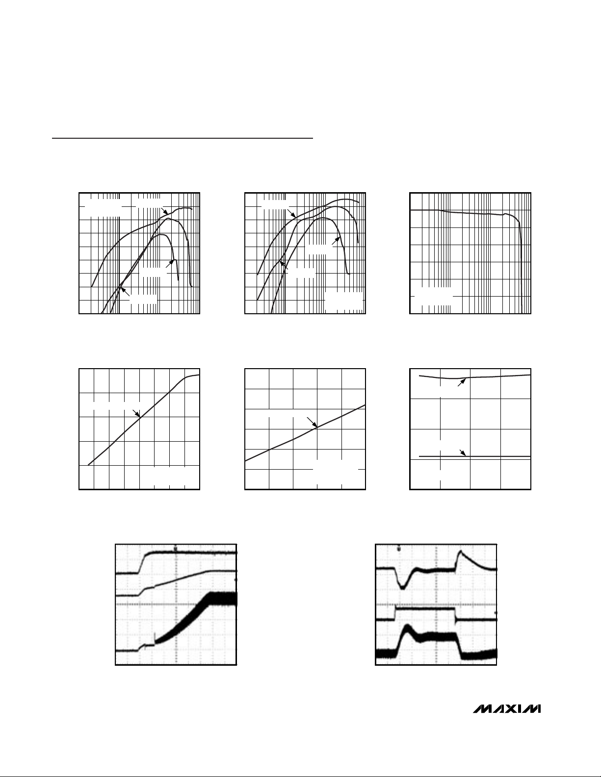
Typical Operating Characteristics
(Circuit of Figure 1, VIN= 3.3V, V
MAIN
= 8.5V, FREQ = SHDN = IN, TA= +25°C, unless otherwise noted.)
STEP-UP REGULATOR EFFICIENCY
vs. LOAD CURRENT (V
MAIN
= 8.5V)
MAX8758 toc01
LOAD CURRENT (mA)
EFFICIENCY (%)
10010
55
60
65
70
75
80
85
90
95
50
11000
f
OSC
= 1.2MHz
L = 4.7µH
VIN = 5.5V
VIN = 1.8V
VIN = 3.3V
STEP-UP REGULATOR EFFICIENCY
vs. LOAD CURRENT (V
MAIN
= 8.5V)
MAX8758 toc02
LOAD CURRENT (mA)
EFFICIENCY (%)
10010
55
60
65
70
75
80
85
90
95
50
1 1000
f
OSC
= 640kHz
L = 10µH
VIN = 5.5V
VIN = 1.8V
VIN = 3.3V
OUTPUT VOLTAGE (V)
8.0
8.1
8.2
8.3
8.4
8.5
8.6
7.9
STEP-UP REGULATOR OUTPUT VOLTAGE
vs. LOAD CURRENT (V
MAIN
= 8.5V)
MAX8758 toc03
LOAD CURRENT (mA)
100101 1000
f
OSC
= 1.2Hz
V
IN
= 3.3V
IN QUIESCENT CURRENT
vs. SUPPLY VOLTAGE
MAX8758 toc04
VIN (V)
SUPPLY CURRENT (µA)
5.04.54.03.53.02.52.0
10
20
30
40
50
0
1.5 5.5
CURRENT INTO IN PIN
NOT SWITCHING
V
FB
- 1.5V
TEMPERATURE (°C)
SUPPLY CURRENT (µA)
603510-15
25
26
27
28
29
30
24
-40 85
IN QUIESCENT CURRENT
vs. TEMPERATURE
MAX8758 toc05
CURRENT INTO IN PIN
VIN = 3.3V
NOT SWITCHING
V
FB
- 1.5V
SWITCHING FREQUENCY
vs. INPUT VOLTAGE
MAX8758 toc06
VIN (V)
SWITCHING FREQUENCY (kHz)
4.53.52.5
600
800
1000
1200
400
1.5 5.5
FREQ = V
IN
FREQ = AGND
I
MAIN
= 200mA
STEP-UP REGULATOR HEAVY-LOAD
SOFT-START
MAX8758 toc07
1ms
V
IN
2V/div
V
MAIN
5V/div
I
L
500mAV/div
STEP-UP REGULATOR LOAD TRANSIENT
RESPONSE
MAX8758 toc08
20µs/div
V
MAIN
AC-COUPLED
200mV/div
L = 4.7µH
R
COMP
= 100k
Ω
C
COMP1
= 220pF
C
COMP2
= 47pF
50mA
0
I
MAIN
500mA/div
I
L
1AV/div
Page 7

MAX8758
Step-Up Regulator with Switch Control and
Operational Amplifier for TFT LCD
_______________________________________________________________________________________ 7
STEP-UP REGULATOR PULSED LOAD
TRANSIENT RESPONSE
MAX8758 toc09
20µs/div
V
MAIN
AC-COUPLED
200mV/div
L = 4.7µH
R
COMP
= 100k
Ω
C
COMP1
= 220pF
C
COMP2
= 47pF
I
MAIN
1A/div
I
L
1AV/div
TIMER-DELAY LATCH RESPONSE
TO OVERLOAD
MAX8758 toc10
20ms/div
V
MAIN
5V/div
LX
5V/div
I
L
2A/div
0A
0V
0V
MAX8758 toc11
SUPB SUPPLY CURRENT
vs. SUPB VOLTAGE
V
SUPB
(V)
I
SUPB
(mA)
4.5 6.0 7.5 9.0 10.5 12.0 13.5 15.0
0.10
0.15
0.20
0.25
0.30
NO LOAD
BUFFER CONFIGURATION
POS_ = V
SUPB
/ 2
MAX8758 toc12
SUPB SUPPLY CURRENT
vs. TEMPERATURE
TEMPERATURE (°C)
I
SUPB
(mA)
-40 -10 20 50 70
0.10
0.15
0.20
0.25
0.30
NO LOAD
BUFFER CONFIGURATION
V
POSB
= V
SUPB
/ 2
V
SUPB
= 12V
V
SUPB
= 8V
V
SUPB
= 5V
OPERATIONAL AMPLIFIER FREQUENCY
RESPONSE FOR VARIOUS C
LOAD
MAX8758 toc13
FREQUENCY (Hz)
MAGNITUDE (dB)
10k1k
-40
-30
-20
-10
0
10
-50
100 100k
V
SUP
= 8.5V
A
V
= 1
R
L
= 10k
Ω
1000pF
56pF
POWER-SUPPLY REJECTION RATIO
vs. FREQUENCY
MAX8758 toc14
FREQUENCY (Hz)
PSRR (dB)
100k10k1k10010
20
40
60
80
100
120
0
11M
V
SUPB
= 8.5V
OP-AMP RAIL-TO-RAIL INPUT/OUTPUT
MAX8758 toc15
100µs/div
V
POSB
5V/div
V
OUTB
5V/div
OP-AMP LOAD TRANSIENT RESPONSE
MAX8758 toc16
1µs/div
I
OUTB
50mA/div
0
V
OUTB
2V/div
Typical Operating Characteristics (continued)
(Circuit of Figure 1, VIN= 3.3V, V
MAIN
= 8.5V, FREQ = SHDN = IN, TA= +25°C, unless otherwise noted.)
Page 8

MAX8758
Step-Up Regulator with Switch Control and
Operational Amplifier for TFT LCD
8 _______________________________________________________________________________________
Typical Operating Characteristics (continued)
(Circuit of Figure 1, VIN= 3.3V, V
MAIN
= 8.5V, FREQ = SHDN = IN, TA= +25°C, unless otherwise noted.)
OP-AMP LARGE-SIGNAL STEP RESPONSE
MAX8758 toc17
1µs/div
V
OUTB
2V/div
OP-AMP SMALL-SIGNAL STEP RESPONSE
MAX8758 toc18
200ns/div
V
POSB
100mV/div
AC-COUPLED
V
OUTB
200mV/div
AC-COUPLED
HIGH-VOLTAGE SWITCH CONTROL FUNCTION
(MODE 1)
MAX8758 toc19
400µs/div
V
MODE
V
CTL
V
GON
HIGH-VOLTAGE SWITCH CONTROL FUNCTION
(MODE 2)
MAX8758 toc20
400µs/div
V
MODE
V
CTL
V
GON
POSITIVE CHARGE-PUMP OUTPUT VOLTAGE
vs. CHARGE-PUMP LOAD CURRENT
MAX8758 toc21
CHARGE-PUMP LOAD CURRENT (mA)
OUTPUT VOLTAGE (V)
15105
21
22
23
24
25
20
020
VIN = 3.3V
f
OSC
= 1.2MHz
-9
-8
-7
-6
-5
-10
NEGATIVE CHARGE-PUMP OUTPUT VOLTAGE
vs. LOAD CURRENT
MAX8758 toc22
CHARGE-PUMP LOAD CURRENT (mA)
OUTPUT VOLTAGE (V)
15105020
VIN = 3.3V
f
OSC
= 1.2MHz
Page 9

MAX8758
Step-Up Regulator with Switch Control and
Operational Amplifier for TFT LCD
_______________________________________________________________________________________ 9
Pin Description
PIN NAME FUNCTION
1 GND Analog Ground
2 GON
Internal High-Voltage-Switch Common Connection. GON is the output of the high-voltage-switchcontrol block. GON is internally pulled to PGND through a 1kΩ resistor in shutdown. See the High-
Voltage Switch Control section for details.
3 CTL H i g h- V ol tag e, S w i tch- C ontr ol Bl ock Ti m i ng P i n. S ee the H i g h- V ol tag e S w i tch C ontr ol secti on for d etai l s.
4 DLP
High-Voltage, Switch-Control Block Delay Pin. Connect a capacitor from DLP to GND to set the delay
time. A 5µA current source charges C
DLP
. DLP is internally pulled to GND by a resistor in shutdown.
See the High-Voltage Switch Control section for details.
5 THR
GON Falling Regulation Adjustment Pin. Connect THR to the center of a resistive voltage-divider
between LDO or OUT and GND to adjust the V
GON
falling regulation level. The actual regulation level
is 10 x V
THR
. See the High-Voltage Switch Control section for details.
6 SUPB Operational Amplifier Supply Input. Bypass SUPB to GND with a 0.1µF capacitor.
7OUTB Operational Amplifier Output
8 NEGB Operational Amplifier Inverting Input
9 POSB Operational Amplifier Noninverting Input
10 N.C. No Connection. Not internally connected.
11 LDO
5V Internal Linear Regulator Output. This regulator powers all internal circuitry except the operational
amplifier. Bypass LDO to GND with a 0.22µF or greater ceramic capacitor.
12 OUT
Internal Linear Regulator Supply Pin. OUT is the supply input of the internal 5V linear regulator.
Connect OUT directly to the output of the step-up regulator.
13 I.C. Internally Connected. Make no connection to this pin.
14 SS
Soft-Start Control Pin. Connect a capacitor between SS and GND to set the soft-start period of the
step-up regulator. See the Bootstrapping and Soft-Start section for details.
15 COMP
Error Amplifier Compensation Pin. See the Step-Up Regulator Loop Compensation section for details.
16 FREQ
Frequency-Select Pin. Connect FREQ to GND for 600kHz operation, and connect FREQ to IN for
1.2MHz operation.
17 IN
Supply Pin. Bypass IN to GND with a 1µF ceramic capacitor. Place the capacitor close to the IN pin.
18 LX
Switching Node. LX is the drain of the internal power MOSFET. Connect the inductor and the Schottky
diode to LX and minimize trace area for low EMI.
19 SHDN
Shutdown Control Pin. Pull SHDN low to turn off the step-up regulator, the operational amplifier, and
the switch control block.
20 FB
Feedback Pin. The FB regulation point is 1.24V (typ). Connect FB to the center of a resistive voltagedivider between the step-up regulator output and GND to set the step-up regulator output voltage.
Place the divider close to the FB pin.
21 PGND Power Ground
22 MODE
High-Voltage, Switch-Control Block-Mode Selection Timing-Adjustment Pin. See the High-Voltage
Switch Control section for details. MODE is high impedance when it is connected to LDO. MODE is
internally pulled down by a 1kΩ resistor during UVLO, when V
DLP
< 0.5 x V
LDO
, or in shutdown.
23 DRN
High-Voltage, Switch-Control Input. DRN is the drain of the internal high-voltage p-channel MOSFET
connected to GON.
24 SRC
High-Voltage Switch-Control Input. SRC is the source of the internal high-voltage p-channel MOSFET.
Page 10

MAX8758
Typical Operating Circuit
The typical operating circuit (Figure 1) of the MAX8758
is a power-supply solution for TFT LCD panels in notebook computers. The circuit generates a +8.5V source
driver supply, and approximately +22V and -7V gate
driver supplies. The input voltage range for the IC is
from +1.8V to +5.5V, but the Figure 1 circuit is
designed to run from 2.7V to 3.6V. Table 1 lists some
selected components and Table 2 lists the contact
information of component suppliers.
Step-Up Regulator with Switch Control and
Operational Amplifier for TFT LCD
10 ______________________________________________________________________________________
MAX8758
V
MAIN
+8.5V/300mA
TO VCOM
BACKPLANE
V
GON
+24V/20mA
FROM TCON
V
IN
+1.8V TO +5.5V
V
GOFF
-8V/20mA
IN
FREQ
SHDN
COMP
LDO
FB
LX
GND
PGND
OUT
SUPB
GON
DRN
CTL
MODE
SS
POSB
NEGB
OUTB
THR
DLP
SRC
C15
0.1µF
C1
3.3µF
6.3V
C2
3.3µF
6.3V
R4
10Ω
C6
1µF
R10
100kΩ
R3
100kΩ
C7
220pF
C8
33pF
C9
0.22µF
C10
0.022µF
C11
150pF
R9
20kΩ
D2 D3
D4
C3
4.7µF
10V
C4
4.7µF
10V
C5
4.7µF
10V
L1
4.7µH
C6
0.1µF
C17
0.1µF
C19
0.1µF
C18
0.1µF
R1
200kΩ
1%
R2
34.0kΩ
1%
C12
0.1µF
R5
100kΩ
R6
100kΩ
R8
20.0kΩ
1%
R7
51.1kΩ
1%
C13
0.033µF
C14
0.1µF
D1
Figure 1. Typical Operating Circuit
Page 11

Detailed Description
The MAX8758 is designed primarily for TFT LCD panels
used in notebook computers. It contains a high-performance step-up regulator, a high-speed operational
amplifier, a logic-controlled, high-voltage switch-control
block with programmable delay, and an internal linear
regulator for bootstrapping operation. Figure 2 shows
the MAX8758 functional block diagram.
Step-Up Regulator
The step-up regulator is designed to generate the LCD
source driver supply. It employs a current-mode, fixedfrequency PWM architecture to maximize loop bandwidth and provide fast transient response to pulsed
loads typical of TFT LCD panel source drivers. The internal oscillator offers two pin-selectable frequency options
(640kHz/1.2MHz), allowing users to optimize their
designs based on the specific application requirements.
MAX8758
Step-Up Regulator with Switch Control and
Operational Amplifier for TFT LCD
______________________________________________________________________________________ 11
SRC
GON
DLP
MODE
THR
CTL
DRN
SWITCH
CONTROL
SUPB
NEGB
OUTB
POSB
GND
PGND
STEP-UP
REGULATOR
CONTROLLER
FB
COMP
SS
LX
LINEAR
REGULATOR
AND BOOTSTRAP
V
IN
MAX8758
SHDN
FREQ
LDO
IN
Figure 2. Functional Diagram
Table 1. Component List
DESIGNATION
DESCRIPTION
C1, C2
3.3µF ±10%, 6.3V X5R ceramic capacitors
(0603)
TDK C1608X5R0J335M
C3, C4, C5
4.7µF ±20%, 10V X5R ceramic capacitors
(1206)
TDK C3216X5R1A475M
D1
3A, 30V Schottky diode (M-flat)
Toshiba CMS02 (top mark S2)
D2, D3, D4
200mA, 100V dual diodes (SOT23)
Fairchild MMBD4148SE (top mark D4)
L1
4.2µH, 1.9A inductor
Sumida CDRH6D12-4R2
Page 12

MAX8758
The internal n-channel power MOSFET reduces the
number of external components. The supply rail of the
internal gate driver is bootstrapped to the internal linear
regulator output to improve the efficiency at low-input
voltages. The external-capacitor, soft-start function
effectively controls inrush currents. The output voltage
can be set from VINto 13V with an external resistive
voltage-divider.
PWM Control Block
Figure 3 is the block diagram of the step-up regulator.
The regulator controls the output voltage and the power
delivered to the output by modulating the duty cycle (D)
of the internal power MOSFET in each switching cycle.
The duty cycle of the MOSFET is approximated by:
where V
OUT
is the output voltage of the step-up regulator.
On the rising edge of the internal oscillator clock, the
controller sets a flip-flop, turning on the n-channel
MOSFET and applying the input voltage across the
inductor. The current through the inductor ramps up linearly, storing energy in its magnetic field. A transconductance error amplifier compares the FB voltage with
a 1.24V (typ) reference voltage. The error amplifier
changes the COMP voltage by charging or discharging
the COMP capacitor. The COMP voltage is compared
with a ramp, which is the sum of the current-sense signal and a slope compensation signal. Once the ramp
signal exceeds the COMP voltage, the controller resets
the flip-flop and turns off the MOSFET. Since the inductor current is continuous, a transverse potential develops across the inductor that turns on the Schottky
diode (D1 in Figure 1). The voltage across the inductor
then becomes the difference between the output voltage and the input voltage. This discharge condition
forces the current through the inductor to ramp down,
transferring the energy stored in the magnetic field to
the output capacitor and the load. The MOSFET
remains off for the rest of the clock cycle.
Bootstrapping and Soft-Start
The MAX8758 features bootstrapping operation. In normal operation, the internal linear regulator supplies
power to the internal circuitry. The input of the linear
regulator (OUT) should be directly connected to the
output of the step-up regulator. The step-up regulator is
enabled when the input voltage at OUT is above 1.75V,
SHDN is high, and the fault latch is not set.
After being enabled, the regulator starts open-loop
switching to generate the supply voltage for the linear
regulator with a controlled duty cycle. The internal reference block turns on when the LDO voltage exceeds
2.7V (typ). When the reference voltage reaches regulation, the PWM controller and the current-limit circuit are
enabled and the step-up regulator enters soft-start.
D
VV
V
OUT IN
OUT
≈
−
Step-Up Regulator with Switch Control and
Operational Amplifier for TFT LCD
12 ______________________________________________________________________________________
Table 2. Component Suppliers
SUPPLIER PHONE FAX WEBSITE
Fairchild Semiconductor 408-822-2000 408-822-2102 www.fairchildsemi.com
Sumida 847-545-6700 847-545-6720 www.sumida.com
TDK 847-803-6100 847-390-4405 www.component.tdk.com
Toshiba 949-455-2000 949-859-3963 www.toshiba.com/taec
Figure 3. Step-Up Regulator Block Diagram
CLOCK
OSCILLATOR
SLOPE COMP
TO FAULT LOGIC
LOGIC AND
DRIVER
ILIM
COMPARATOR
SOFTSTART
PWM
COMPARATOR
FAULT
COMPARATOR
∑
1.0V
I
LIMIT
CURRENT
SENSE
ERROR AMP
LX
PGND
SS
FB
1.24V
COMP
FREQ
Page 13

The soft-start timing can be adjusted with an external
capacitor connected between SS and GND. After the
step-up regulator is enabled, the SS pin is immediately
charged to 0.5V. Then the capacitor is charged at a
constant current of 4µA (typ). During this time, the SS
voltage directly controls the peak inductor current,
allowing a linear ramp from zero up to the full current
limit. The maximum load current is available after the
voltage on SS exceeds 1.5V. The soft-start capacitor is
discharged to ground when SHDN is low. The soft-start
routine minimizes inrush current and voltage overshoot
and ensures a well-defined startup behavior (see the
Step-Up Regulator Heavy Load Soft-Start waveform in
the Typical Operating Characteristics).
Fault Protection
During steady-state operation, the MAX8758 monitors the
FB voltage. If the FB voltage is below 1V (typ), the
MAX8758 activates an internal fault timer. If there is a
continuous fault for the fault-timer duration, the MAX8758
sets the fault latch, shutting down all the outputs. Once
the fault condition is removed, cycle the input voltage to
clear the fault latch and reactivate the device. The faultdetection circuit is disabled during the soft-start time.
The MAX8758 monitors the OUT voltage for undervoltage
and overvoltage conditions. If the OUT voltage is below
1.4V (typ) or above 13.5V (typ), the MAX8758 disables
the gate driver of the step-up regulator and prevents the
internal MOSFET from switching. The OUT undervoltage
and overvoltage conditions do not set the fault latch.
Thermal-Overload Protection
The thermal-overload protection prevents excessive
power dissipation from overheating the MAX8758.
When the junction temperature exceeds TJ= +160°C, a
thermal sensor immediately activates the fault protection, which sets the fault latch and shuts down all the
outputs, allowing the device to cool down. Once the
device cools down by approximately 15°C, cycle the
input voltage or toggle SHDN to clear the fault latch
and restart the device.
The thermal-overload protection protects the controller
in the event of fault conditions. For continuous operation, do not exceed the absolute maximum junction
temperature rating of TJ= +150°C.
Frequency Selection (FREQ)
The FREQ pin selects the switching frequency. Table 3
shows the switching frequency based on the FREQ connection. High-frequency (1.2MHz) operation optimizes
the application for the smallest component size, trading
off efficiency due to higher switching losses. Low-frequency (600kHz) operation offers the best overall efficiency at the expense of component size and board space.
Operational Amplifier
The MAX8758’s operational amplifier is typically used
to drive the LCD backplane (VCOM) or the gamma-correction-divider string. The operational amplifier features
±150mA output short-circuit current, 7.5V/µs slew rate,
and 12MHz bandwidth. The rail-to-rail input and output
capability maximizes system flexibility.
Short-Circuit Current Limit
The operational amplifier limits short-circuit current to
approximately ±150mA if the output is directly shorted to
SUPB or to GND. If the short-circuit condition persists,
the junction temperature of the IC rises until it reaches
the thermal shutdown threshold (+160°C typ). Once the
junction temperature reaches the thermal shutdown
threshold, an internal thermal sensor immediately sets
the thermal fault latch, shutting off all the IC’s outputs.
The device remains inactive until the input voltage is
cycled or SHDN is toggled.
Driving Pure Capacitive Load
The operational amplifier is typically used to drive the
LCD backplane (VCOM) or the gamma-correction
divider string. The LCD backplane consists of a distributed series capacitance and resistance, a load that can
be easily driven by the operational amplifier. However,
if the operational amplifier is used in an application with
a pure capacitive load, steps must be taken to ensure
stable operation.
As the operational amplifier’s capacitive load increases,
the amplifier’s bandwidth decreases and gain peaking
increases. A 5Ω to 50Ω small resistor placed between
OUTB and the capacitive load reduces peaking but also
reduces the gain. An alternative method of reducing
peaking is to place a series RC network (snubber) in parallel with the capacitive load. The RC network does not
continuously load the output or reduce the gain. Typical
values of the resistor are between 100Ω and 200Ω and
the typical value of the capacitor is 10pF.
High-Voltage Switch Control
The MAX8758’s high-voltage switch-control block (Figure
5) consists of two high-voltage, p-channel MOSFETs: Q1,
between SRC and GON and Q2, between GON and
DRN. The switch-control block is enabled when V
DLP
exceeds V
LDO
/2 and then Q1 and Q2 are controlled by
CTL and MODE. There are two different modes of operation (see the Typical Operating Characteristics section.)
MAX8758
Step-Up Regulator with Switch Control and
Operational Amplifier for TFT LCD
______________________________________________________________________________________ 13
Table 3. Frequency Selection
FREQ SWITCHING FREQUENCY (kHz)
GND 600
IN 1200
Page 14

MAX8758
Activate the first mode by connecting MODE to LDO.
When CTL is logic high, Q1 turns on and Q2 turns off,
connecting GON to SRC. When CTL is logic low, Q1
turns off and Q2 turns on, connecting GON to DRN.
GON can then be discharged through a resistor connected between DRN and PGND or AVDD. Q2 turns off
and stops discharging GON when V
GON
reaches 10
times the voltage on THR.
When V
MODE
is less than 0.9 x V
LDO
, the switch control
block works in the second mode. The rising edge of
V
CTL
turns on Q1 and turns off Q2, connecting GON to
SRC. An internal n-channel MOSFET Q3 between
MODE and GND is also turned on to discharge an
external capacitor between MODE and GND. The
falling edge of V
CTL
turns off Q3, and an internal 50µA
current source starts charging the MODE capacitor.
Once V
MODE
exceeds 0.5 x V
REF
, the switch control
block turns off Q1 and turns on Q2, connecting GON to
DRN. GON can then be discharged through a resistor
connected between DRN and GND or AVDD. Q2 turns
off and stops discharging GON when V
GON
reaches 10
times the voltage on THR.
The timing of enabling the switch control block can be
adjusted with an external capacitor connected between
DLP and GND. An internal current source starts charging the DLP capacitor if the input voltage is above
1.75V (typ), SHDN is high, and the fault latch is not set.
The voltage on DLP linearly rises because of the constant-charging current. When VDLP goes above 2.5V
(typ), the switch control block is enabled. The switch
control block is disabled and DLP is held low when the
MAX8758 is shut down or in a fault state.
Linear Regulator (LDO)
The MAX8758 includes an internal 5V linear regulator.
OUT is the input of the linear regulator and should be
directly connected to the output of the step-up regulator.
The input voltage range is between 4.5V and 13V. The
output of the linear regulator (LDO) is set to 5V (typ). The
regulator powers all the internal circuitry including the
gate driver. This feature significantly improves the efficiency at low input voltages. Bypass the LDO pin to
GND with a 0.22µF or greater ceramic capacitor.
Design Procedure
Step-Up Regulator
Step-Up Regulator Inductor Selection
The inductance value, peak-current rating, and series
resistance are factors to consider when selecting the
inductor. These factors influence the converter’s efficiency, maximum output-load capability, transient
response time, and output voltage ripple. Physical size
and cost are also important factors to be considered.
The maximum output current, input voltage, output voltage, and switching frequency determine the inductor
value. Very high inductance values minimize the current ripple and, therefore, reduce the peak current,
which decreases core losses in the inductor and I2R
losses in the entire power path. However, large inductor values also require more energy storage and more
turns of wire, which increase physical size and can
increase I2R losses in the inductor. Low inductance values decrease the physical size but increase the current
ripple and peak current. Finding the best inductor
involves choosing the best compromise between circuit
efficiency, inductor size, and cost.
The equations used here include a constant LIR, which
is the ratio of the inductor peak-to-peak ripple current
to the average DC inductor current at the full-load current. The best trade-off between inductor size and circuit efficiency for step-up regulators generally has an
LIR between 0.3 and 0.5. However, depending on the
AC characteristics of the inductor core material and
ratio of inductor resistance to other power-path resistances, the best LIR can shift up or down. If the inductor resistance is relatively high, more ripple can be
accepted to reduce the number of turns required and
increase the wire diameter. If the inductor resistance is
relatively low, increasing inductance to lower the peak
current can decrease losses throughout the power
path. If extremely thin high-resistance inductors are
used, as is common for LCD panel applications, the
best LIR can increase to between 0.5 and 1.0.
Step-Up Regulator with Switch Control and
Operational Amplifier for TFT LCD
14 ______________________________________________________________________________________
Page 15

MAX8758
Step-Up Regulator with Switch Control and
Operational Amplifier for TFT LCD
______________________________________________________________________________________ 15
REF
DLP
MODE
CTL
FAULT
SHDN
REF_OK
0.5 x V
REF
5µA
REF
50µA
1kΩ
9R
R
Q3
Q4
Q1
Q2
SRC
GON
DRN
THR
Q5
4R
1kΩ
5R
R
Figure 4. Switch Control
Page 16

MAX8758
In Figure 1’s Typical Operating Circuit, the LCD’s gate-
on and gate-off voltages are generated from two unregulated charge pumps driven by the step-up regulator’s
LX node. The additional load on LX must therefore be
considered in the inductance calculation. The effective
maximum output current I
MAIN(EFF)
becomes the sum
of the maximum load current on the step-up regulator’s
output plus the contributions from the positive and negative charge pumps:
I
MAIN(EFF)
= I
MAIN(MAX)
+ n
NEG
x I
NEG
+ (n
POS
+ 1) x I
POS
where I
MAIN(MAX)
is the maximum output current, n
NEG
is the number of negative charge-pump stages, n
POS
is
the number of positive charge-pump stages, I
NEG
is
the negative charge-pump output current, and I
POS
is
the positive charge-pump output current, assuming the
pump source for I
POS
is V
MAIN
.
The required inductance can then be calculated as
follows:
where VINis the typical input voltage and η
TYP
is the
expected efficiency obtained from the appropriate
curve in the Typical Operating Characteristics.
Choose an available inductor value from an appropriate
inductor family. Calculate the maximum DC input current at the minimum input voltage V
IN(MIN)
using con-
servation of energy and the expected efficiency at that
operating point (η
MIN
) taken from an appropriate curve
in the Typical Operating Characteristics:
Calculate the ripple current at that operating point and
the peak current required for the inductor:
The inductor’s saturation current rating and the guaranteed minimum value of the MAX8758’s LX current limit
(I
LIM
) should exceed I
PEAK
and the inductor’s DC current
rating should exceed I
IN(DC,MAX)
. For good efficiency,
choose an inductor with less than 0.1Ω series resistance.
Considering the Typical Operating Circuit, the maximum load current (I
MAIN(MAX)
) is 300mA for the stepup regulator, 20mA for the two-stage positive charge
pump, and 20mA for the one-stage negative charge
pump. Altogether, the effective maximum output current, I
MAIN(EFF)
is 360mA with an 8.5V output and a
typical input voltage of 3.3V. The switching frequency is
set to 1.2MHz. Choosing an LIR of 0.4 and estimating
efficiency of 85% at this operating point:
Using the circuit’s minimum input voltage (3V) and estimating efficiency of 80% at that operating point:
The ripple current and the peak current are:
The peak-inductor current does not exceed the guaranteed minimum value of the LX current limit in the
Electrical Characteristics table.
Step-Up Regulator Output Capacitor Selection
The total output voltage ripple has two components: the
capacitive ripple caused by the charging and discharging of the output capacitance, and the ohmic ripple due
to the capacitor’s equivalent series resistance (ESR):
V
RIPPLE
= V
RIPPLE(C)
+ V
ARIPPLE(ESR)
and
V
RIPPLE(ESR)
≈ I
PEAK
x R
ESR
where I
PEAK
is the peak inductor current (see the Step-
Up Regulator Inductor Selection section). For ceramic
capacitors, the output voltage ripple is typically dominated by V
RIPPLE(C)
. The voltage rating and temperature
characteristics of the output capacitor must also be considered.
V
I
C
VV
Vf
RIPPLE C
MAIN
MAIN
MAIN IN
MAIN SW
()
≈ ×
×
−
IAAA
PEAK
. . .=+≈128
04
2
148
I
VVV
HVMHz
A
RIPPLE
(. )
. . .
.=
×
××
≈
−3853
42 85 12
04
µ
I
AV
V
A
IN DC MAX(, )
. .
.
.=
×
×
≈
036 85
308
128
L
V
V
VV
A MHz
H
.
.
. .
. .
.
.
.=
×
−
×
×
≈
33
85
85 33
036 12
085
04
42
2
µ
II
I
PEAK IN DC MAX
RIPPLE
(, )
=+
2
I
VVV
LV f
RIPPLE
IN MIN MAIN IN MIN
MAIN OSC
() ()
=
×
()
××
−
I
IV
V
IN DCMAX
MAIN EFF MAIN
IN MIN MIN
(, )
()
()
=
×
× η
L
V
V
VV
IfLIR
IN
MAIN
MAIN IN
MAIN EFF OSC
TYP
()
=
×
×
×
−
2
η
Step-Up Regulator with Switch Control and
Operational Amplifier for TFT LCD
16 ______________________________________________________________________________________
Page 17

Step-Up Regulator Input Capacitor Selection
The input capacitor reduces the current peaks drawn
from the input supply and reduces noise injection into
the IC. Two 10µF ceramic capacitors are used in the
Typical Applications Circuit (Figure 1) because of the
high source impedance seen in typical lab setups.
Actual applications usually have much lower source
impedance since the step-up regulator often runs
directly from the output of another regulated supply.
Typically, the input capacitance can be reduced below
the values used in the Typical Applications Circuit.
Step-Up Regulator Rectifier Diode
The MAX8758’s high switching frequency demands a
high-speed rectifier. Schottky diodes are recommended for most applications because of their fast recovery
time and low forward voltage. In general, a 2A Schottky
diode complements the internal MOSFET well.
Step-Up Regulator Output Voltage Selection
The output voltage of the step-up regulator can be
adjusted by connecting a resistive voltage-divider from
the output (V
OUT
) to GND with the center tap connect-
ed to FB (see Figure 1). Select R2 in the 10kΩ to 50kΩ
range. Calculate R1 with the following equation:
where VFB, the step-up regulator’s feedback set point,
is 1.25V. Place R1 and R2 close to the IC.
Step-Up Regulator Loop Compensation
Choose R
COMP
(R3 in Figure 1) to set the high-frequency integrator gain for fast transient response. Choose
C
COMP
(C7 in Figure 1) to set the integrator zero to
maintain loop stability.
For low-ESR output capacitors, use the following equations to obtain stable performance and good transient
response:
To further optimize transient response, vary R
COMP
in
20% steps and C
COMP
in 50% steps while observing
transient-response waveforms.
Place C
COMP2
(C8 in Figure 1) from COMP to GND to
add an additional high-frequency pole. UseC
COMP2
between 10pF and 47pF.
Step-Up Regulator Soft-Start Capacitor
The soft-start capacitor should be large enough that it
does not reach final value before the output has
reached regulation. Calculate the soft-start capacitor
(CSS) value using:
where C
MAIN
is the total output capacitance, V
MAIN
is
the maximum output voltage, and I
INRUSH
is the peak
inrush current allowed, I
MAIN
is the maximum output
current, and VINis the minimum input voltage.
The load must wait for the soft-start cycle to finish
before drawing a significant amount of load current.
The duration after which the load can begin to draw
maximum load current is:
t
MAX
= 6.77 x 10⁵x C
SS
Charge Pumps
Selecting the Number of Charge-Pump Stages
For highest efficiency, always choose the lowest number of charge-pump stages that meet the output voltage requirement.
The number of positive charge-pump stages is given by:
where n
POS
is the number of positive-charge-pump
stages, V
GON
is the positive-charge-pump output,
V
MAIN
is the main step-up regulator output, and VDis
the forward voltage drop of the charge-pump diode.
The number of negative charge-pump stages is given by:
where n
NEG
is the number of negative-charge-pump
stages, V
GOFF
is the negative charge-pump output,
V
MAIN
is the main step-up regulator output, and VDis
the forward voltage drop of the charge-pump diode.
n
V
VV
NEG
GOFF
MAIN D
=×
−
−
2
n
VV
VV
POS
GON MAIN
MAIN D
=×
−
−
2
CC
VVV
VI I V
SS MAIN
MAIN
IN MAIN
IN INRUSH MAIN MAIN
=× ×
×
×
××
−
−
−
21 10
6
2
C
VC
IR
COMP
MAIN MAIN
MAIN MAX COMP
()
≈
×
××10
R
VV C
LI
COMP
IN MAIN MAIN
MAIN MAX
()
≈
×× ×
×
315
RR
V
V
MAIN
FB
12 1 =×
−
MAX8758
Step-Up Regulator with Switch Control and
Operational Amplifier for TFT LCD
______________________________________________________________________________________ 17
Page 18

MAX8758
Charge-Pump Flying Capacitors
Increasing the flying capacitor (C6, C17, C18) value
lowers the effective source impedance and increases
the output-current capability. Increasing the capacitance indefinitely has a negligible effect on output-current capability because the diode impedance places a
lower limit on the source impedance. Ceramic capacitors of 0.1µF or greater work well in most applications
that require output currents in the order of 10mA to
20mA.
The flying capacitor’s voltage rating must exceed the
following:
VC> n x V
MAIN
where n is the stage number in which the flying capacitor appears, and V
MAIN
is the output voltage of the
main step-up regulator.
Charge-Pump Output Capacitor
Increasing the output capacitance or decreasing the
ESR reduces the output voltage ripple and the peak-topeak voltage during load transients. With ceramic
capacitors, the output voltage ripple is dominated by
the capacitance value. Use the following equation to
approximate the required capacitor value:
where C
MAIN_CP
is the output capacitor of the charge
pump, I
LOAD_CP
is the load current of the charge
pump, and V
RIPPLE_CP
is the peak-to-peak value of the
output ripple.
The charge-pump output capacitor is typically also the
input capacitor for a linear regulator. Often, its value must
be increased to maintain the linear regulator’s stability.
Charge-Pump Rectifier Diodes
Use low-cost, silicon-switching diodes with a current
rating equal to or greater than two times the average
charge-pump input current. If it helps avoid an extra
stage, some or all of the diodes can be replaced with
Schottky diodes with equivalent current ratings.
PC Board Layout and Grounding
Careful PC board layout is important for proper operation.
Use the following guidelines for good PC board layout:
1) Minimize the area of high-current loops by placing
the step-up regulator’s inductor, diode, and output
capacitors near its input capacitors, its LX, and
PGND pin. The high-current input loop goes from
the positive terminal of the input capacitor to the
inductor, to the IC’s LX pin, out of PGND, and to
the input capacitor’s negative terminal. The highcurrent output loop is from the positive terminal of
the input capacitor to the inductor, to the output
diode (D1), to the positive terminal of the output
capacitors, reconnecting between the output
capacitor and input capacitor ground terminals.
Connect these loop components with short, wide
connections. Avoid using vias in the high-current
paths. If vias are unavoidable, use many vias in
parallel to reduce resistance and inductance.
2) Create a power ground island (PGND) for the
step-up regulator, consisting of the input and output capacitor grounds and the PGND pin.
Maximizing the width of the power ground traces
improves efficiency and reduces output voltage
ripple and noise spikes. Create an analog ground
plane (GND) consisting of the GND pin, the feedback-divider ground connection, the COMP and
DLP capacitor ground connections, and the
device’s exposed backside pad. Connect the
PGND and GND islands by connecting the two
ground pins directly to the exposed backside pad.
Make no other connections between these separate ground planes.
3) Place the feedback voltage-divider resistors as
close to the feedback pin as possible. The
divider’s center trace should be kept short.
Placing the resistors far away causes the FB trace
to become antennas that can pick up switching
noise. Care should be taken to avoid running the
feedback trace near LX.
4) Place the IN pin bypass capacitor as close to the
device as possible. The ground connection of the
IN bypass capacitor should be connected directly
to the GND pin with a wide trace.
5) Minimize the length and maximize the width of the
traces between the output capacitors and the load
for best transient responses.
6) Minimize the size of the LX node while keeping it
wide and short. Keep the LX node away from
feedback node (FB) and analog ground. Use DC
traces as shield if necessary.
Refer to the MAX8758 evaluation kit for an example of
proper board layout.
C
I
fV
MAIN CP
LOAD CP
OSC RIPPLE CP
_
_
_
≥
××2
Step-Up Regulator with Switch Control and
Operational Amplifier for TFT LCD
18 ______________________________________________________________________________________
Page 19

MAX8758
Step-Up Regulator with Switch Control and
Operational Amplifier for TFT LCD
______________________________________________________________________________________ 19
Chip Information
TRANSISTOR COUNT: 3208
PROCESS: BiCMOS
Pin Configuration
MAX8758
TOP VIEW
2
GON
1
GND
3
CTL
4
DLP5THR
6
SUPB
24
SRC
23
DRN
22
MODE
21
PGND
20
FB
19
SHDN
18LX17IN16
FREQ15COMP14SS13I.C.
11
LDO
10
N.C.
12
OUT
9
POSB
8
NEGB
7
OUTB
Page 20

MAX8758
Step-Up Regulator with Switch Control and
Operational Amplifier for TFT LCD
Maxim cannot assume responsibility for use of any circuitry other than circuitry entirely embodied in a Maxim product. No circuit patent licenses are
implied. Maxim reserves the right to change the circuitry and specifications without notice at any time.
20 ____________________Maxim Integrated Products, 120 San Gabriel Drive, Sunnyvale, CA 94086 408-737-7600
© 2005 Maxim Integrated Products Printed USA is a registered trademark of Maxim Integrated Products, Inc.
Package Information
(The package drawing(s) in this data sheet may not reflect the most current specifications. For the latest package outline information,
go to www.maxim-ic.com/packages
.)
QFN THIN.EPS
D2
(ND-1) X e
e
D
C
PIN # 1
I.D.
(NE-1) X e
E/2
E
0.08 C
0.10 C
A
A1
A3
DETAIL A
E2/2
E2
0.10 M C A B
PIN # 1 I.D.
b
0.35x45°
D/2
D2/2
L
C
L
C
e e
L
CC
L
k
LL
DETAIL B
L
L1
e
XXXXX
MARKING
H
1
2
21-0140
PACKAGE OUTLINE,
16, 20, 28, 32, 40L THIN QFN, 5x5x0.8mm
-DRAWING NOT TO SCALE-
L
e/2
COMMON DIMENSIONS
3.353.15T2855-1 3.25 3.353.15 3.25
MAX.
3.20
EXPOSED PAD VARIATIONS
3.00T2055-2 3.10
D2
NOM.MIN.
3.203.00 3.10
MIN.E2NOM. MAX.
NE
ND
PKG.
CODES
1. DIMENSIONING & TOLERANCING CONFORM TO ASME Y14.5M-1994.
2. ALL DIMENSIONS ARE IN MILLIMETERS. ANGLES ARE IN DEGREES.
3. N IS THE TOTAL NUMBER OF TERMINALS.
4. THE TERMINAL #1 IDENTIFIER AND TERMINAL NUMBERING CONVENTION SHALL
CONFORM TO JESD 95-1 SPP-012. DETAILS OF TERMINAL #1 IDENTIFIER ARE
OPTIONAL, BUT MUST BE LOCATED WITHIN THE ZONE INDICATED. THE TERMINAL #1
IDENTIFIER MAY BE EITHER A MOLD OR MARKED FEATURE.
5. DIMENSION b APPLIES TO METALLIZED TERMINAL AND IS MEASURED BETWEEN
0.25 mm AND 0.30 mm FROM TERMINAL TIP.
6. ND AND NE REFER TO THE NUMBER OF TERMINALS ON EACH D AND E SIDE RESPECTIVELY.
7. DEPOPULATION IS POSSIBLE IN A SYMMETRICAL FASHION.
8. COPLANARITY APPLIES TO THE EXPOSED HEAT SINK SLUG AS WELL AS THE TERMINALS.
9. DRAWING CONFORMS TO JEDEC MO220, EXCEPT EXPOSED PAD DIMENSION FOR T2855-1,
T2855-3, AND T2855-6.
NOTES:
SYMBOL
PKG.
N
L1
e
E
D
b
A3
A
A1
k
10. WARPAGE SHALL NOT EXCEED 0.10 mm.
JEDEC
T1655-1 3.203.00 3.10 3.00 3.10 3.20
0.70 0.800.75
4.90
4.90
0.25
0.250--
4
WHHB
4
16
0.350.30
5.10
5.105.00
0.80 BSC.
5.00
0.05
0.20 REF.
0.02
MIN. MAX.NOM.
16L 5x5
3.10
T3255-2
3.00
3.20
3.00 3.10 3.20
2.70
T2855-2 2.60 2.602.80 2.70 2.80
L
0.30 0.500.40
---
---
WHHC
20
5
5
5.00
5.00
0.30
0.55
0.65 BSC.
0.45
0.25
4.90
4.90
0.25
0.65
--
5.10
5.10
0.35
20L 5x5
0.20 REF.
0.75
0.02
NOM.
0
0.70
MIN.
0.05
0.80
MAX.
---
WHHD-1
28
7
7
5.00
5.00
0.25
0.55
0.50 BSC.
0.45
0.25
4.90
4.90
0.20
0.65
--
5.10
5.10
0.30
28L 5x5
0.20 REF.
0.75
0.02
NOM.
0
0.70
MIN.
0.05
0.80
MAX.
---
WHHD-2
32
8
8
5.00
5.00
0.40
0.50 BSC.
0.30
0.25
4.90
4.90
0.50
--
5.10
5.10
32L 5x5
0.20 REF.
0.75
0.02
NOM.
0
0.70
MIN.
0.05
0.80
MAX.
0.20 0.25 0.30
DOWN
BONDS
ALLOWED
NO
YES3.103.00 3.203.103.00 3.20T2055-3
3.103.00 3.203.103.00 3.20T2055-4
T2855-3 3.15 3.25 3.35 3.15 3.25 3.35
T2855-6 3.15 3.25 3.35 3.15 3.25 3.35
T2855-4 2.60 2.70 2.80 2.60 2.70 2.80
T2855-5 2.60 2.70 2.80 2.60 2.70 2.80
T2855-7 2.60 2.70
2.80
2.60 2.70 2.80
3.203.00 3.10T3255-3 3.203.00 3.10
3.203.00 3.10T3255-4 3.203.00 3.10
NO
NO
NO
NO
NO
NO
NO
NO
YES
YES
YES
YES
3.203.00T1655-2 3.10 3.00 3.10 3.20 YES
NO3.203.103.003.10T1655N-1 3.00 3.20
3.353.15T2055-5 3.25 3.15 3.25 3.35
YES
3.35
3.15T2855N-1 3.25 3.15 3.25 3.35
NO
3.35
3.15T2855-8 3.25 3.15 3.25 3.35
YES
3.203.10T3255N-1 3.00
NO
3.203.103.00
L
0.40
0.40
**
**
**
**
**
**
**
**
**
**
**
**
**
**
**
**
**
**
**
SEE COMMON DIMENSIONS TABLE
±0.15
11. MARKING IS FOR PACKAGE ORIENTATION REFERENCE ONLY.
H
2
2
21-0140
PACKAGE OUTLINE,
16, 20, 28, 32, 40L THIN QFN, 5x5x0.8mm
-DRAWING NOT TO SCALE-
12. NUMBER OF LEADS SHOWN ARE FOR REFERENCE ONLY.
3.30T4055-1 3.20 3.40 3.20 3.30 3.40
**
YES
0.0500.02
0.600.40 0.50
10
-----
0.30
40
10
0.40 0.50
5.10
4.90 5.00
0.25 0.35 0.45
0.40 BSC.
0.15
4.90
0.250.20
5.00 5.10
0.20 REF.
0.70
MIN.
0.75 0.80
NOM.
40L 5x5
MAX.
13. LEAD CENTERLINES TO BE AT TRUE POSITION AS DEFINED BY BASIC DIMENSION "e", ±0.05.
 Loading...