

Page 1
For pricing, delivery, and ordering information, please contact Maxim/Dallas Direct! at
1-888-629-4642, or visit Maxim’s website at www.maxim-ic.com.
General Description
The MAX8741/MAX8742 are buck-topology, step-down,
switch-mode, power-supply controllers that generate
logic-supply voltages in battery-powered systems. These
high-performance, dual/triple-output devices include onboard power-up sequencing, power-good signaling with
delay, digital soft-start, secondary winding control, lowdropout circuitry, internal frequency-compensation networks, and automatic bootstrapping.
Up to 97% efficiency is achieved through synchronous
rectification and Maxim’s proprietary Idle Mode™ control
scheme. Efficiency is greater than 80% over a 1000:1
load-current range, which extends battery life in system
suspend or standby mode. Excellent dynamic response
corrects output load transients within five clock cycles.
Strong 1A on-board gate drivers ensure fast external
n-channel MOSFET switching.
These devices feature a logic-controlled and synchronizable, fixed-frequency, pulse-width-modulation (PWM)
operating mode. This reduces noise and RF interference
in sensitive mobile communications and pen-entry applications. Asserting the SKIP pin enables fixed-frequency
mode, for lowest noise under all load conditions.
The MAX8741/MAX8742 include two PWM regulators,
adjustable from 2.5V to 5.5V with fixed 5.0V and 3.3V
modes. All these devices include secondary feedback
regulation, and the MAX8742 contains a 12V/120mA linear regulator. The MAX8741 includes a secondary feedback input (SECFB), plus a control pin (STEER) that
selects which PWM (3.3V or 5V) receives the secondary
feedback signal. SECFB provides a method for adjusting
the secondary winding voltage regulation point with an
external resistor-divider, and is intended to aid in creating
auxiliary voltages other than fixed 12V.
The MAX8741/MAX8742 contain internal output overvoltage- and undervoltage-protection features.
________________________Applications
Notebook and Subnotebook Computers
PDAs and Mobile Communicators
Desktop CPU Local DC-DC Converters
Features
♦ 97% Efficiency
♦ 4.2V to 30V Input Range
♦ 2.5V to 5.5V Dual Adjustable Outputs
♦ Selectable 3.3V and 5V Fixed or Adjustable
Outputs (Dual Mode™)
♦ 12V Linear Regulator
♦ Adjustable Secondary Feedback (MAX8741)
♦ 5V/50mA Linear-Regulator Output
♦ Precision 2.5V Reference Output
♦ Programmable Power-Up Sequencing
♦ Power-Good (RESET) Output
♦ Output Overvoltage Protection
♦ Output Undervoltage Shutdown
♦ 333kHz/500kHz Low-Noise, Fixed-Frequency
Operation
♦ Low-Dropout, 98% Duty-Factor Operation
♦ 2.5mW Typical Quiescent Power (12V Input,
Both SMPSs On)
♦ 4µA Typical Shutdown Current
MAX8741/MAX8742
500kHz Multi-Output Power-Supply Controllers
with High Impedance in Shutdown
________________________________________________________________ Maxim Integrated Products 1
5V
LINEAR
12V
LINEAR
POWER-UP
SEQUENCE
POWER-
GOOD
3.3V
SMPS
5V
SMPS
RESETON/OFF
5V (RTC)
3.3V
INPUT
5V
12V
Functional Diagram
19-3262; Rev 0; 4/04
Ordering Information
Idle Mode is a trademark of Maxim Integrated Products, Inc.
Dual Mode is a trademark of Maxim Integrated Products, Inc.
Pin Configurations appear at end of data sheet.
PART
TEMP RANGE
PIN-PACKAGE
MAX8741EAI
28 SSOP
MAX8741ETJ
32 Thin QFN 5m m x 5m m
MAX8742EAI
28 SSOP
MAX8742ETJ
32 Thin QFN 5m m x 5m m
-40°C to +85°C
-40°C to +85°C
-40°C to +85°C
-40°C to +85°C
Page 2
MAX8741/MAX8742
500kHz Multi-Output Power-Supply Controllers
with High Impedance in Shutdown
2 _______________________________________________________________________________________
ABSOLUTE MAXIMUM RATINGS
ELECTRICAL CHARACTERISTICS
(V+ = 15V, both PWMs on, SYNC = VL, VLload = 0, REF load = 0, SKIP = 0, TA= 0°C to +85°C, unless otherwise noted. Typical
values are at T
A
= +25°C.)
Stresses beyond those listed under “Absolute Maximum Ratings” may cause permanent damage to the device. These are stress ratings only, and functional
operation of the device at these or any other conditions beyond those indicated in the operational sections of the specifications is not implied. Exposure to
absolute maximum rating conditions for extended periods may affect device reliability.
V+ to GND..............................................................-0.3V to +36V
PGND to GND.....................................................................±0.3V
V
L
to GND ................................................................-0.3V to +6V
BST3, BST5 to GND ..............................................-0.3V to +36V
CSH3, CSH5 to GND................................................-0.3V to +6V
FB3 to GND..............................................-0.3V to (CSL3 + 0.3V)
FB5 to GND...............................................-0.3V to (CSL5 +0.3V)
LX3 to BST3..............................................................-6V to +0.3V
LX5 to BST5..............................................................-6V to +0.3V
REF, SYNC, SEQ, STEER, SKIP,
TIME/ON5, SECFB, RESET to GND ..........-0.3V to (V
L
+ 0.3V)
V
DD
to GND............................................................-0.3V to +20V
RUN/ON3, SHDN to GND.............................-0.3V to (V+ + 0.3V)
12OUT to GND ..........................................-0.3V to (V
DD
+ 0.3V)
DL3, DL5 to PGND........................................-0.3V to (V
L
+ 0.3V)
DH3 to LX3 ..............................................-0.3V to (BST3 + 0.3V)
DH5 to LX5 ..............................................-0.3V to (BST5 + 0.3V)
V
L
, REF Short to GND ................................................Momentary
12OUT Short to GND..................................................Continuous
REF Current...........................................................+5mA to -1mA
V
L
Current.........................................................................+50mA
12OUT Current . .............................................................+200mA
V
DD
Shunt Current............................................................+15mA
Continuous Power Dissipation (T
A
= +70°C)
28-Pin SSOP (derate 9.52mW/°C above +70°C) ........762mW
32-Pin Thin QFN (derate 21.3mW/°C above +70°C) ....1702mW
Operating Temperature Range ...........................-40°C to +85°C
Storage Temperature Range ............................-65°C to +160°C
Lead Temperature (soldering, 10s) ................................+300°C
PARAMETER CONDITIONS
UNITS
MAIN SMPS CONTROLLERS
Input Voltage Range 4.2
V
3V Output Voltage in Adjustable Mode
V+ = 4.2V to 30V, CSH3 - CSL3 = 0,
CSL3 connected to FB3
2.5
V
3V Output Voltage in Fixed Mode
V+ = 4.2V to 30V, 0 < CSH3 - CSL3
< 80mV, FB3 = 0
V
5V Output Voltage in Adjustable Mode
V+ = 4.2V to 30V, CSH5 - CSL5 = 0,
CSL5 connected to FB5
2.5
V
5V Output Voltage in Fixed Mode
V+ = 5.3V to 30V, 0 < CSH5 - CSL5
< 80mV, FB5 = 0
V
Output Voltage Adjust Range Either SMPS
5.5 V
Adjustable-Mode Threshold Voltage Dual-mode comparator 0.5 1.1 V
Load Regulation Either SMPS, 0 < CSH_ - CSL_ < 80mV -2 %
Line Regulation Either SMPS, 5.2V < V+ < 30V
%/V
CSH3 - CSL3 or CSH5 - CSL5 80 100
Current-Limit Threshold
SKIP = V
L
or VDD < 13V or SECFB < 2.44V -50
mV
Idle-Mode Threshold SKIP = 0, not tested 10 25 40 mV
Soft-Start Ramp Time
From enable to 95% full current limit with
respect to f
OSC
(Note 1)
512
Clks
SYNC = V
L
500
Oscillator Frequency
SYNC = 0
333
kHz
MIN TYP MAX
2.42
3.20 3.39 3.47
2.42
4.85 5.13 5.25
REF
0.03
450
283
-100 -150
30.0
2.58
2.58
120
550
383
Page 3
MAX8741/MAX8742
500kHz Multi-Output Power-Supply Controllers
with High Impedance in Shutdown
_______________________________________________________________________________________ 3
ELECTRICAL CHARACTERISTICS (continued)
(V+ = 15V, both PWMs on, SYNC = VL, VLload = 0, REF load = 0, SKIP = 0, TA= 0°C to +85°C, unless otherwise noted. Typical
values are at T
A
= +25°C.)
PARAMETER CONDITIONS
MIN
TYP
MAX
UNITS
SYNC = V
L
95 97
Maximum Duty Factor
SYNC = 0 (Note 2)
98
%
SYNC Input High Pulse Width Not tested
ns
SYNC Input Low Pulse Width Not tested
ns
SYNC Rise/Fall Time Not tested
ns
SYNC Input-Frequency Range
kHz
Current-Sense Input Leakage Current
V+ = V
L
= 0,
CSL3 = CSH3 = CSL5 = CSH5 = 5.5V
10 µA
FLYBACK CONTROLLER
VDD Regulation Threshold Falling edge (MAX8742) 13 14 V
SECFB Regulation Threshold Falling edge (MAX8741)
V
DL Pulse Width VDD < 13V or SECFB < 2.44V
µs
VDD Shunt Threshold Rising edge, hysteresis = 1% (MAX8742) 18 20 V
VDD Shunt Sink Current V
DD
= 20V (MAX8742) 10 mA
VDD Leakage Current V
DD
= 5V, off mode (Note 3) 30 µA
12V LINEAR REGULATOR (MAX8742)
12OUT Output Voltage 13V < V
DD
< 18V, 0 < I
LOAD
< 120mA
V
12OUT Current Limit 12OUT forced to 11V, V
DD
= 13V 150 mA
Quiescent V
DD
Current V
DD
= 18V, run mode, no 12OUT load 50
µA
INTERNAL REGULATOR AND REFERENCE
VL Output Voltage
SHDN = V+, RUN/ON3 = TIME/ON5 = 0,
5.4V < V+ < 30V, 0mA < I
LOAD
< 50mA
4.7 5.1 V
VL Undervoltage-Lockout Fault Threshold Falling edge, hysteresis = 1% 3.5 3.6 3.7 V
VL Switchover Threshold Rising edge of CSL5, hysteresis = 1% 4.2 4.5 4.7 V
REF Output Voltage No external load (Note 4)
2.5
V
0 < I
LOAD
< 50µA
REF Load Regulation
0 < I
LOAD
< 5mA
mV
REF Sink Current 10 µA
REF Fault-Lockout Voltage Falling edge 1.8 2.4 V
V+ Operating Supply Current VL switched over to CSL5, 5V SMPS on 5 50 µA
V+ Standby Supply Current
V+ = 5.5V to 30V, both SMPSs off, includes
current into SHDN
30 60 µA
V+ Standby Supply Current in Dropout
V+ = 4.2V to 5.5V, both SMPSs off, includes
current into SHDN
50
µA
V+ Shutdown Supply Current V+ = 4.0V to 30V, SHDN = 0 4 10 µA
MAX8742 2.5 4
Quiescent Power Consumption
Both SMPSs enabled,
FB3 = FB5 = 0,
CSL3 = CSH3 = 3.5V,
CSL5 = CSH5 = 5.3V
MAX8741 1.5 4
mW
96.5
200
200
400 583
0.01
2.44 2.60
0.75
11.65 12.10 12.50
2.45
200
100
2.55
12.5
100.0
200
Page 4
MAX8741/MAX8742
500kHz Multi-Output Power-Supply Controllers
with High Impedance in Shutdown
4 _______________________________________________________________________________________
ELECTRICAL CHARACTERISTICS (continued)
(V+ = 15V, both PWMs on, SYNC = VL, VLload = 0, REF load = 0, SKIP = 0, TA= 0°C to +85°C, unless otherwise noted. Typical
values are at T
A
= +25°C.)
PARAMETER CONDITIONS
MIN
TYP
MAX
UNITS
FAULT DETECTION
Overvoltage Trip Threshold With respect to unloaded output voltage 4 7 10 %
Overvoltage Fault Propagation Delay
CSL_ driven 2% above overvoltage trip
threshold
1.5 µs
Output Undervoltage Threshold With respect to unloaded output voltage 60 70 80 %
Output Undervoltage-Lockout Time
From each SMPS enabled, with respect to
f
OSC
Clks
Thermal-Shutdown Threshold Typical hysteresis = 10°C
°C
RESET
RESET Trip Threshold
With respect to unloaded output voltage,
falling edge; typical hysteresis = 1%
-7
-4 %
RESET Propagation Delay
Falling edge, CSL_ driven 2% below RESET
trip threshold
1.5 µs
RESET Delay Time With respect to f
OSC
Clks
INPUTS AND OUTPUTS
Feedback-Input Leakage Current FB3, FB5; SECFB = 2.6V 1 50 nA
Logic Input-Low Voltage
RUN/ON3, SKIP, TIME/ON5 (SEQ = REF),
SHDN, STEER, SYNC
0.6 V
Logic Input-High Voltage
RUN/ON3, SKIP, TIME/ON5 (SEQ = REF),
SHDN, STEER, SYNC
2.4 V
Input Leakage Current
RUN/ON3, SKIP, TIME/ON5 (SEQ = REF),
±1µA
Logic Output-Low Voltage RESET, I
SINK
= 4mA 0.4 V
Logic Output-High Current RESET = 3.5V 1 mA
TIME/ON5 Input Trip Level SEQ = 0 or V
L
2.4 2.6 V
TIME/ON5 Source Current TIME/ON5 = 0, SEQ = 0 or V
L
2.5 3 3.5 µA
TIME/ON5 On-Resistance TIME/ON5; RUN/ON3 = 0, SEQ = 0 or V
L
15 80 Ω
Gate-Driver Sink/Source Current DL3, DH3, DL5, DH5; forced to 2V 1 A
SSOP package 1.5 7
Gate-Driver On-Resistance
QFN package 1.5 8
Ω
3300 4096 4700
+150
-5.5
27,000 32,000 37,000
SHDN, STEER, SYNC, SEQ; V
High or low (Note 5)
= 0V or 3.3V
PIN
Page 5
MAX8741/MAX8742
500kHz Multi-Output Power-Supply Controllers
with High Impedance in Shutdown
_______________________________________________________________________________________ 5
ELECTRICAL CHARACTERISTICS
(V+ = 15V, both PWMs on, SYNC = VL, VLload = 0, REF load = 0, SKIP = 0, TA= -40°C to +85°C, unless otherwise noted.) (Note 6)
PARAMETER CONDITIONS
UNITS
MAIN SMPS CONTROLLERS
Input Voltage Range 4.2
V
3V Output Voltage in Adjustable Mode
V+ = 4.2V to 30V, CSH3 - CSL3 = 0,
CSL3 connected to FB3
V
3V Output Voltage in Fixed Mode
V+ = 4.2V to 30V, 0 < CSH3 - CSL3
< 80mV, FB3 = 0
V
5V Output Voltage in Adjustable Mode
V+ = 4.2V to 30V, CSH5 - CSL5 = 0,
CSL5 connected to FB5
V
5V Output Voltage in Fixed Mode
V+ = 5.3V to 30V, 0 < CSH5 - CSL5
< 80mV, FB5 = 0
V
Output Voltage Adjust Range Either SMPS
5.5 V
Adjustable-Mode Threshold Voltage Dual-mode comparator 0.5 1.1 V
CSH3 - CSL3 or CSH5 - CSL5 80
Current-Limit Threshold
SKIP = V
L
or VDD < 13V or SECFB < 2.44V -50
mV
SYNC = V
L
Oscillator Frequency
SYNC = 0
kHz
SYNC = V
L
95
Maximum Duty Factor
SYNC = 0 (Note 2) 97
%
SYNC Input Frequency Range
kHz
FLYBACK CONTROLLER
VDD Regulation Threshold Falling edge (MAX8742) 13 14 V
SECFB Regulation Threshold Falling edge (MAX8741)
V
VDD Shunt Threshold Rising edge, hysteresis = 1% (MAX8742) 18 20 V
VDD Shunt Sink Current V
DD
= 20V (MAX8742) 10 mA
12V LINEAR REGULATOR (MAX8742)
12OUT Output Voltage 13V < V
DD
< 18V, 0mA < I
LOAD
< 100mA
V
Quiescent V
DD
Current V
DD
= 18V, run mode, no 12OUT load
µA
INTERNAL REGULATOR AND REFERENCE
VL Output Voltage
SHDN = V+, RUN/ON3 = TIME/ON5 = 0,
5.4V < V+ < 30V, 0 < I
LOAD
< 50mA
4.7 5.1 V
VL Undervoltage-Lockout Fault Threshold Falling edge, hysteresis = 1% 3.5 3.7 V
VL Switchover Threshold Rising edge of CSL5, hysteresis = 1% 4.2 4.7 V
REF Output Voltage No external load (Note 4)
V
0 < I
LOAD
< 50µA
REF Load Regulation
0 < I
LOAD
< 5mA
mV
REF Sink Current 10 µA
REF Fault-Lockout Voltage Falling edge 1.8 2.4 V
V+ Operating Supply Current VL switched over to CSL5, 5V SMPS on 50 µA
MIN TYP MAX
2.42 2.58
3.20 3.47
2.42 2.58
4.85 5.25
REF
450 550
283 383
400 583
2.44 2.60
11.65 12.50
2.45 2.55
30.0
120
-150
100
12.5
100.0
Page 6
MAX8741/MAX8742
500kHz Multi-Output Power-Supply Controllers
with High Impedance in Shutdown
6 _______________________________________________________________________________________
ELECTRICAL CHARACTERISTICS (continued)
(V+ = 15V, both PWMs on, SYNC = VL, VLload = 0, REF load = 0, SKIP = 0, TA= -40°C to +85°C, unless otherwise noted.) (Note 6)
PARAMETER CONDITIONS
MIN
TYP
MAX
UNITS
V+ Standby Supply Current
V+ = 5.5V to 30V, both SMPSs off, includes
current into SHDN
60 µA
V+ Standby Supply Current in Dropout
V+ = 4.2V to 5.5V, both SMPSs off, includes
current into SHDN
µA
V+ Shutdown Supply Current V+ = 4.0V to 30V, SHDN = 0 10 µA
MAX8742 4
Quiescent Power Consumption
Both SMPSs enabled,
FB3 = FB5 = 0,
MAX8741 4
mW
FAULT DETECTION
Overvoltage Trip Threshold With respect to unloaded output voltage 4 10 %
Output Undervoltage Threshold With respect to unloaded output voltage 60 80 %
Output Undervoltage-Lockout Time
From each SMPS enabled, with respect to
f
OSC
Clks
RESET
RESET Trip Threshold
With respect to unloaded output voltage,
falling edge; typical hysteresis = 1%
-7 -4 %
RESET Delay Time With respect to f
OSC
Clks
INPUTS AND OUTPUTS
Feedback-Input Leakage Current FB3, FB5; SECFB = 2.6V 50 nA
Logic Input-Low Voltage
RUN/ON3, SKIP, TIME/ON5 (SEQ = REF),
SHDN, STEER, SYNC
0.6 V
Logic Input-High Voltage
RUN/ON3, SKIP, TIME/ON5 (SEQ = REF),
SHDN, STEER, SYNC
2.4 V
Logic Output-Low Voltage RESET, I
SINK
= 4mA 0.4 V
Logic Output-High Current RESET = 3.5V 1 mA
TIME/ON5 Input Trip Level SEQ = 0 or V
L
2.4 2.6 V
TIME/ON5 Source Current TIME/ON5 = 0, SEQ = 0 or V
L
2.5 3.5 µA
TIME/ON5 On-Resistance TIME/ON5; RUN/ON3 = 0, SEQ = 0 or V
L
80 Ω
SSOP package 7
Gate-Driver On-Resistance
QFN package 8
Ω
Note 1: Each of the four digital soft-start levels is tested for functionality; the steps are typically in 20mV increments.
Note 2: High duty-factor operation supports low input-to-output differential voltages, and is achieved at a lowered operating frequency
(see the Dropout Operation section).
Note 3: Off mode for the MAX8742 12V linear regulator occurs when the SMPS that has flyback feedback (V
DD
) steered to it is disabled.
In situations where the main outputs are being held up by external keep-alive supplies, turning off the 12OUT regulator prevents
a leakage path from the output-referred flyback winding, through the rectifier, and into V
DD
.
Note 4: Since the reference uses V
L
as its supply, the reference’s V+ line-regulation error is insignificant.
Note 5: Production testing limitations due to package handling require relaxed maximum on-resistance specifications for the thin
QFN package. The SSOP and thin QFN packages contain the same die, and the thin QFN package imposes no additional
resistance in circuit.
Note 6: Specifications from 0°C to -40°C are guaranteed by design, not production tested.
200
CSL3 = CSH3 = 3.5V,
CSL5 = CSH5 = 5.3V
High or low (Note 5)
3300 4700
27,000 37,000
Page 7
MAX8741/MAX8742
500kHz Multi-Output Power-Supply Controllers
with High Impedance in Shutdown
_______________________________________________________________________________________ 7
100
50
0.001 0.01 0.1 1 10
EFFICIENCY vs. 5V OUTPUT CURRENT
60
MAX8741/42 toc01
5V OUTPUT CURRENT (A)
EFFICIENCY (%)
70
80
90
85
75
65
55
95
ON5 = 5V
ON3 = 0V
f = 500kHz
MAX8741
V+ = 15V
V+ = 6V
100
50
0.001 0.01 0.1 1 10
EFFICIENCY vs. 3.3V OUTPUT CURRENT
60
MAX8741/42 toc02
3.3V OUTPUT CURRENT (A)
EFFICIENCY (%)
70
80
90
85
75
65
55
95
ON5 = ON3 = 5V
f = 500kHz
MAX8741
V+ = 15V
V+ = 6V
800
600
400
200
0
01051520
MAXIMUM VDD OUTPUT CURRENT
vs. INPUT VOLTAGE
MAX8741/42 toc03
INPUT VOLTAGE (V)
MAXIMUM V
DD
OUTPUT CURRENT (mA)
5V LOAD = 0
5V LOAD = 3A
100
0.01
01052030
NO-LOAD INPUT CURRENT
vs. INPUT VOLTAGE
0.1
1
10
MAX8741/42 toc04
INPUT VOLTAGE (V)
INPUT CURRENT (mA)
15 25
SKIP = 0V
SKIP = V
L
ON5 = ON3 = 5V
NO LOAD
10,000
1
01052030
V+ STANDBY INPUT CURRENT
vs. INPUT VOLTAGE
10
100
1000
MAX8741/42 toc05
INPUT VOLTAGE (V)
INPUT CURRENT (µA)
15 25
ON5 = ON3 = 0V
NO LOAD
0
2
6
4
8
10
010515202530
SHUTDOWN INPUT CURRENT
vs. INPUT VOLTAGE
MAX8741/42 toc06
INPUT VOLTAGE (V)
INPUT CURRENT (µA)
SHDN = 0V
0.001 0.01 1
MINIMUM VIN TO V
OUT
DIFFERENTIAL
vs. 5V OUTPUT CURRENT
MAX8741/42 toc07
5V OUTPUT CURRENT (A)
MINIMUM V
IN
TO V
OUT
DIFFERENTIAL (mV)
1000
10
100
0.1 10
f = 500kHz
f = 333kHz
V
OUT
> 4.8V
1000
0.1
0.001 0.01 1 10
SWITCHING FREQUENCY
vs. LOAD CURRENT
1
10
100
MAX8741/42 toc08
LOAD CURRENT (A)
SWITCHING FREQUENCY (kHz)
0.1
3.3V, VIN = 15V
5V, VIN = 15V
3.3V, VIN = 6.5V
5V, VIN = 6.5V
4.90
4.92
4.96
4.94
4.98
5.00
02010 30 40 50
VL REGULATOR OUTPUT VOLTAGE
vs. OUTPUT CURRENT
MAX8741/42 toc09
OUTPUT CURRENT (mA)
V
L
OUTPUT VOLTAGE (V)
VIN = 15V
ON3 = ON5 = 0V
Typical Operating Characteristics
(Circuit of Figure 1, Table 1, 6A/500kHz components, TA = +25°C, unless otherwise noted.)
Page 8
5V LOAD-TRANSIENT RESPONSE
MAX8741/42 toc11
10V
0
5A
0
I
LX5
5A/div
V
LX5
10V/div
5V OUTPUT
5OmV/div
AC-COUPLED
20µs/div
V
IN
= 8V, I
OUT
= 1A TO 5A
3.3V LOAD-TRANSIENT RESPONSE
MAX8741/42 toc12
10V
0
5A
0
I
LX3
5A/div
V
LX3
10V/div
3.3V OUTPUT
5OmV/div
AC-COUPLED
20µs/div
V
IN
= 8V, I
OUT
= 1A TO 5A
SHUTDOWN WAVEFORMS
MAX8741/42 toc14
5V
3.3V
0
0
0
5V OUTPUT
2V/div
3.3V OUTPUT
2V/div
DL3
5V/div
DL5
5V/div
SHDN
5V/div
500µs/div
R
LOAD3
= 5Ω, R
LOAD5
= 5Ω
STARTUP WAVEFORMS
MAX8741/42 toc13
0
0
0
0
3.3V OUTPUT
2V/div
5V OUTPUT
5V/div
TIME
2V/div
RUN
5V/div
2ms/div
SEQ = V
L
, O.O1µF CAPACITOR ON-TIME
MAX8741/MAX8742
500kHz Multi-Output Power-Supply Controllers
with High Impedance in Shutdown
8 _______________________________________________________________________________________
Typical Operating Characteristics (continued)
(Circuit of Figure 1, Table 1, 6A/500kHz components, TA = +25°C, unless otherwise noted.)
2.505
2.500
2.495
2.490
2.485
0312 456
REF OUTPUT VOLTAGE
vs. OUTPUT CURRENT
MAX8741/42 toc10
OUTPUT CURRENT (mA)
REF OUTPUT VOLTAGE (V)
VIN = 15V
ON3 = ON5 = 0
Page 9
MAX8741/MAX8742
500kHz Multi-Output Power-Supply Controllers
with High Impedance in Shutdown
_______________________________________________________________________________________ 9
Pin Description
PIN
SSOP TQFN
NAME FUNCTION
129CSH3 Current-Sense Input for the 3.3V SMPS. Current-limit level is 100mV referred to CSL3.
230CSL3 Current-Sense Input. Also serves as the feedback input in fixed-output mode.
331FB3
Feedback Input for the 3.3V SMPS. Regulates at FB3 = REF (approximately 2.5V) in
adjustable mode. FB3 is a dual-mode input that also selects the 3.3V fixed outputvoltage setting when connected to GND. Connect FB3 to a resistor-divider for
adjustable-output mode.
12OUT
(MAX8742)
12V/120mA Linear-Regulator Output. Input supply comes from VDD. Bypass 12OUT to
GND with 1µF (min).
41
STEER
(MAX8741)
Logic-Control Input for Secondary Feedback. Selects the PWM that uses a transformer
and secondary feedback signal (SECFB):
STEER = GND: 3.3V SMPS uses transformer
STEER = V
L
: 5V SMPS uses transformer
V
DD
(MAX8742)
Supply Voltage Input for the 12OUT Linear Regulator. Also connects to an internal
resistor-divider for secondary winding feedback and to an 18V overvoltage shunt
regulator clamp.
52
SECFB
(MAX8741)
Secondary Winding Feedback Input. Normally connected to a resistor-divider from an
auxiliary output. SECFB regulates at V
SECFB
= 2.5V (see the Secondary Feedback
Regulation Loop section). Connect to V
L
if not used.
63SYNC
Oscillator Synchronization and Frequency Select. Connect to V
L
for 500kHz operation;
connect to GND for 333kHz operation. Can be driven at 400kHz to 583kHz for external
synchronization.
74TIME/ON5
Dual-Purpose Timing Capacitor Pin and ON/OFF Control Input. See the Power-Up
Sequencing and ON/
OFF
Controls section.
85GND Low-Noise Analog Ground and Feedback Reference Point
97 REF 2.5V Reference Voltage Output. Bypass to GND with 1µF (min).
10 8 SKIP Log i c- C ontr ol Inp ut that D i sab l es Id l e M od e w hen H i g h. C onnect to G N D for nor m al use.
11 9 RESET
Active-Low Timed Reset Output. RESET swings GND to V
L
. Goes high after a fixed
32,000 clock-cycle delay following power-up.
12 10 FB5
Feedback Input for the 5V SMPS. Regulates at FB5 = REF (approximately 2.5V) in
adjustable mode. FB5 is a dual-mode input that also selects the 5V fixed outputvoltage setting when connected to GND. Connect FB5 to a resistor-divider for
adjustable-output mode.
13 11 CSL5
C ur r ent- S ense Inp ut for the 5V S M P S . Al so ser ves as the feed b ack i np ut i n fi xed - outp ut
m od e, and as the b ootstr ap sup p l y i np ut w hen the vol tag e on C S L5/V
L
i s > 4.5V .
14 12 CSH5 Current-Sense Input for the 5V SMPS. Current-limit level is 100mV referred to CSL5.
Page 10
MAX8741/MAX8742
500kHz Multi-Output Power-Supply Controllers
with High Impedance in Shutdown
10 ______________________________________________________________________________________
Pin Description (continued)
PIN
SSOP TQFN
NAME FUNCTION
15 13 SEQ
Pin-Strap Input that Selects the SMPS Power-Up Sequence:
SEQ = GND: 5V before 3.3V, RESET output determined by both outputs
SEQ = REF: Separate ON3/ON5 controls, RESET output determined by 3.3V
output
SEQ = V
L
: 3.3V before 5V, RESET output determined by both outputs
16 14 DH5
Gate-Drive Output for the 5V, High-Side N-Channel Switch. DH5 is a floating driver
output that swings from LX5 to BST5, riding on the LX5 switching-node voltage.
17 15 LX5 Switching-Node (Inductor) Connection. Can swing 2V below ground without hazard.
18 17 BST5 Boost Capacitor Connection for High-Side Gate Drive (0.1µF)
19 18 DL5 Gate-Drive Output for the Low-Side Synchronous-Rectifier MOSFET. Swings 0 to VL.
20 19 PGND Power Ground
21 20 V
L
5V Internal Linear-Regulator Output. VL is also the supply-voltage rail for the chip.
After the 5V SMPS output has reached 4.5V (typ), V
L
automatically switches to the
output voltage through CSL5 for bootstrapping. Bypass to GND with 4.7µF. V
L
supplies up to 25mA for external loads.
22 21 V+
Battery Voltage Input, 4.2V to 30V. Bypass V+ to PGND close to the IC with a 0.22µF
capacitor. Connects to a linear regulator that powers V
L
.
23 22 SHDN
Shutdown Control Input, Active Low. Logic threshold is set at approximately 1V. For
automatic startup, connect SHDN to V+ through a 220kΩ resistor and bypass SHDN to
GND with a 0.01µF capacitor.
24 23 DL3 Gate-Drive Output for the Low-Side Synchronous-Rectifier MOSFET. Swings 0 to VL.
25 24 BST3 Boost Capacitor Connection for High-Side Gate Drive (0.1µF)
26 26 LX3 Switching-Node (Inductor) Connection. Can swing 2V below ground without hazard.
27 27 DH3
Gate-Drive Output for the 3.3V, High-Side N-Channel Switch. DH3 is a floating driver
output that swings from LX3 to BST3, riding on the LX3 switching-node voltage.
28 28 RUN/ON3 ON/OFF Control Input. See the Power-Up Sequencing and ON/
OFF
Controls section.
—
N.C. No Connection
6, 16, 25, 32
Page 11

MAX8741/MAX8742
500kHz Multi-Output Power-Supply Controllers
with High Impedance in Shutdown
______________________________________________________________________________________ 11
MAX8741
V+ SHDN V
L
SECFB
INPUT
ON/OFF
C3
7V TO 24V
REF
SEQ
1µF
2.5V ALWAYS ON
5V ALWAYS ON
Q1
5V ON/OFF
3.3V ON/OFF
Q4
0.1µF
0.1µF
L2 R2
3.3V OUTPUT
C2
4.7µF
0.1µF
4.7µF
0.1µF
10Ω
C4
0.1µF
Q3
C5
0.1µF
DL3
CSH3
CSL3
FB3
RESET
RESET OUTPUT
SKIP
STEER
Q2
L1
R1
5V OUTPUT
C1
DL5
LX5
DH5
BST5
BST3
SYNC
DH3
LX3
PGND
CSL5
CSH5
RUN/ON3
TIME/ON5
FB5
GND
Figure 1. Standard 3.3V/5V Application Circuit (MAX8741)
Page 12

MAX8741/MAX8742
500kHz Multi-Output Power-Supply Controllers
with High Impedance in Shutdown
12 ______________________________________________________________________________________
Standard Application Circuit
The basic MAX8741 dual-output 3.3V/5V buck converter
(Figure 1) is easily adapted to meet a wide range of
applications with inputs up to 28V by substituting components from Table 1. These circuits represent a good
set of tradeoffs between cost, size, and efficiency,
while staying within the worst-case specification limits
for stress-related parameters, such as capacitor ripple
current. Do not change the frequency of these circuits
without first recalculating component values (particularly
inductance value at maximum battery voltage). Adding
a Schottky rectifier across each synchronous rectifier
improves the efficiency of these circuits by approximately 1%, but this rectifier is otherwise not needed
because the MOSFETs required for these circuits typically incorporate a high-speed silicon diode from drain
to source. Use a Schottky rectifier rated at a DC current
equal to at least one-third of the load current.
Detailed Description
The MAX8741/MAX8742 are dual, BiCMOS, switchmode power-supply controllers designed primarily for
buck-topology regulators in battery-powered applications where high-efficiency and low-quiescent supply
current are critical. Light-load efficiency is enhanced by
automatic idle-mode operation, a variable-frequency
pulse-skipping mode that reduces transition and gatecharge losses. Each step-down, power-switching circuit consists of two n-channel MOSFETs, a rectifier,
and an LC output filter. The output voltage is the average AC voltage at the switching node, which is regulated by changing the duty cycle of the MOSFET
switches. The gate-drive signal to the n-channel highside MOSFET must exceed the battery voltage, and is
provided by a flying-capacitor boost circuit that uses a
100nF capacitor connected to BST_.
Table 1. Component Selection for Standard 3.3V/5V Application
LOAD CURRENT
COMPONENT
4A/333kHz 4A/500kHz 6A/500kHz
Input Range 7V to 24V 7V to 24V 7V to 24V
Frequency 333kHz 500kHz 500kHz
Q1, Q3 High-Side
MOSFETs
1/2 Fairchild FDS6982S or
1/2 International Rectifier
IRF7901D1
1/2 Fairchild FDS6982S or
1/2 International Rectifier
IRF7901D1
Fairchild FDS6612A or
International Rectifier
IRF7807V
Q2, Q4 Low-Side
MOSFETs with Integrated
Schottky Diodes
1/2 Fairchild FDS6982S or
1/2 International Rectifier
IRF7901D1
1/2 Fairchild FDS6982S or
1/2 International Rectifier
IRF7901D1
Fairchild FDS6670S or
International Rectifier
IRF7807DV1
C3 Input Capacitor
3 x 10µF, 25V ceramic
3 x 10µF, 25V ceramic
4 x 10µF, 25V ceramic
Taiyo Yuden TMK432BJ106KM
C1 Output Capacitor
150µF, 6V POSCAP
Sanyo 6TPC150M
150µF, 6V POSCAP
Sanyo 6TPC150M
2 x 150µF, 6V POSCAP
Sanyo 6TPC150M
C2 Output Capacitor
2 x 150µF, 4V POSCAP
Sanyo 4TPC150M
2 x 150µF, 4V POSCAP
Sanyo 4TPC150M
2 x 220µF, 4V POSCAP
Sanyo 4TPC220M
R1, R2 Resistors
0.018Ω
Dale WSL2512-R018-F
0.018Ω
Dale WSL2512-R018-F
0.012Ω
Dale WSL2512-R012-F
L1 Inductor
10µH, 4.5A Ferrite
Sumida CDRH124-100
7.0µH, 5.2A Ferrite
Sumida CEI122-H-7R0
4.2µH, 6.9A Ferrite
Sumida CEI122-H-4R2
L2 Inductor
7.0µH, 5.2A Ferrite
Sumida CEI122-H-7R0
5.6µH, 5.2A Ferrite
Sumida CEI122-H-5R6
4.2µH, 6.9A Ferrite
Sumida CEI122-H-4R2
Taiyo Yuden TMK432BJ106KM
Taiyo Yuden TMK432BJ106KM
Page 13

MAX8741/MAX8742
500kHz Multi-Output Power-Supply Controllers
with High Impedance in Shutdown
______________________________________________________________________________________ 13
The MAX8741/MAX8742 contain 10 major circuit blocks
(Figure 2).
The two pulse-width-modulation (PWM) controllers
each consist of a dual-mode feedback network and
multiplexer, a multi-input PWM comparator, high-side
and low-side gate drivers, and logic. The MAX8741/
MAX8742 contain fault-protection circuits that monitor
the main PWM outputs for undervoltage and overvoltage. A power-on sequence block controls the powerup timing of the main PWMs and determines whether
one or both of the outputs are monitored for undervoltage
faults. The MAX8742 includes a secondary feedback network and 12V linear regulator to generate a 12V output
from a coupled-inductor flyback winding. The MAX8741
has a secondary feedback input (SECFB) instead, which
allows a quasi-regulated, adjustable output, coupledinductor flyback winding to be attached to either the 3.3V
or the 5V main inductor. Bias generator blocks include
the 5V IC internal rail (VL) linear regulator, 2.5V precision
reference, and automatic bootstrap switchover circuit.
The PWMs share a common 333kHz/500kHz synchronizable oscillator.
These internal IC blocks are not powered directly from
the battery. Instead, the 5V V
L
linear regulator steps
down the battery voltage to supply both VLand the
gate drivers. The synchronous-switch gate drivers are
directly powered from VL, while the high-side switch
gate drivers are indirectly powered from VLby an external diode-capacitor boost circuit. An automatic bootstrap circuit turns off the 5V linear regulator and powers
the IC from the 5V PWM output voltage if the output is
above 4.5V.
PWM Controller Block
The two PWM controllers are nearly identical. The only
differences are fixed output settings (3.3V vs. 5V), the
VL/CSL5 bootstrap switch connected to the 5V PWM,
and SECFB. The heart of each current-mode PWM controller is a multi-input, open-loop comparator that sums
three signals: the output-voltage error signal with
respect to the reference voltage, the current-sense signal, and the slope-compensation ramp (Figure 3). The
PWM controller is a direct-summing type, lacking a traditional error amplifier and the phase shift associated
with it. This direct-summing configuration approaches
ideal cycle-by-cycle control over the output voltage.
When SKIP = low, idle-mode circuitry automatically
optimizes efficiency throughout the load current range.
Idle mode dramatically improves light-load efficiency
by reducing the effective frequency, which reduces
switching losses. It keeps the peak inductor current
above 25% of the full current limit in an active cycle,
allowing subsequent cycles to be skipped. Idle mode
transitions seamlessly to fixed-frequency PWM operation as load current increases.
With SKIP = high, the controller always operates in fixedfrequency PWM mode for lowest noise. Each pulse from
the oscillator sets the main PWM latch that turns on the
high-side switch for a period determined by the duty factor (approximately V
OUT
/ VIN). As the high-side switch
turns off, the synchronous-rectifier latch sets; 60ns later,
the low-side switch turns on. The low-side switch stays on
until the beginning of the next clock cycle.
In PWM mode, the controller operates as a fixed-frequency current-mode controller where the duty ratio is
set by the input/output voltage ratio. The current-mode
feedback system regulates the peak inductor-current
value as a function of the output-voltage error signal. In
continuous-conduction mode, the average inductor
current is nearly the same as the peak current, so the
circuit acts as a switch-mode transconductance amplifier. This pushes the second output LC filter pole, normally found in a duty-factor-controlled (voltage-mode)
PWM, to a higher frequency. To preserve inner-loop
stability and eliminate regenerative inductor current
“staircasing,” a slope-compensation ramp is summed
into the main PWM comparator to make the apparent
duty factor less than 50%.
The MAX8741/MAX8742 use a relatively low loop gain,
allowing the use of lower-cost output capacitors. The
relative gains of the voltage-sense and current-sense
inputs are weighted by the values of current sources
that bias three differential input stages in the main PWM
comparator (Figure 4). The relative gain of the voltage
comparator to the current comparator is internally fixed
at K = 2:1. The low loop gain results in the 2% typical
load-regulation error. The low value of loop gain helps
reduce output-filter-capacitor size and cost by shifting
the unity-gain crossover frequency to a lower level.
Table 2. Component Suppliers
MANUFACTURER WEBSITE
Dale-Vishay www.vishay.com
Fairchild
Semiconductor
www.fairchildsemi.com
International Rectifier www.irf.com
Sanyo www.sanyo.com
Sumida www.sumida.com
Taiyo Yuden www.t-yuden.com
Page 14

MAX8741/MAX8742
500kHz Multi-Output Power-Supply Controllers
with High Impedance in Shutdown
14 ______________________________________________________________________________________
LPF
50kHz
REF
1.75V
2.388V
R3
R4
-
+
+
-
4.5V
REF
2.5V
REF
333kHz
TO
500kHz
OSC
5V
PWM
LOGIC
5V
LINEAR
REG
V
L
BST3
DH3
LX3
DL3
3.3V
V
L
ON/OFF
INPUT
7V TO 24V
5V ALWAYS ON
CSL5
SHDN
V+ SYNC
12V
LINEAR
REG
12V
13V
BST5
RAW 15V
DH5
DL5
V
L
PGND
CSH5
CSL5
CSH3
CSL3
FB5
RESET
SEQ
2.6V
1V
0.6V 0.6V
V
L
GND RUN/ON3
TIME/ON5
REF
LX5
5V
12OUT
V
DD
IN
SECFB
3.3V
PWM
LOGIC
REF
OUTPUTS
UP
-
+
-
+
+
-
-
+
-
+
+
-
+
-
LPF
50kHz
TIMER
POWER-ON
SEQUENCE
LOGIC
R1
R2
FB3
-
+
+
-
MAX8742
OV/UV
FAULT
2.68V
Figure 2. MAX8742 Functional Diagram
Page 15

MAX8741/MAX8742
500kHz Multi-Output Power-Supply Controllers
with High Impedance in Shutdown
______________________________________________________________________________________ 15
SHOOTTHROUGH
CONTROL
R
Q
30mV
R
Q
LEVEL
SHIFT
0.75µs
SINGLE-SHOT
1X
MAIN PWM
COMPARATOR
OSC
LEVEL
SHIFT
CURRENT
LIMIT
SYNCHRONOUS-
RECTIFIER CONTROL
REF
SHDN
CK
-100mV
CSH_
CSL_
FROM
FEEDBACK
DIVIDER
BST_
DH_
LX_
V
L
DL_
PGND
S
S
SLOPE COMP
SKIP
REF
SECFB
COUNTER
DAC
SOFT-START
Figure 3. PWM Controller Functional Diagram
Page 16

MAX8741/MAX8742
500kHz Multi-Output Power-Supply Controllers
with High Impedance in Shutdown
16 ______________________________________________________________________________________
The output filter capacitors (Figure 1, C1 and C2) set a
dominant pole in the feedback loop that must roll off the
loop gain to unity before encountering the zero introduced by the output capacitor’s parasitic resistance
(ESR) (see the Design Procedure section). A 50kHz
pole-zero cancellation filter provides additional rolloff
above the unity-gain crossover. This internal 50kHz
lowpass compensation filter cancels the zero due to filter-capacitor ESR. The 50kHz filter is included in the
loop in both fixed-output and adjustable-output modes.
Synchronous Rectifier Driver (DL)
Synchronous rectification reduces conduction losses in
the rectifier by shunting the normal Schottky catch
diode with a low-resistance MOSFET switch. Also, the
synchronous rectifier ensures proper startup of the
boost gate-driver circuit.
If the circuit is operating in continuous-conduction
mode, the DL drive waveform is the complement of the
DH high-side drive waveform (with controlled dead time
to prevent cross-conduction or “shoot-through”). In discontinuous (light-load) mode, the synchronous switch is
turned off as the inductor current falls through zero. The
synchronous rectifier works under all operating conditions, including idle mode.
The SECFB signal further controls the synchronous switch
timing in order to improve multiple-output cross-regulation
(see the Secondary Feedback Regulation Loop section).
Internal VLand REF Supplies
An internal regulator produces the 5V supply (VL) that
powers the PWM controller, logic, reference, and other
blocks within the IC. This 5V low-dropout linear regulator supplies up to 25mA for external loads, with a
reserve of 25mA for supplying gate-drive power.
Bypass VLto GND with 4.7µF.
Important: Ensure that VLdoes not exceed 6V.
Measure VLwith the main output fully loaded. If it is
pumped above 5.5V, either excessive boost-diode
capacitance or excessive ripple at V+ is the probable
cause. Use only small-signal diodes for the boost circuit (10mA to 100mA Schottky or 1N4148 are preferred), and bypass V+ to PGND with 4.7µF directly at
the package pins.
Table 3. SKIP PWM Table
SKIP
LOAD CURRENT
MODE DESCRIPTION
Low Light Idle
Pulse skipping, supply current = 250µA at V
IN
=12V, discontinuous inductor
Low Heavy PWM Constant-frequency PWM continuous-inductor current
High Light PWM Constant-frequency PWM continuous-inductor current
High Heavy PWM Constant-frequency PWM continuous-inductor current
Figure 4. Main PWM Comparator Block Diagram
V
L
R1 R2
TO PWM
LOGIC
FB_
I1
REF
CSH_
CSL_
SLOPE COMPENSATION
I2 I3 V
UNCOMPENSATED
HIGH-SPEED
LEVEL TRANSLATOR
AND BUFFER
OUTPUT DRIVER
BIAS
Page 17

MAX8741/MAX8742
500kHz Multi-Output Power-Supply Controllers
with High Impedance in Shutdown
______________________________________________________________________________________ 17
The 2.5V reference (REF) is accurate to ±2% over temperature, making REF useful as a precision system reference. Bypass REF to GND with 1µF (min). REF can
supply up to 5mA for external loads. (Bypass REF with
a minimum 1µF/mA reference load current.) However, if
extremely accurate specifications for both the main output voltages and REF are essential, avoid loading REF
more than 100µA. Loading REF reduces the main output voltage slightly, because of the reference loadregulation error.
When the 5V main output voltage is above 4.5V, an internal p-channel MOSFET switch connects CSL5 to VL,
while simultaneously shutting down the VLlinear regulator. This action bootstraps the IC, powering the internal
circuitry from the output voltage, rather than through a
linear regulator from the battery. Bootstrapping reduces
power dissipation due to gate charge and quiescent
losses by providing that power from a 90%-efficient
switch-mode source, rather than from a much-less-efficient linear regulator.
Boost High-Side Gate-Drive Supply
(BST3 and BST5)
Gate-drive voltage for the high-side n-channel switches is
generated by a flying-capacitor boost circuit (Figure 2).
The capacitor between BST_ and LX_ is alternately
charged from the V
L
supply and placed parallel to the
high-side MOSFET’s gate-source terminals. On startup,
the synchronous rectifier (low-side MOSFET) forces LX_
to 0V and charges the boost capacitors to 5V. On the
second half-cycle, the SMPS turns on the high-side
MOSFET by closing an internal switch between BST_ and
DH_. This provides the necessary enhancement voltage
to turn on the high-side switch, an action that “boosts” the
5V gate-drive signal above the battery voltage.
Ringing at the high-side MOSFET gate (DH3 and DH5)
in discontinuous-conduction mode (light loads) is a natural operating condition. It is caused by residual energy in the tank circuit, formed by the inductor and stray
capacitance at the switching node, LX. The gate-drive
negative rail is referred to LX, so any ringing there is
directly coupled to the gate-drive output.
Current-Limiting and Current-Sense
Inputs (CSH and CSL)
The current-limit circuit resets the main PWM latch and
turns off the high-side MOSFET switch whenever the
voltage difference between CSH and CSL exceeds
100mV. This limiting is effective for both current flow
directions, putting the threshold limit at ±100mV. The
tolerance on the positive current limit is ±20%, so the
external low-value sense resistor (R1) must be sized for
80mV / I
PEAK
, where I
PEAK
is the required peak induc-
tor current to support the full load current, while components must be designed to withstand continuouscurrent stresses of 120mV/R1.
For breadboarding or for very-high-current applications, it may be useful to wire the current-sense inputs
with a twisted pair, rather than PC traces. (This twisted
pair need not be special; two pieces of wire-wrap wire
twisted together is sufficient.) This reduces the possible
noise picked up at CSH_ and CSL_, which can cause
unstable switching and reduced output current. The
CSL5 input also serves as the IC’s bootstrap supply
input. Whenever V
CSL5
> 4.5V, an internal switch con-
nects CSL5 to VL.
Oscillator Frequency and
Synchronization (SYNC)
The SYNC input controls the oscillator frequency. Low
selects 333kHz; high selects 500kHz. SYNC can also
be used to synchronize with an external 5V CMOS or
TTL clock generator. SYNC has a guaranteed 400kHz
to 583kHz capture range. A high-to-low transition on
SYNC initiates a new cycle.
Operating at 500kHz optimizes the application circuit for
component size and cost; 333kHz operation provides
increased efficiency, lower dropout, and improved loadtransient response at low input-output voltage differences (see the Low-Voltage Operation section).
Shutdown Mode
Holding SHDN low puts the IC into its 4µA shutdown
mode. SHDN is logic input with a threshold of about 1V
(the VTHof an internal n-channel MOSFET). For automatic
startup, bypass SHDN to GND with a 0.01µF capacitor
and connect it to V+ through a 220kΩ resistor.
Power-Up Sequencing and
ON/
OFF
Controls
Startup is controlled by RUN/ON3 and TIME/ON5 in
conjunction with SEQ. With SEQ connected to REF, the
two control inputs act as separate ON/OFF controls for
each supply. With SEQ connected to VLor GND,
RUN/ON3 becomes the master ON/OFF control input
and TIME/ON5 becomes a timing pin, with the delay
between the two supplies determined by an external
capacitor. The delay is approximately 800µs/nF. The
3.3V supply powers up first if SEQ is connected to VL,
and the 5V supply is first if SEQ is connected to GND.
When driving TIME/ON5 as a control input with external
logic, always place a resistor (>1kΩ) in series with the
input. This prevents possible crowbar current due to
the internal discharge pulldown transistor, which turns
on in standby mode and momentarily at the first powerup or in shutdown mode.
Page 18
MAX8741/MAX8742
500kHz Multi-Output Power-Supply Controllers
with High Impedance in Shutdown
18 ______________________________________________________________________________________
DL_ is kept low whenever the corresponding SMPS is
disabled, and in shutdown. Since the outputs are not
actively discharged by the SMPS controller, the negative
output voltage caused by quickly discharging the output
through the inductor and low-side MOSFET is eliminated.
The output voltage discharges at a rate determined only
by the output capacitance and load current.
RESET
Power-Good Voltage Monitor
The power-good monitor generates a system RESET
signal. At first power-up, RESET is held low until both
the 3.3V and 5V SMPS outputs are in regulation. At this
point, an internal timer begins counting oscillator pulses, and RESET continues to be held low until 32,000
cycles have elapsed. After this timeout period (64ms at
500kHz or 96ms at 333kHz), RESET is actively pulled
up to VL. If SEQ is connected to REF (for separate
ON3/ON5 controls), only the 3.3V SMPS is monitored—
the 5V SMPS is ignored.
Output Undervoltage Shutdown Protection
The output undervoltage-lockout circuit is similar to
foldback current limiting, but employs a timer rather
than a variable current limit. Each SMPS has an undervoltage protection circuit that is activated 4096 clock
cycles after the SMPS is enabled. If either SMPS output
is under 70% of the nominal value, both SMPSs are
latched off with DH_ and DL_ driven low. They won’t
restart until SHDN or RUN/ON3 is toggled, or until V+
power is cycled below 1V.
Output Overvoltage Protection
Both SMPS outputs are monitored for overvoltage. If
either output is more than 7% above the nominal regulation point, both SMPS outputs are latched off and the
low-side gate driver (DL_) of the faulted side is latched
high. The SMPS does not restart until SHDN is brought
low and VLfalls below its 2V (typ) POR level.
To ensure overvoltage protection on initial power-up,
connect signal diodes from both output voltages to V
L
(cathodes to VL) to eliminate the VLpower-up delay.
This circuitry protects the load from accidental overvoltage caused by a short circuit across the high-side
power MOSFETs. This scheme relies on the presence
of a fuse, in series with the battery, which is blown by
the resulting crowbar current.
Low-Noise Operation (PWM Mode)
PWM mode (SKIP = high) minimizes RF and audio interference in noise-sensitive applications (such as hi-fi multimedia-equipped systems), cellular phones, RF
communicating computers, and electromagnetic pen
entry systems. See the summary of operating modes in
Table 3. SKIP can be driven from an external logic signal.
Interference due to switching noise is reduced in PWM
mode by ensuring a constant switching frequency, thus
concentrating the emissions at a known frequency outside the system audio or IF bands. Choose an oscillator
frequency for which switching frequency harmonics do
not overlap a sensitive frequency band. If necessary,
synchronize the oscillator to a tight-tolerance external
clock generator. To extend the output-voltage regulation range, constant operating frequency is not maintained under overload or dropout conditions (see the
Dropout Operation section).
PWM mode (SKIP = high) forces two changes upon the
PWM controllers. First, it disables the minimum-current
comparator, ensuring fixed-frequency operation.
Second, it changes the detection threshold for reverse
current limit from 0 to -100mV, allowing the inductor
Table 4. Operating Modes
SHDN
SEQ
RUN/ON3 TIME/ON5 MODE DESCRIPTION
Low X X X Shutdown
All circuit blocks turned off.
Supply current = 4µA.
High
Low Low Standby Both SMPSs off. Supply current = 30µA.
High
High Low Run 3.3V SMPS enabled/5V off.
High
Low High Run 5V SMPS enabled/3.3V off.
High
High High Run Both SMPSs enabled.
High
Low Timing capacitor Standby Both SMPSs off. Supply current = 30µA.
High
High Timing capacitor Run Both SMPSs enabled. 5V enabled before 3.3V.
High V
L
Low Timing capacitor Standby Both SMPSs off. Supply current = 30µA.
High V
L
High Timing capacitor Run Both SMPSs enabled. 3.3V enabled before 5V.
REF
REF
REF
REF
GND
GND
Page 19

MAX8741/MAX8742
500kHz Multi-Output Power-Supply Controllers
with High Impedance in Shutdown
______________________________________________________________________________________ 19
current to reverse at light loads. This results in fixed-frequency operation and continuous inductor-current flow.
This eliminates discontinuous-mode inductor ringing
and improves cross-regulation of transformer-coupled
multiple-output supplies, particularly in circuits that do
not use additional secondary regulation through SECFB
or VDD.
In most applications, connect SKIP to GND to minimize
quiescent supply current. VLsupply current with SKIP
high is typically 30mA, depending on external MOSFET
gate capacitance and switching losses.
Internal Digital Soft-Start Circuit
Soft-start allows a gradual increase of the internal current-limit level at startup to reduce input surge currents.
Both SMPSs contain internal digital soft-start circuits,
each controlled by a counter, a digital-to-analog converter (DAC), and a current-limit comparator. In shutdown or standby mode, the soft-start counter is reset to
zero. When an SMPS is enabled, its counter starts
counting oscillator pulses, and the DAC begins incrementing the comparison voltage applied to the currentlimit comparator. The DAC output increases from 0 to
100mV in five equal steps as the count increases to
512 clocks. As a result, the main output capacitor
charges up relatively slowly. The exact time of the output rise depends on output capacitance and load current, and is typically 600µs with a 500kHz oscillator.
Dropout Operation
Dropout (low input-output differential operation) is
enhanced by stretching the clock pulse width to
increase the maximum duty factor. The algorithm follows: if the output voltage (V
OUT
) drops out of regulation without the current limit having been reached, the
SMPS skips an off-time period (extending the on-time).
At the end of the cycle, if the output is still out of regulation, the SMPS skips another off-time period. This
action can continue until three off-time periods are
skipped, effectively dividing the clock frequency by as
much as four.
The typical PWM minimum off-time is 300ns, regardless
of the operating frequency. Lowering the operating frequency raises the maximum duty factor above 97%.
Adjustable-Output Feedback
(Dual-Mode FB)
Fixed, preset output voltages are selected when FB_ is
connected to ground. Adjusting the main output voltage with external resistors is simple for any of the
MAX8741/MAX8742, through resistor-dividers connect-
ed to FB3 and FB5 (Figure 2). Calculate the output voltage with the following formula:
V
OUT
= V
REF
(1 + R1 / R2)
where V
REF
= 2.5V nominal.
The nominal output should be set approximately 1% or
2% high to make up for the MAX8741/MAX8742 -2% typical load-regulation error. For example, if designing for a
3.0V output, use a resistor ratio that results in a nominal
output voltage of 3.05V. This slight offsetting gives the
best possible accuracy. Recommended normal values
for R2 range from 5kΩ to 100kΩ. To achieve a 2.5V nominal output, connect FB_ directly to CSL_.
Remote output-voltage sensing, while not possible in
fixed-output mode due to the combined nature of the
voltage-sense and current-sense inputs (CSL3 and
CSL5), is easy to do in adjustable mode by using the top
of the external resistor-divider as the remote sense point.
When using adjustable mode, it is a good idea to
always set the “3.3V output” to a lower voltage than the
“5V output.” The 3.3V output must always be less than
V
L
, so that the voltage on CSH3 and CSL3 is within the
common-mode range of the current-sense inputs. While
V
L
is nominally 5V, it can be as low as 4.7V when linearly regulating, and as low as 4.2V when automatically
bootstrapped to CSH5.
Secondary Feedback Regulation Loop
(SECFB or V
DD
)
A flyback-winding control loop regulates a secondary
winding output, improving cross-regulation when the
primary output is lightly loaded or when there is a low
input-output differential voltage. If VDDor SECFB falls
below its regulation threshold, the low-side switch is
turned on for an extra 0.75µs. This reverses the inductor (primary) current, pulling current from the output filter capacitor and causing the flyback transformer to
operate in forward mode. The low impedance presented by the transformer secondary in forward mode
dumps current into the secondary output, charging up
the secondary capacitor and bringing VDDor SECFB
back into regulation. The secondary feedback loop
does not improve secondary output accuracy in normal
flyback mode, where the main (primary) output is heavily loaded. In this condition, secondary output accuracy
is determined by the secondary rectifier drop, transformer turns ratio, and accuracy of the main output
Page 20

MAX8741/MAX8742
500kHz Multi-Output Power-Supply Controllers
with High Impedance in Shutdown
20 ______________________________________________________________________________________
voltage. A linear postregulator may still be needed to
meet strict output-accuracy specifications.
The MAX8742 has a VDDpin that regulates at a fixed
13.5V, set by an internal resistor-divider. The MAX8741
has an adjustable secondary-output voltage set by an
external resistor-divider on SECFB (Figure 5). Ordinarily,
the secondary regulation point is set 5% to 10% below
the voltage normally produced by the flyback effect. For
example, if the output voltage as determined by turns
ratio is 15V, set the feedback resistor ratio to produce
13.5V. Otherwise, the SECFB one-shot might be triggered
unintentionally, unnecessarily increasing supply current
and output noise.
12V Linear-Regulator Output (MAX8742)
The MAX8742 includes a 12V linear-regulator output
capable of delivering 120mA of output current.
Typically, greater current is available at the expense of
output accuracy. If an accurate output of more than
120mA is needed, an external pass transistor can be
added. The circuit in Figure 6 delivers more than
200mA. Total output current is constrained by the V+
input voltage and the transformer primary load (see the
Maximum VDDOutput Current vs. Input Voltage graphs
in the Typical Operating Characteristics).
Design Procedure
The three predesigned 3V/5V standard application circuits (Figure 1 and Table 1) contain ready-to-use solutions for common application needs. Also, one
standard flyback transformer circuit supports the
12OUT linear regulator in the Applications Information
section. Use the following design procedure to optimize
these basic schematics for different voltage or current
requirements. Before beginning a design, however,
firmly establish the following:
•Maximum Input (Battery) Voltage, V
IN(MAX)
. This
value should include the worst-case conditions,
such as no-load operation when a battery charger or
AC adapter is connected but no battery is installed.
V
IN(MAX)
must not exceed 30V.
• Minimum Input (Battery) Voltage, V
IN(MIN)
.This
should be taken at full load under the lowest battery
conditions. If V
IN(MIN)
is less than 4.2V, use an external circuit to externally hold VLabove the VLundervoltage- lockout threshold. If the minimum input-output
difference is less than 1.5V, the filter capacitance
required to maintain good AC load regulation increases (see the Low-Voltage Operation section).
MAX8741
POSITIVE
SECONDARY
OUTPUT
MAIN
OUTPUT
DH_
V+
SECFB
2.5V REF
R2
R1
1-SHOT
TRIG
DL_
WHERE V
REF
(NOMINAL) = 2.5V+V
TRIP
= V
REF
(1 + –––)
R1
R2
Figure 5. Adjusting the Secondary Output Voltage with SECFB
Figure 6. Increased 12V Linear-Regulator Output Current
12OUT
0.1µF
V
DD
0.1µF
MAX8742
DH_
DL_
V+
10Ω
0.1µF
2N3906
12V OUTPUT
200mA
10µF
VDD OUTPUT
2.2µF
MAIN
OUTPUT
Page 21

MAX8741/MAX8742
500kHz Multi-Output Power-Supply Controllers
with High Impedance in Shutdown
______________________________________________________________________________________ 21
Inductor Value
The exact inductor value is not critical and can be
freely adjusted to make trade-offs between size, cost,
and efficiency. Lower inductor values minimize size
and cost but reduce efficiency due to higher peak-current levels. The smallest inductor is achieved by lowering the inductance until the circuit operates at the
border between continuous and discontinuous mode.
Further reducing the inductor value below this
crossover point results in discontinuous-conduction
operation even at full load. This helps lower output-filter
capacitance requirements, but efficiency suffers due to
high I2R losses. On the other hand, higher inductor values mean greater efficiency, but resistive losses due to
extra wire turns eventually exceed the benefit gained
from lower peak-current levels. Also, high inductor values can affect load-transient response (see the V
SAG
equation in the Low-Voltage Operation section). The
equations that follow are for continuous-conduction
operation, since the MAX8741/MAX8742 are intended
mainly for high-efficiency, battery-powered applications. Discontinuous conduction does not affect normal
idle-mode operation.
Three key inductor parameters must be specified: inductance value (L), peak current (I
PEAK
), and DC resistance
(R
D
C
). The following equation includes a constant (LIR),
which is the ratio of inductor peak-to-peak AC current to
DC load current. A higher LIR value allows smaller
inductance but results in higher losses and higher ripple.
A good compromise between size and losses is found at
a 30% ripple-current to load-current ratio (LIR = 0.3),
which corresponds to a peak-inductor current 1.15 times
higher than the DC load current:
where:
f = switching frequency, normally 333kHz or 500kHz
I
OUT
= maximum DC load current
LIR = ratio of AC to DC inductor current, typically 0.3;
should be >0.15
The nominal peak-inductor current at full load is 1.15
✕
I
OUT
if the above equation is used; otherwise, the peak
current can be calculated by:
The inductor’s DC resistance should be low enough that
R
DC
✕
I
PEAK
< 100mV, as it is a key parameter for efficiency performance. If a standard off-the-shelf inductor is
not available, choose a core with an LI2rating greater
than L ✕I
PEAK
2
and wind it with the largest diameter wire
that fits the winding area. Ferrite core material is strongly
preferred. Shielded-core geometries help keep noise,
EMI, and switching-waveform jitter low.
Current-Sense Resistor Value
The current-sense resistor value is calculated according to the worst-case low current-limit threshold voltage
(from the Electrical Characteristics) and the peak
inductor current:
Use I
PEAK
from the second equation in the Inductor
Value section.
Use the calculated value of R
SENSE
to size the MOSFET
switches and specify inductor saturation-current ratings
according to the worst-case high current-limit threshold
voltage:
Low-inductance resistors, such as surface-mount
metal-film, are recommended.
Input-Capacitor Value
The input filter capacitor is usually selected according
to input ripple-current requirements and voltage rating,
rather than capacitor value. Ceramic capacitors or
Sanyo OS-CON capacitors are typically used to handle
the power-up surge currents, especially when connecting to robust AC adapters or low-impedance batteries.
RMS input ripple current (I
RMS
) is determined by the
input voltage and load current, with the worst case
occurring at VIN= 2 ✕V
OUT
:
Therefore, when V
IN
is 2 x V
OUT
:
I
I
RMS
LOAD
=
2
II
VVV
V
RMS LOAD
OUT IN OUT
IN
=×
()-
I
mV
R
PEAK MAX
SENSE
()
=
120
R
mV
I
SENSE
PEAK
=
80
II
VV V
fLV
PEAK LOAD
OUT IN MAX OUT
IN MAX
=+
()
×× ×
()
()
()
-
2
L
VV V
VfILIR
OUT IN MAX OUT
IN MAX OUT
=
()
×× ×
()
()
-
Page 22

MAX8741/MAX8742
500kHz Multi-Output Power-Supply Controllers
with High Impedance in Shutdown
22 ______________________________________________________________________________________
Bypassing V+
Bypass the V+ input with a 4.7µF tantalum capacitor
paralleled with a 0.1µF ceramic capacitor, close to the
IC. A 10Ω series resistor to VINis also recommended.
Bypassing V
L
Bypass the VLoutput with a 4.7µF tantalum capacitor
paralleled with a 0.1µF ceramic capacitor, close to the
device.
Output-Filter Capacitor Value
The output-filter capacitor values are generally determined by the ESR and voltage-rating requirements,
rather than actual capacitance requirements for loop stability. In other words, the low-ESR electrolytic capacitor
that meets the ESR requirement usually has more output
capacitance than is required for AC stability. Use only
specialized low-ESR capacitors intended for switchingregulator applications, such as AVX TPS, Sanyo
POSCAP, or Kemet T510. To ensure stability, the capacitor must meet both minimum capacitance and maximum
ESR values as given in the following equations:
These equations are worst case, with 45° of phase margin to ensure jitter-free, fixed-frequency operation and
provide a nicely damped output response for zero to
full-load step changes. Some cost-conscious designers
may wish to bend these rules with less-expensive
capacitors, particularly if the load lacks large step
changes. This practice is tolerable if some bench testing over temperature is done to verify acceptable noise
and transient response.
No well-defined boundary exists between stable and
unstable operation. As phase margin is reduced, the
first symptom is a bit of timing jitter, which shows up as
blurred edges in the switching waveforms where the
scope does not quite sync up. Technically speaking,
this jitter (usually harmless) is unstable operation, since
the duty factor varies slightly. As capacitors with higher
ESRs are used, the jitter becomes more pronounced, and
the load-transient output-voltage waveform starts looking
ragged at the edges. Eventually, the load-transient waveform has enough ringing on it that the peak noise levels
exceed the allowable output-voltage tolerance. Note that
even with zero phase margin and gross instability present, the output-voltage noise never gets much worse
than I
PEAK
✕
R
ESR
(under constant loads).
The output-voltage ripple is usually dominated by the
filter capacitor’s ESR, and can be approximated as
I
RIPPLE
✕
R
ESR
. There is also a capacitive term, so the
full equation for ripple in continuous-conduction mode
is V
NOISE(P-P)
= I
RIPPLE
✕
[R
ESR
+ 1/(2 ✕π✕f
✕
C
OUT
)]. In idle mode, the inductor current becomes
discontinuous, with high peaks and widely spaced
pulses, so the noise can actually be higher at light load
(compared to full load). In idle mode, calculate the output ripple as follows:
Transformer Design
(for Auxiliary Outputs Only)
Buck-plus-flyback applications, sometimes called “coupled-inductor” topologies, need a transformer to generate multiple output voltages. Performing the basic
electrical design is a simple task of calculating turns
ratios and adding the power delivered to the secondary
to calculate the current-sense resistor and primary
inductance. However, extremes of low input-output differentials, widely different output loading levels, and
high turns ratios can complicate the design due to parasitic transformer parameters such as interwinding
capacitance, secondary resistance, and leakage inductance. For examples of what is possible with realworld transformers, see the Maximum VDDOutput
Current vs. Input Voltage graph in the Typical Operating
Characteristics.
Power from the main and secondary outputs is combined to get an equivalent current referred to the main
output voltage (see the Inductor Value section for parameter definitions). Set the current-sense resistor value
at 80mV / I
TOTAL
.
P
TOTAL
= the sum of the output power from all outputs
I
TOTAL
= P
TOTAL
/ V
OUT
= the equivalent output current
referred to V
OUT
L
VV V
VfILIR
Turns Ratio N
VV
VVV
PRIMARY
OUT IN MAX OUT
IN MAX TOTAL
SEC FWD
OUT MIN RECT SENSE
=
×× ×
=
+
++
()
()
()
()
-
V
R
R
LV VV
RC
NOISE P P
ESR
SENSE
OUT IN OUT
SENSE OUT
()
.
.[//()]
-
-
=
×
+
×× +
×
0 025
0 0003 1 1
2
C
VVV
VR f
R
RV
V
OUT
REF OUT IN MIN
OUT SENSE
ESR
SENSE OUT
REF
>
+
××
<
×
(/)
()
1
Page 23

MAX8741/MAX8742
500kHz Multi-Output Power-Supply Controllers
with High Impedance in Shutdown
______________________________________________________________________________________ 23
where:
V
SEC
= the minimum required rectified secondary out-
put voltage
V
FWD
= the forward drop across the secondary
rectifier
V
OUT(MIN)
= the minimum value of the main output volt-
age (from the Electrical Characteristics tables)
V
RECT
= the on-state voltage drop across the
synchronous-rectifier MOSFET
V
SENSE
= the voltage drop across the sense
resistor
In positive-output applications, the transformer sec-
ondary return is often referred to the main output voltage, rather than to ground, to reduce the needed turns
ratio. In this case, the main output voltage must first be
subtracted from the secondary voltage to obtain V
SEC
.
Selecting Other Components
MOSFET Switches
The high-current n-channel MOSFETs must be logiclevel types with guaranteed on-resistance specifications at V
GS
= 4.5V. Lower gate-threshold
specifications are better (i.e., 2V max rather than 3V
max). Drain-source breakdown voltage ratings must at
least equal the maximum input voltage, preferably with
a 20% derating factor. The best MOSFETs have the
lowest on-resistance per nanocoulomb of gate charge.
Multiplying R
DS(ON)
✕
QGprovides a good figure for
comparing various MOSFETs. Newer MOSFET process
technologies with dense cell structures generally perform best. The internal gate drivers tolerate >100nC
total gate charge, but 70nC is a more practical upper
limit to maintain best switching times.
In high-current applications, MOSFET package power
dissipation often becomes a dominant design factor.
I2R power losses are the greatest heat contributor for
both high-side and low-side MOSFETs. I
2
R losses are
distributed between Q1 and Q2 according to duty factor (see the following equations). Generally, switching
losses affect only the upper MOSFET, since the
Schottky rectifier clamps the switching node in most
cases before the synchronous rectifier turns on. Gatecharge losses are dissipated by the driver and do not
heat the MOSFET. Calculate the temperature rise
according to package thermal-resistance specifications
to ensure that both MOSFETs are within their maximum
junction temperature at high ambient temperature. The
worst-case dissipation for the high-side MOSFET
occurs at both extremes of input voltage, and the
worst-case dissipation for the low-side MOSFET occurs
at maximum input voltage:
where:
on-state voltage drop V
Q_
= I
LOAD
✕
R
DS(ON)
C
RSS
= MOSFET reverse transfer capacitance
I
GATE
= DH driver peak output current capability (1A typ)
20ns = DH driver inherent rise/fall time
During short circuit, the MAX8741/MAX8742s' output
undervoltage shutdown protects the synchronous rectifier under output short-circuit conditions.
To reduce EMI, add a 0.1µF ceramic capacitor from the
high-side switch drain to the low-side switch source.
Rectifier Clamp Diode
The rectifier diode is a clamp across the low-side
MOSFET that catches the negative inductor swing during the 60ns dead time between turning one MOSFET
off and each low-side MOSFET on. The latest generations of MOSFETs incorporate a high-speed Schottky
diode, which serves as an adequate clamp diode. For
MOSFETs without integrated Schottky diodes, place a
Schottky diode in parallel with the low-side MOSFET.
Use a Schottky diode with a DC current rating equal to
1/3rd the load current. The Schottky diode’s rated
reverse breakdown voltage must be at least equal to
the maximum input voltage, preferably with a 20% derating factor.
Boost-Supply Diode
A signal diode such as a 1N4148 works well in most
applications. If the input voltage can go below +6V, use
a small (20mA) Schottky diode for slightly improved
efficiency and dropout characteristics. Do not use
large-power diodes, such as 1N5817 or 1N4001, since
high junction capacitance can pump up V
L
to exces-
sive voltages.
PD I R DUTY
VI f
VC
I
ns
PD I R DUTY
DUTY V V V V
upperFET LOAD DS ON
IN LOAD
IN RSS
GATE
upperFET LOAD DS ON
OUT Q IN Q
=× ×
+× ××
×
+
=× ×
=+
()()
2
2
21
20
1
()
()
()
/--
Page 24

MAX8741/MAX8742
500kHz Multi-Output Power-Supply Controllers
with High Impedance in Shutdown
24 ______________________________________________________________________________________
Rectifier Diode (Transformer Secondary Diode)
The secondary diode in coupled-inductor applications
must withstand flyback voltages greater than 60V,
which usually rules out most Schottky rectifiers.
Common silicon rectifiers, such as the 1N4001, are also
prohibited because they are too slow. This often makes
fast silicon rectifiers such as the MURS120 the only
choice. The flyback voltage across the rectifier is related to the VIN- V
OUT
difference, according to the trans-
former turns ratio:
V
FLYBACK
= V
SEC
+ (VIN- V
OUT
) ✕N
where:
N = the transformer turns ratio SEC/PRI
V
SEC
= the maximum secondary DC output voltage
V
OUT
= the primary (main) output voltage
Subtract the main output voltage (V
OUT
) from
V
FLYBACK
in this equation if the secondary winding is
returned to V
OUT
and not to ground. The diode reversebreakdown rating must also accommodate any ringing
due to leakage inductance. The rectifier diode’s current
rating should be at least twice the DC load current on
the secondary output.
Low-Voltage Operation
Low input voltages and low input-output differential voltages each require extra care in their design. Low
absolute input voltages can cause the V
L
linear regulator
to enter dropout and eventually shut itself off. Low input
voltages relative to the output (low V
IN
- V
OUT
differential)
can cause bad load regulation in multi-output flyback
applications (see the design equations in the Transformer
Design section). Also, low VIN- V
OUT
differentials can
also cause the output voltage to sag when the load current changes abruptly. The amplitude of the sag is a
function of inductor value and maximum duty factor (an
Electrical Characteristics parameter, 97% guaranteed
over temperature at f = 333kHz), as follows:
The cure for low-voltage sag is to increase the output
capacitor’s value. Take a 333kHz/6A application circuit
as an example, at V
IN
= +5.5V, V
OUT
= +5V, L = 6.7µH,
f = 333kHz, I
STEP
= 3A (half-load step), a total capacitance of 470µF keeps the sag less than 200mV. The
capacitance is higher than that shown in the Typical
Application Circuit because of the lower input voltage.
Note that only the capacitance requirement increases
and the ESR requirements do not change. Therefore,
the added capacitance can be supplied by a low-cost
bulk capacitor in parallel with the normal low-ESR
capacitor.
Applications Information
Heavy-Load Efficiency Considerations
The major efficiency-loss mechanisms under loads are,
in the usual order of importance:
• P(I2R) = I2R losses
• P(tran) = transition losses
• P(gate) = gate-charge losses
• P(diode) = diode-conduction losses
• P(cap) = input capacitor ESR losses
• P(IC) = losses due to the IC’s operating supply current
Inductor core losses are fairly low at heavy loads
because the inductor’s AC current component is small.
Therefore, they are not accounted for in this analysis.
Ferrite cores are preferred, especially at 300kHz, but
powdered cores, such as Kool-Mu, can work well:
Efficiency = P
OUT/PIN
✕
100% = P
OUT
/(P
OUT
+ P
TOTAL
)
✕
100%
P
TOTAL
= P(I2R) + P(tran) + P(gate) + P(diode) +
P(cap) + P(IC)
P (I2R) = I
LOAD
2
x (RDC+ R
DS(ON)
+ R
SENSE
)
where RDCis the DC resistance of the coil, R
DS(ON)
is
the MOSFET on-resistance, and R
SENSE
is the current-
sense resistor value. The R
DS(ON)
term assumes identical MOSFETs for the high-side and low-side switches
because they time-share the inductor current. If the
MOSFETs are not identical, their losses can be estimated by averaging the losses according to duty factor:
where C
RSS
is the reverse transfer capacitance of the
high-side MOSFET (a data sheet parameter), I
GATE
is
the DH gate-driver peak output current (1.5A typ), and
20ns is the rise/fall time of the DH driver (20ns typ):
P(gate) = Q
G
✕f ✕
V
L
where VLis the internal-logic-supply voltage (5V), and
QGis the sum of the gate-charge values for low-side
and high-side switches. For matched MOSFETs, Q
G
is
twice the data sheet value of an individual MOSFET. If
V
OUT
is set to less than 4.5V, replace VLin this equa-
tion with V
BATT
. In this case, efficiency can be
P tran V I
fVCI ns
IN LOAD
IN RSS GATE
()/=× ×
×× ×
()
[]
3
2
20-
V
IL
CV DV
SAG
STEP
OUT IN MIN MAX OUT
=
×
×× ×
2
2( )
()
-
Page 25

MAX8741/MAX8742
500kHz Multi-Output Power-Supply Controllers
with High Impedance in Shutdown
______________________________________________________________________________________ 25
improved by connecting VLto an efficient 5V source,
such as the system 5V supply:
P(diode) = I
LOAD
✕
V
FWD
✕
t
D
✕
f
where t
D
is the diode-conduction time (120ns typ) and
V
FWD
is the forward voltage of the diode.
This power is dissipated in the MOSFET body diode if
no external Schottky diode is used:
P(cap) = (I
RMS
)2x R
ESR
where I
RMS
is the input ripple current as calculated in the
Design Procedure and Input-Capacitor Value sections.
Light-Load Efficiency Considerations
Under light loads, the PWM operates in discontinuous
mode, where the inductor current discharges to zero at
some point during the switching cycle. This makes the
inductor current’s AC component high compared to the
load current, which increases core losses and I2R losses
in the output filter capacitors. For best light-load efficien-
cy, use MOSFETs with moderate gate-charge levels, and
use ferrite, MPP, or other low-loss core material.
Lossless-Inductor Current Sensing
The DC resistance (DCR) of the inductor can be used
to sense inductor current to improve the efficiency and
to reduce the cost by eliminating the sense resistor.
Figure 7 shows the sense circuit, where L is the inductance, R
L
is the inductor DCR, and RSand CSform an
RC lowpass sense network. If the time constant of the
inductor is equal to that of the sense network, i.e.,:
then the voltage across C
S
becomes:
where I
L
is the inductor current.
Determine the required sense-resistor value using the
equation given in the Current-Sense Resistor Value
section. Choose an inductor with DCR equal to or
greater than the sense resistor value. If the DCR is
greater than the sense-resistor value, use a divider to
VRI
SLL
=×
L
R
RC
L
SS
=
SYMPTOM CONDITION ROOT CAUSE SOLUTION
Sag or droop in V
OUT
under step-load change
Low V
IN
- V
OUT
differential, <1.5V
Limited inductor-current slew rate
per cycle.
Increase bulk output capacitance per
formula (see the Low-Voltage Operation
section). Reduce inductor value.
Dropout voltage is too
high (V
OUT
follows VIN as
V
IN
decreases)
Low V
IN
- V
OUT
differential, <1V
Maximum duty-cycle limits
exceeded.
Reduce operation to 333kHz. Reduce
MOSFET on-resistance and coil DCR.
Unstable—jitters between
different duty factors and
frequencies
Low V
IN
- V
OUT
differential, <0.5V
Normal function of internal lowdropout circuitry.
Increase the minimum input voltage or
ignore.
Secondary output does
not support a load
Low V
IN
- V
OUT
differential,
V
IN
< 1.3 x
V
OUT(MAIN)
Not enough duty cycle left to
initiate forward-mode operation.
Small AC current in primary
cannot store energy for flyback
operation.
Reduce operation to 333kHz. Reduce
secondary impedances; use a Schottky
diode, if possible. Stack secondary
winding on the main output.
Poor efficiency
Low input voltage,
<5V
V
L
linear regulator is going into
dropout and is not providing
good gate-drive levels.
Use a small 20mA Schottky diode for
boost diode. Supply V
L
from an external
source.
Does not start under load
or quits before battery is
completely dead
Low input voltage,
<4.5V
V
L
output is so low that it hits the
V
L
UVLO threshold.
Supply V
L
from an external source other
than VIN, such as the system 5V supply.
Table 5. Low-Voltage Troubleshooting Chart
Page 26
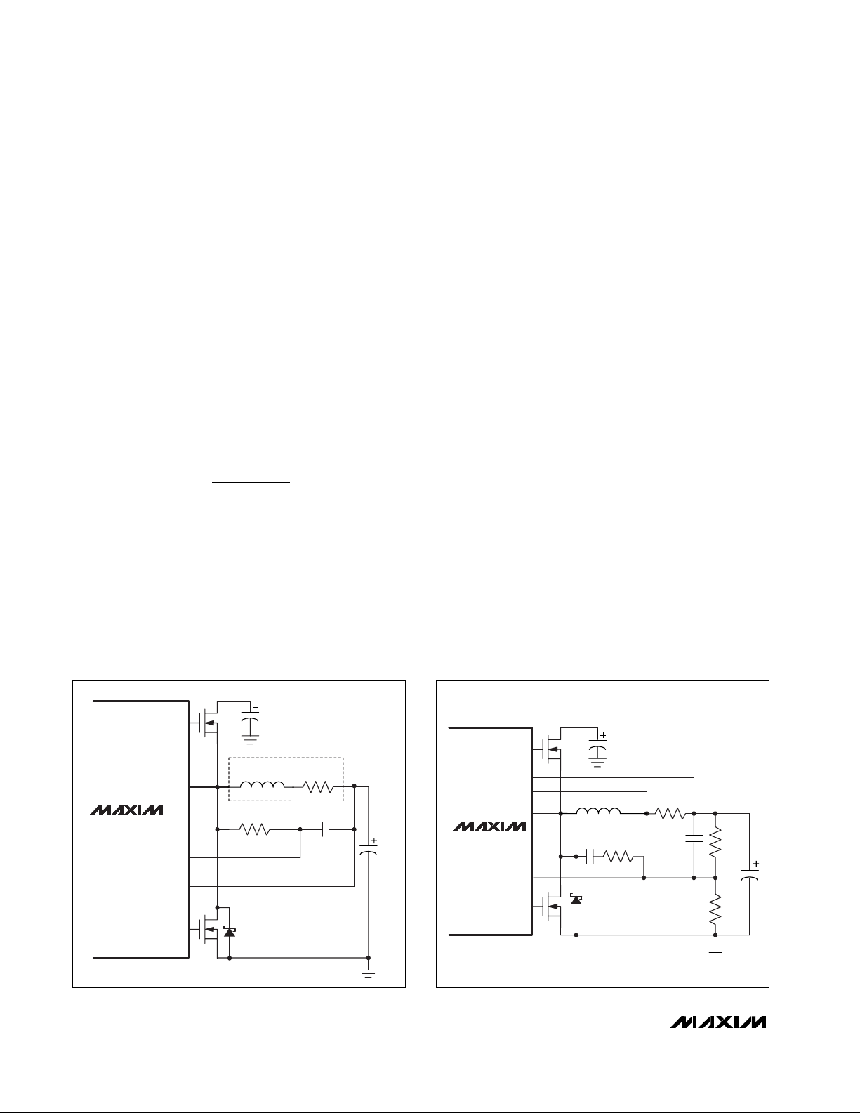
MAX8741/MAX8742
500kHz Multi-Output Power-Supply Controllers
with High Impedance in Shutdown
26 ______________________________________________________________________________________
scale down the voltage. Use the maximum inductance
and minimum DCR to get the maximum possible inductor time constant. Select RSand CSso that the maximum sense-network time constant is equal to or greater
than the maximum inductor time constant.
Reduced Output-Capacitance Application
In applications where higher output ripple is acceptable, lower output capacitance or higher ESR output
capacitors can be used. In such cases, cycle-by-cycle
stability is maintained by adding feed-forward compensation to offset for the increased output ESR. Figure 8
shows the addition of the feed-forward compensation
circuit. CFBprovides noise filtering, RFFis the feed-forward resistor, and CLXprovides DC blocking. Use
100pF for CFBand CLX. Select RFFaccording to the
equation below:
Set the value for R
FF
close to the calculation. Do not
make RFFtoo small as that introduces too much feedforward, possibly causing an overvoltage to be seen at
the feedback pin, and changing the mode of operation
to a voltage mode.
PC Board Layout Considerations
Good PC board layout is required in order to achieve
specified noise, efficiency, and stability performance.
The PC board layout artist must be given explicit
instructions, preferably a pencil sketch showing the
placement of power-switching components and highcurrent routing. A ground plane is essential for optimum
performance. In most applications, the circuit is located
on a multilayer board, and full use of the four or more
copper layers is recommended. Use the top layer for
high-current connections, the bottom layer for quiet
connections (REF, SS, GND), and the inner layers for
an uninterrupted ground plane. Use the following stepby-step guide:
1) Place the high-power components (Figure 1, C1, C3,
C4, Q1, Q2, L1, and R1) first, with their grounds
adjacent:
• Priority 1: Minimize current-sense resistor trace
lengths and ensure accurate current sensing with
Kelvin connections (Figure 9).
• Priority 2: Minimize ground trace lengths in the
high-current paths (discussed below).
• Priority 3: Minimize other trace lengths in the
high-current paths.
a) Use >5mm-wide traces
b) CIN to high-side MOSFET drain: 10mm max
length
c) Rectifier diode cathode to low-side MOSFET:
5mm max length
R
RLf
ESR
FF
≤
×××43
L
DL_
DH_
LX_
MAX8741
MAX8742
CSH_
CSL_
INDUCTOR
R
L
V
OUT
V
IN
C
IN
C
OUT
C
S
R
S
Figure 7. Lossless Inductor Current Sensing
R3
R4
FB_
L
C
IN
DL_
DH_
LX_
MAX8741
MAX8742
CSH_
CSL_
V
IN
C
LX
R
FF
C
FB
R
SENSE
V
OUT
C
OUT
Figure 8. Adding Feed-Forward Compensation
Page 27
MAX8741/MAX8742
500kHz Multi-Output Power-Supply Controllers
with High Impedance in Shutdown
______________________________________________________________________________________ 27
d) LX node (MOSFETs, rectifier cathode, induc
tor): 15mm max length
Ideally, surface-mount power components are butted up
to one another with their ground terminals almost touching. These high-current grounds are then connected to
each other with a wide filled zone of top-layer copper so
they do not go through vias. The resulting top layer “subground-plane” is connected to the normal inner-layer
ground plane at the output ground terminals, which
ensures that the IC’s analog ground is sensing at the supply’s output terminals without interference from IR drops
and ground noise. Other high-current paths should also
be minimized, but focusing primarily on short ground and
current-sense connections eliminates about 90% of all PC
board layout problems.
2) Place the IC and signal components. Keep the main
switching nodes (LX nodes) away from sensitive
analog components (current-sense traces and REF
capacitor). Place the IC and analog components on
the opposite side of the board from the powerswitching node. Important: The IC must be no more
than 10mm from the current-sense resistors. Keep
the gate-drive traces (DH_, DL_, and BST_) shorter
than 20mm and route them away from CSH_, CSL_,
and REF.
3) Use a single-point star ground where the input
ground trace, power ground (subground plane), and
normal ground plane meet at the supply’s output
ground terminal. Connect both IC ground pins and all
IC bypass capacitors to the normal ground plane.
MAX8741/MAX8742
SENSE RESISTOR
HIGH-CURRENT PATH
Figure 9. Kelvin Connections for the Current-Sense Resistors
Page 28

MAX8741/MAX8742
500kHz Multi-Output Power-Supply Controllers
with High Impedance in Shutdown
28 ______________________________________________________________________________________
2.2µF
5
RESET
FB5
MAX8742
PGND
SEQ
REF
11
9
15
12
13
14
20
19
17
16
Q3
Q4
T2
1:2.2
R2
D5
D2
18
POWER-GOOD
7
10 8
5V ON/OFF
SKIP
DL5
LX5
DH5
BST5
V
DD
2.2µF
0.1µF
C2
0.1µF
1µF
1N5819
5V OUTPUT
GND
2.5V REF
3
2
1
24
Q1
D1
Q2
L1
R1
0.1µF
0.1µF
1N5819
3.3V OUTPUT (3A)
ON/OFF
TIME/ON5
RUN/ON3
FB3
28
3V ON/OFF
26
25
27
CSL5
CSH5
CSL3
CSH3
DL3
LX3
DH3
BST3
SHDN
SYNC
INPUT
6.5V TO 28V
4
23
22
10Ω
621
V+ V
L
0.1µF
0.1µF
4.7µF
4.7µF
12OUT
C3
C1
C4
TO 3.3V OUTPUT TO 5V OUTPUT
12V AT 120mA
5V ALWAYS ON
Figure 10. Triple-Output Application for the MAX8742
Page 29

MAX8741/MAX8742
500kHz Multi-Output Power-Supply Controllers
with High Impedance in Shutdown
______________________________________________________________________________________ 29
OPEN
MAX8741
V+ SHDN V
L
SECFB
INPUT
6V TO 24V
C3
10Ω
ON/OFF
GND
REF SEQ SYNC
1µF
5V ALWAYS ON
Q1
ON/OFF
ON/OFF
0.1µF
0.1µF
4.7µF
4.7µF
0.1µF
Q3
DL3
CSH3
CSL3
FB3
RESET
RESET OUTPUT
SKIP
STEER
L1
R1
5V OUTPUT
C1
DL5
LX5
DH5
BST5
BST3
DH3
LX3
PGND
CSL5
CSH5
RUN/ON3
TIME/ON5
0Ω
FB5
0.1µF
0.1µF
L2 R2
3.3V OUTPUT
OPEN
0Ω
Q4
1N5819
Q2
1N5819
C2
Figure 11. Dual 6A Notebook Computer Power Supply
Page 30

MAX8741/MAX8742
500kHz Multi-Output Power-Supply Controllers
with High Impedance in Shutdown
30 ______________________________________________________________________________________
28
27
26
25
24
23
22
21
20
19
18
17
16
15
1
2
3
4
5
6
7
8
9
10
11
12
13
14
RUN/ON3
DH3
LX3
BST3
DL3
SHDN
SEQ
V+
V
L
PGND
DL5
BST5
LX5
DH5
CSH5
CSL5
FB5
RESET
SKIP
REF
GND
TIME/ON5
SYNC
V
DD
12OUT
FB3
CSL3
CSH3
SSOP
MAX8742
TOP VIEW
SSOP
28
27
26
25
24
23
22
21
20
19
18
17
16
15
1
2
3
4
5
6
7
8
9
10
11
12
13
14
RUN/ON3
DH3
LX3
BST3
DL3
SHDN
SEQ
V+
V
L
PGND
DL5
BST5
LX5
DH5
CSH5
CSL5
FB5
RESET
SKIP
REF
GND
TIME/ON5
SYNC
SECFB
STEER
FB3
CSL3
CSH3
MAX8741
32
31
30
29
28
27
26
N.C.
FB3
CSL3
CSH3
RUN/ON3
DH3
LX3
25 N.C.
9
10
11
12
13
14
15
RESET
FB5
CSL5
CSH5
SEQ
DH5
LX5
16N.C.
17
18
19
20
21
22
23
BST5
DL5
PGND
V
L
V+
SHDN
DL3
8
7
6
5
4
3
2
SKIP
REF
N.C.
GND
TIME/ON5
SYNC
SECFB
MAX8741
THIN QFN 5mm × 5mm
1STEER
24 BST3
32
31
30
29
28
27
26
N.C.
FB3
CSL3
CSH3
RUN/ON3
DH3
LX3
25 N.C.
9
10
11
12
13
14
15
RESET
FB5
CSL5
CSH5
SEQ
DH5
LX5
16N.C.
17
18
19
20
21
22
23
BST5
DL5
PGND
V
L
V+
SHDN
DL3
8
7
6
5
4
3
2
SKIP
REF
N.C.
GND
TIME/ON5
SYNC
V
DD
MAX8742
THIN QFN 5mm × 5mm
112OUT
24 BST3
Pin Configurations
Selector Guide
DEVICE AUXILIARY OUTPUT SECONDARY FEEDBACK
OVER/UNDERVOLTAGE
PROTECTION
MAX8741 None (SECFB input) Selectable (STEER pin) Yes
MAX8742 12V linear regulator Feeds into the 5V SMPS Yes
Page 31

MAX8741/MAX8742
500kHz Multi-Output Power-Supply Controllers
with High Impedance in Shutdown
______________________________________________________________________________________ 31
SSOP.EPS
PACKAGE OUTLINE, SSOP, 5.3 MM
1
1
21-0056
C
REV.DOCUMENT CONTROL NO.APPROVAL
PROPRIETARY INFORMATION
TITLE:
NOTES:
1. D&E DO NOT INCLUDE MOLD FLASH.
2. MOLD FLASH OR PROTRUSIONS NOT TO EXCEED .15 MM (.006").
3. CONTROLLING DIMENSION: MILLIMETERS.
4. MEETS JEDEC MO150.
5. LEADS TO BE COPLANAR WITHIN 0.10 MM.
7.90
H
L
0∞
0.301
0.025
8∞
0.311
0.037
0∞
7.65
0.63
8∞
0.95
MAX
5.38
MILLIMETERS
B
C
D
E
e
A1
DIM
A
SEE VARIATIONS
0.0256 BSC
0.010
0.004
0.205
0.002
0.015
0.008
0.212
0.008
INCHES
MIN
MAX
0.078
0.65 BSC
0.25
0.09
5.20
0.05
0.38
0.20
0.21
MIN
1.73 1.99
MILLIMETERS
6.07
6.07
10.07
8.07
7.07
INCHES
D
D
D
D
D
0.239
0.239
0.397
0.317
0.278
MIN
0.249
0.249
0.407
0.328
0.289
MAX
MIN
6.33
6.33
10.33
8.33
7.33
14L
16L
28L
24L
20L
MAX
N
A
D
e
A1
L
C
HE
N
12
B
0.068
Package Information
(The package drawing(s) in this data sheet may not reflect the most current specifications. For the latest package outline information,
go to www.maxim-ic.com/packages
.)
Page 32

Package Information (continued)
(The package drawing(s) in this data sheet may not reflect the most current specifications. For the latest package outline information,
go to www.maxim-ic.com/packages
.)
MAX8741/MAX8742
500kHz Multi-Output Power-Supply Controllers
with High Impedance in Shutdown
32 ______________________________________________________________________________________
QFN THIN.EPS
D2
(ND-1) X e
e
D
C
PIN # 1
I.D.
(NE-1) X e
E/2
E
0.08 C
0.10 C
A
A1 A3
DETAIL A
0.15
C B
0.15 C A
E2/2
E2
0.10 M C A B
PIN # 1 I.D.
b
0.35x45∞
L
D/2
D2/2
L
C
L
C
e e
L
CC
L
k
k
LL
E
1
2
21-0140
PACKAGE OUTLINE
16, 20, 28, 32, 40L, THIN QFN, 5x5x0.8mm
DETAIL B
L
L1
e
Page 33

MAX8741/MAX8742
500kHz Multi-Output Power-Supply Controllers
with High Impedance in Shutdown
Maxim cannot assume responsibility for use of any circuitry other than circuitry entirely embodied in a Maxim product. No circuit patent licenses are
implied. Maxim reserves the right to change the circuitry and specifications without notice at any time.
Maxim Integrated Products, 120 San Gabriel Drive, Sunnyvale, CA 94086 408-737-7600 ____________________ 33
© 2004 Maxim Integrated Products Printed USA is a registered trademark of Maxim Integrated Products.
Package Information (continued)
(The package drawing(s) in this data sheet may not reflect the most current specifications. For the latest package outline information,
go to www.maxim-ic.com/packages
.)
COMMON DIMENSIONS
3.353.15
T2855-1 3.25 3.353.15 3.25
MAX.
3.20
EXPOSED PAD VARIATIONS
3.00T2055-2 3.10
D2
NOM.MIN.
3.203.00 3.10
MIN.E2NOM. MAX.
NE
ND
PKG.
CODES
1. DIMENSIONING & TOLERANCING CONFORM TO ASME Y14.5M-1994.
2. ALL DIMENSIONS ARE IN MILLIMETERS. ANGLES ARE IN DEGREES.
3. N IS THE TOTAL NUMBER OF TERMINALS.
4. THE TERMINAL #1 IDENTIFIER AND TERMINAL NUMBERING CONVENTION SHALL CONFORM TO JESD 95-1
SPP-012. DETAILS OF TERMINAL #1 IDENTIFIER ARE OPTIONAL, BUT MUST BE LOCATED WITHIN THE
ZONE INDICATED. THE TERMINAL #1 IDENTIFIER MAY BE EITHER A MOLD OR MARKED FEATURE.
5. DIMENSION b APPLIES TO METALLIZED TERMINAL AND IS MEASURED BETWEEN 0.25 mm AND 0.30 mm
FROM TERMINAL TIP.
6. ND AND NE REFER TO THE NUMBER OF TERMINALS ON EACH D AND E SIDE RESPECTIVELY.
7. DEPOPULATION IS POSSIBLE IN A SYMMETRICAL FASHION.
8. COPLANARITY APPLIES TO THE EXPOSED HEAT SINK SLUG AS WELL AS THE TERMINALS.
9. DRAWING CONFORMS TO JEDEC MO220, EXCEPT EXPOSED PAD DIMENSION FOR T2855-1,
T2855-3 AND T2855-6.
NOTES:
SYMBOL
PKG.
N
L1
e
E
D
b
A3
A
A1
k
10. WARPAGE SHALL NOT EXCEED 0.10 mm.
JEDEC
T1655-1
3.203.00 3.10 3.00 3.10 3.20
0.70 0.800.75
4.90
4.90
0.25
0.250--
4
WHHB
4
16
0.350.30
5.10
5.105.00
0.80 BSC.
5.00
0.05
0.20 REF.
0.02
MIN. MAX.NOM.
16L 5x5
3.10
T3255-2
3.00
3.20
3.00 3.10 3.20
2.70
T2855-2 2.60 2.602.80 2.70 2.80
E
2
2
21-0140
PACKAGE OUTLINE
16, 20, 28, 32, 40L, THIN QFN, 5x5x0.8mm
L
0.30 0.500.40
---
---
WHHC
20
5
5
5.00
5.00
0.30
0.55
0.65 BSC.
0.45
0.25
4.90
4.90
0.25
0.65
--
5.10
5.10
0.35
20L 5x5
0.20 REF.
0.75
0.02
NOM.
0
0.70
MIN.
0.05
0.80
MAX.
---
WHHD-1
28
7
7
5.00
5.00
0.25
0.55
0.50 BSC.
0.45
0.25
4.90
4.90
0.20
0.65
--
5.10
5.10
0.30
28L 5x5
0.20 REF.
0.75
0.02
NOM.
0
0.70
MIN.
0.05
0.80
MAX.
---
WHHD-2
32
8
8
5.00
5.00
0.40
0.50 BSC.
0.30
0.25
4.90
4.90
0.50
--
5.10
5.10
32L 5x5
0.20 REF.
0.75
0.02
NOM.
0
0.70
MIN.
0.05
0.80
MAX.
-
40
10
10
5.00
5.00
0.20
0.50
0.40 BSC.
0.40
0.25
4.90
4.90
0.15
0.60
5.10
5.10
0.25
40L 5x5
0.20 REF.
0.75
NOM.
0
0.70
MIN.
0.05
0.80
MAX.
0.20 0.25 0.30
-
0.35 0.45
0.30 0.40 0.50
DOWN
BONDS
ALLOWED
NO
YES3.103.00 3.203.103.00 3.20T2055-3
3.103.00 3.203.103.00 3.20T2055-4
T2855-3 3.15 3.25 3.35 3.15 3.25 3.35
T2855-6 3.15 3.25 3.35 3.15 3.25 3.35
T2855-4 2.60 2.70 2.80 2.60 2.70 2.80
T2855-5 2.60 2.70 2.80 2.60 2.70 2.80
T2855-7 2.60 2.70
2.80
2.60 2.70 2.80
3.20
3.00 3.10T3255-3 3.203.00 3.10
3.203.00 3.10T3255-4 3.203.00 3.10
3.403.20 3.30T4055-1 3.20 3.30 3.40
NO
NO
NO
NO
NO
NO
NO
NO
YES
YES
YES
YES
YES
3.203.00T1655-2 3.10 3.00 3.10 3.20 YES
 Loading...