

Page 1
MAX8730
Low-Cost Battery Charger
________________________________________________________________ Maxim Integrated Products 1
19-3885; Rev 0; 12/05
For pricing, delivery, and ordering information, please contact Maxim/Dallas Direct! at
1-888-629-4642, or visit Maxim’s website at www.maxim-ic.com.
EVALUATION KIT
AVAILABLE
General Description
The MAX8730 highly integrated, multichemistry, batterycharger control IC simplifies construction of accurate
and efficient chargers. The MAX8730 operates at high
switching frequency to minimize external component
size and cost. The MAX8730 uses analog inputs to control charge current and voltage, and can be programmed by a microcontroller or hardwired.
The MAX8730 reduces charge current to give priority to
the system load, effectively limiting the adapter current
and reducing the adapter current requirements.
The MAX8730 provides a digital output that indicates
the presence of an AC adapter, and an analog output
that monitors the current drawn from the AC adapter.
Based on the presence and absence of the AC
adapter, the MAX8730 automatically selects the appropriate source for supplying power to the system by controlling two external switches. Under system control, the
MAX8730 allows the battery to undergo a relearning
cycle in which the battery is completely discharged
through the system load and then recharged.
An analog output indicates adapter current or batterydischarge current. The MAX8730 provides a low-quiescent-current linear regulator, which may be used when
the adapter is absent, or disabled for reduced current
consumption
The MAX8730 is available in a small, 5mm x 5mm, 28pin, thin (0.8mm) QFN package. An evaluation kit is
available to reduce design time. The MAX8730 is
available in a lead-free package.
Applications
Notebook Computers
Tablet PCs
Portable Equipment with Rechargeable Batteries
Features
♦ Small Inductor (3.5µH)
♦ Programmable Charge Current > 4.5A
♦ Automatic Power-Source Selection
♦ Analog Inputs Control Charge Current and
Charge Voltage
♦ Monitor Outputs for
AC Adapter Current
Battery-Discharge Current
AC Adapter Presence
♦ Independent 3.3V 20mA Linear Regulator
♦ Up to 17.6V (max) Battery Voltage
♦ +8V to +28V Input Voltage Range
♦ Reverse Adapter Protection
♦ System Short-Circuit Protection
♦ Cycle-by-Cycle Current Limit
Ordering Information
PART
TEMP
RANGE
PINPACKAGE
PKG
CODE
MAX8730ETI+
28 Thin QFN
(5mm x 5mm)
T2855-5
+Denotes lead-free package.
Pin Configuration appears at end of data sheet.
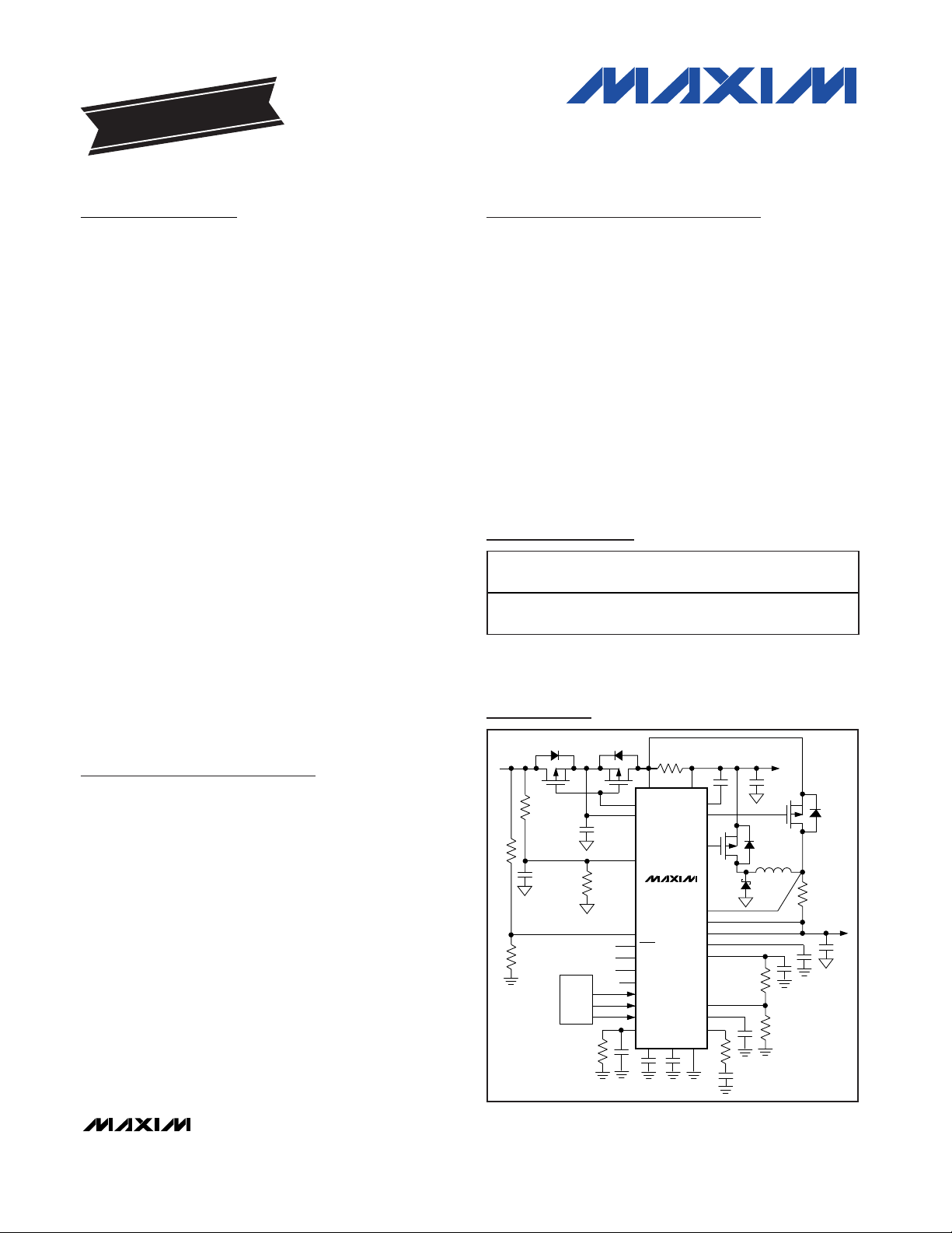
MAX8730
ADAPTER
INPUT
PDS
SRC
ASNS
ACIN
ACOK
VCTL
LDO
CLS
ICTL
MODE
REFON
INPON
LDO
RELTH
REF
SWREF
BATT
CSIN
CSIP
DHI
PDL
DHIV
IINP CCV
CCI
CCS
CSSP CSSN
GND
REF
HOST
SYSTEM
LOAD
BATTERY
Typical Operating Circuit
-40°C to +85°C
Page 2
MAX8730
Low-Cost Battery Charger
2 _______________________________________________________________________________________
ABSOLUTE MAXIMUM RATINGS
ELECTRICAL CHARACTERISTICS
(Circuit of Figure 1. V
SRC
= V
ASNS
= V
CSSP
= V
CSSN
= 18V, V
BATT
= V
CSIP
= V
CSIN
= 12V, V
VCTL
= V
ICTL
= 1.8V, MODE = float,
ACIN = 0, CLS = REF, REFON = LDO, INPON = LDO, RELTH = 2V. T
A
= 0°C to +85°C, unless otherwise noted. Typical values are at
T
A
= +25°C.)
Stresses beyond those listed under “Absolute Maximum Ratings” may cause permanent damage to the device. These are stress ratings only, and functional
operation of the device at these or any other conditions beyond those indicated in the operational sections of the specifications is not implied. Exposure to
absolute maximum rating conditions for extended periods may affect device reliability.
CSSP, SRC, ACOK, ASNS, DHIV, BATT,
CSIP to GND.......................................................-0.3V to +30V
CSIP to CSIN or CSSP to CSSN ............................-0.3V to +0.3V
DHIV to SRC .................................................-6V to (SRC + 0.3V)
DHI to DHIV ...............................................-0.3V to (SRC + 0.3V)
PDL, PDS to GND ........................................-0.3V to (SRC + 0.3)
CCI, CCS, CCV, IINP, SWREF, REF,
MODE, ACIN to GND.............................-0.3V to (LDO + 0.3V)
RELTH, VCTL, ICTL, REFON, CLS, LDO,
INPON to GND .....................................................-0.3V to +6V
LDO Short-Circuit Current...................................................50mA
Continuous Power Dissipation (T
A
= +70°C)
28-Pin TQFN (derate 20.8mW/°C above +70°C) .......1667mW
Operating Temperature Range ...........................-40°C to +85°C
Junction Temperature ............................................................+150°C
Storage Temperature Range .............................-60°C to +150°C
Lead Temperature (soldering, 10s) .................................+300°C
PARAMETER
SYMBOL
CONDITIONS
MIN
TYP
MAX
UNITS
CHARGE-VOLTAGE REGULATION
VCTL Range 0 3.6 V
Not including resistor
tolerances
V
VCTL
= 3.6V
or 0V
Including 1% resistor
tolerances
Battery-Regulation Voltage
Accuracy
V
VCTL
= V
LDO
(3 or 4 cells)
%
V
VCTL
Default Threshold V
VCTL
rising 4.4 V
V
VCTL
= 3V
0 4
VCTL Input Bias Current
SRC = BATT, ASNS = GND INPON =
REFON = 0, V
VCTL
= 5V
0 16
µA
CHARGE-CURRENT REGULATION
ICTL Range 0 3.6 V
mV
V
ICTL
= 3.6V
-5 +5 %
75
mV
Full-Charge-Current Accuracy
(CSIP to CSIN)
V
I
CTL
= 2.0V
-5 +5 %
Trickle-Charge-Current Accuracy
V
ICTL
= 120mV 2.5 4.5 7.5 mV
Charge-Current Gain Error Based on V
ICTL
= 3.6V and V
ICTL
= 0.12V
%
Charge-Current Offset Error Based on V
ICTL
= 3.6V and V
ICTL
= 0.12V -2 +2 mV
BATT/CSIP/CSIN Input Voltage
Range
0 19 V
Charging enabled
600
CSIP/CSIN Input Current
Charging disabled, SRC = BATT,
ASNS = GND or V
ICTL
= 0V
8 16
µA
-1.0
-1.05
-0.5
128.25 135 141.75
71.25
-1.9
300
+1.0
+1.05
+0.5
78.75
+1.9
Page 3

MAX8730
Low-Cost Battery Charger
_______________________________________________________________________________________ 3
ELECTRICAL CHARACTERISTICS (continued)
(Circuit of Figure 1. V
SRC
= V
ASNS
= V
CSSP
= V
CSSN
= 18V, V
BATT
= V
CSIP
= V
CSIN
= 12V, V
VCTL
= V
ICTL
= 1.8V, MODE = float,
ACIN = 0, CLS = REF, REFON = LDO, INPON = LDO, RELTH = 2V. T
A
= 0°C to +85°C, unless otherwise noted. Typical values are at
T
A
= +25°C.)
PARAMETER
CONDITIONS
UNITS
ICTL falling 50 65 80
ICTL Power-Down Mode
Threshold
ICTL rising 70 90 110
mV
V
ICTL
= 3V -1 +1
ICTL Input Bias Current
SRC = BATT, ASNS = GND, V
ICTL
= 5V
-1 +1
µA
CSSP-to-CSSN Full-Scale
Current-Sense Voltage
mV
mV
V
CLS
= REF (trim point)
-4 +4 %
50 53 56 mV
V
CLS
= REF x 0.7
%
36 38
mV
Input Current-Limit Accuracy
V
CLS
= REF x 0.5
%
CSSP/CSSN Input Voltage Range
8.0 28 V
V
CSSP
= V
CSSN
= V
SRC
> 8.0V
800
CSSP/CSSN Input Current
V
SRC
= 0V 0.1 1
µA
CLS Input Range 1.1
V
CLS Input Bias Current V
CLS
= 2.0V -1 +1 µA
IINP Transconductance V
CSSP
- V
CSSN
= 56mV
2.8
µA/mV
V
CSSP
- V
CSSN
= 100mV, V
IINP
= 0 to 4.5V -5 +5
V
CSSP
- V
CSSN
= 75mV -8 +8
V
CSSP
- V
CSSN
= 56mV -5 +5
IINP Accuracy
V
CSSP
- V
CSSN
= 20mV
%
IINP Gain Error Based on V
IC T L =
RE F x 0.5 and V
IC T L
= RE F -7 +7 %
IINP Offset Error Based on V
IC T L =
RE F x 0.5 and V
IC T L
= RE F -2 +2 mV
IINP Fault threshold IINP rising 4.1 4.2 4.3 V
SUPPLY AND LINEAR REGULATOR
SRC Input Voltage Range 8.0 28 V
SRC falling 7 7.4
SRC Undervoltage Lockout
Threshold
SRC rising 7.5 8
V
SYMBOL
MIN TYP MAX
72.75 75.75 78.75
72.75 75.75 78.75
-5.6
-6.6
2.66
-12.5
+5.6
40.5
+6.6
400
REF
2.94
+12.5
Page 4
MAX8730
Low-Cost Battery Charger
4 _______________________________________________________________________________________
ELECTRICAL CHARACTERISTICS (continued)
(Circuit of Figure 1. V
SRC
= V
ASNS
= V
CSSP
= V
CSSN
= 18V, V
BATT
= V
CSIP
= V
CSIN
= 12V, V
VCTL
= V
ICTL
= 1.8V, MODE = float,
ACIN = 0, CLS = REF, REFON = LDO, INPON = LDO, RELTH = 2V. T
A
= 0°C to +85°C, unless otherwise noted. Typical values are at
T
A
= +25°C.)
PARAMETER
SYMBOL
CONDITIONS
MIN
TYP
MAX
UNITS
Normal mode 4 6 mA
10 20
V
INPON = low,
V
REFON
= high
600
V
INPON = high,
V
REFON
= low
600
SRC Quiescent Current
(INPON/REFON = Don’t Care)
V
SRC
= V
BATT =
12V, ASNS =
GND
(Note 2)
600
µA
V
BATT
= 16.8V, V
SRC
= 19V, ICTL = 0 8 16
BATT Input Current
V
BATT
= 2V to 19V, V
SRC
> V
BATT
+ 0.3V
600
µA
I
CSIP
+ I
CSIN
+ I
BATT
, ASNS = GND 2 5
600
Battery-Leakage Current
I
CSIP
+ I
CSIN
+ I
BATT
+
I
CSSP
+ I
CSSN
+ I
SRC
,
ASNS = REFON = GND
2 5
µA
LDO Output Voltage 8.0V < V
SRC
< 28V, no load 5.2
5.5 V
LDO Load Regulation 0 < I
LDO
< 10mA 20 50 mV
LDO Undervoltage Lockout
Threshold
V
SRC
= 8.0V 4 V
REFERENCES
REF Output Voltage Ref
V
REF Undervoltage Lockout
Threshold
REF falling 3.1 3.9 V
SWREF Output Voltage 8.0V < V
SRC
< 28V, no load
3.3
V
SWREF Load Regulation 0.1mA < I
SWREF
< 20mA
20 50 mV
TRIP POINTS
ACIN Threshold ACIN rising
2.1
V
ACIN Threshold Hysteresis 60 mV
ACIN Input Bias Current V
ACIN
= 2.048V -1 +1 µA
SWITCHING REGULATOR
DHI Off-Time V
BATT
= 16.0V
400 ns
DHI Off-Time K Factor V
BATT
= 16.0V 4.8 5.6 6.4
V x µs
Sense Voltage for Minimum
Discontinuous Mode Ripple
Current
V
CSIP
- V
CSIN
7 mV
Cycle-by-Cycle Current-Limit
Sense Voltage
240 mV
Charge Disable Threshold V
SRC
- V
BATT
, SRC falling 40 60 80 mV
DHIV Output Voltage With respect to SRC
-5.5 V
DHIV Sink Current 10 mA
V
INPON =VREFON
= low
300
300
V
INPON = VREFON
V
INPON = GND
= high
= 5.4V
REFON
4.18 4.20 4.22
3.234
2.037
300 350
160 200
-4.3 -4.8
350
300
300
5.35
3.366
2.163
Page 5
MAX8730
Low-Cost Battery Charger
_______________________________________________________________________________________ 5
ELECTRICAL CHARACTERISTICS (continued)
(Circuit of Figure 1. V
SRC
= V
ASNS
= V
CSSP
= V
CSSN
= 18V, V
BATT
= V
CSIP
= V
CSIN
= 12V, V
VCTL
= V
ICTL
= 1.8V, MODE = float,
ACIN = 0, CLS = REF, REFON = LDO, INPON = LDO, RELTH = 2V. T
A
= 0°C to +85°C, unless otherwise noted. Typical values are at
T
A
= +25°C.)
PARAMETER
SYMBOL
CONDITIONS
MIN
TYP
MAX
UNITS
DHI Resistance Low I
DHI
= -10mA 2 4 Ω
DHI Resistance High I
DHI
= 10mA 1 2 Ω
ERROR AMPLIFIERS
V C TL = 3.6V , V
BAT T
= 16.8V , M OD E = LD O
GMV Loop Transconductance
mA/V
GMI Loop Transconductance ICTL = 3.6V, V
CSSP
- V
CSIN
= 75mV 0.5 1 2
mA/V
GMS Loop Transconductance V
CLS
= 2.048V, V
CSSP
- V
CSSN
= 75mV 0.5 1 2
mA/V
CCI/CCS/CCV Clamp Voltage
1.1V < V
CCV
< 3.0V,
1.1V < V
CCI
< 3.0V,
1.1V < V
CCS
< 3.0V
600 mV
LOGIC LEVELS
MODE, REFON Input Low Voltage
0.5 V
MODE Input Middle Voltage 1.9
3.3 V
M OD E , RE FON Inp ut H i g h V ol tag e
3.4 V
MODE, REFON, INPON Input
Bias Current
MODE = 0 or 3.6V -2 +2 µA
V
INPON
rising
V
INPON Threshold
V
INPON
falling 0.8 V
ADAPTER DETECTION
ACOK Voltage Range 0 28 V
ACOK Sink Current V
ACOK
= 0.4V, ACIN = 1.5V 1 mA
ACOK Leakage Current V
ACOK
= 28V, ACIN = 2.5V 1 µA
BATTERY DETECTION
BATT Overvoltage Threshold
V
VCTL
= V
LDO
, BATT
rising; result with respect
to battery-set voltage
mV
BATT Overvoltage Hysteresis
mV
RELTH Operating Voltage Range
0.9 2.6 V
RELTH Input Bias Current V
RELTH
= 0.9V to 2.6V
-50 +50 nA
V
RELTH
= 0.9V
4.5
BATT Minimum Voltage Trip
Threshold
V
BATT
falling
V
RELTH
= 2.6V
V
PDS, PDL SWITCH CONTROL
Adapter-Absence Detect
Threshold
V
ASNS
- V
BATT
, V
ASNS
falling
mV
Adapter-Detect Threshold V
ASNS
- V
BATT
-60 mV
PDS Output Low Voltage Result with respect to SRC, I
PDS
= 0 -8 -10 -12 V
PDS/PDL Output High Voltage Result with respect to SRC, I
PD_
= 0
-0.5 V
PDS/PDL Turn-Off Current V
PDS
= V
SRC
- 2V, V
SRC
= 16V 6 12 mA
0.0625 0.125 0.250
V C TL = 3.6V , V
= 12.6V , M OD E = FLOAT 0.0833 0.167 0.333
BAT T
150 300
2.65
2.2
V
MODE
V
MODE
= V
= FLOAT
LDO
+140
+100
100
4.42
12.77 13.0 13.23
-300 -280 -240
-140 -100
-0.2
4.58
Page 6
MAX8730
Low-Cost Battery Charger
6 _______________________________________________________________________________________
ELECTRICAL CHARACTERISTICS (continued)
(Circuit of Figure 1. V
SRC
= V
ASNS
= V
CSSP
= V
CSSN
= 18V, V
BATT
= V
CSIP
= V
CSIN
= 12V, V
VCTL
= V
ICTL
= 1.8V, MODE = float,
ACIN = 0, CLS = REF, REFON = LDO, INPON = LDO, RELTH = 2V. T
A
= 0°C to +85°C, unless otherwise noted. Typical values are at
T
A
= +25°C.)
ELECTRICAL CHARACTERISTICS
(Circuit of Figure 1. V
SRC
= V
ASNS
= V
CSSP
= V
CSSN
= 18V, V
BATT
= V
CSIP
= V
CSIN
= 12V, V
VCTL
= V
ICTL
= 1.8V, MODE = float,
ACIN = 0, CLS = REF, REFON = LDO, INPON = LDO, RELTH = 2V. T
A
= -40°C to +85°C, unless otherwise noted.)
PARAMETER
CONDITIONS
UNITS
PDS Turn-On Current PDS = SRC 6 12 mA
PDL Turn-On Resistance PDL = GND 50
200 kΩ
PDS/PDL Delay Time 5.0 µs
SYMBOL
CHARGE-VOLTAGE REGULATION
PARAMETER SYMBOL CONDITIONS MIN TYP MAX UNITS
VCTL Range 0 3.6 V
Battery-Regulation-Voltage
Accuracy
V
Default Threshold V
VCTL
VCTL Input Bias Current
CHARGE-CURRENT REGULATION
ICTL Range 0 3.6 V
Full-Charge-Current Accuracy
(CSIP to CSIN)
Trickle-Charge-Current Accuracy V
Charge-Current Gain Error Based on V
Charge-Current Offset Error Based on V
BATT/CSIP/CSIN Input Voltage
Range
CSIP/CSIN Input Current
ICTL Power-Down Mode
Threshold
V
= 3.6V
VCTL
or 0V
V
= V
VCTL
rising 4.4 V
VCTL
SRC = BATT, ASNS = GND INPON =
REFON = 0, V
V
= 3.6V
ICTL
V
= 2.0V
ICTL
= 120mV 2 10 mV
ICTL
0 19 V
Charging enabled 1000
Charging disabled, SRC = BATT,
ASNS = GND, or V
ICTL falling 50 80
ICTL rising 70 110
MIN TYP MAX
100
Not including resistor
tolerances
Including 1% resistor
tolerances
(3 or 4 cells) -0.8 +0.8
LDO
VCTL
-1.2 +1.2
-1.25
= 5V
0 16 µA
128.25 141.75 mV
-5 +5 %
70 80 mV
-6.7 +6.7 %
= 3.6V and V
ICTL
= 3.6V and V
ICTL
ICTL
= 0V
= 0.12V -1.9 +1.9 %
ICTL
= 0.12V -2 +2 mV
ICTL
16
+1.25
%
µA
mV
Page 7
MAX8730
Low-Cost Battery Charger
_______________________________________________________________________________________ 7
PARAMETER
SYMBOL
CONDITIONS
MIN
TYP
MAX
UNITS
INPUT-CURRENT REGULATION
CSSP-to-CSSN Full-Scale
Current-Sense Voltage
mV
V
CLS
= REF (trim point)
mV
V
CLS
= REF x 0.7
mVInput Current-Limit Accuracy
V
CLS
= REF x 0.5
mV
CSSP/CSSN Input Voltage Range
8.0 28 V
CSSP/CSSN Input Current V
CSSP
= V
CSSN
= V
SRC
> 8.0V
µA
CLS Input Range 1.1
V
IINP Transconductance V
CSSP
- V
CSSN
= 56mV
µA/mV
V
CSSP
- V
CSSN
= 100mV, V
IINP
= 0 to 4.5V
-5 +5
V
CSSP
- V
CSSN
= 75mV -8 +8
V
CSSP
- V
CSSN
= 56mV -5 +5
IINP Accuracy
V
CSSP
- V
CSSN
= 20mV
%
IINP Gain Error
-7 +7 %
IINP Offset Error
-2 +2 mV
IINP Fault Threshold IINP rising 4.1 4.3 V
SUPPLY AND LINEAR REGULATOR
SRC Input Voltage Range 8.0 28 V
SRC falling 7
SRC Undervoltage Lockout
Threshold
SRC rising 8
V
Normal mode 6 mA
20
V
INPON = low,
V
REFON
= high
600
V
INPON = high,
V
REFON
= low
600
SRC Quiescent Current
(INPON/REFON = Don’t Care)
SRC
= V
BATT =
12V, ASNS =
GND
(Note 2)
600
µA
BATT Input Current
600 µA
600
Battery Leakage Current
I
CSIP
+ I
CSIN
+ I
BATT
+ I
CSSP
+ I
CSSN
+ I
SRC
,
ASNS = REFON = GND
16
µA
LDO Output Voltage 8.0V < VSRC < 28V, no load 5.2 5.5 V
LDO Load Regulation 0 < I
LDO
< 10mA 50 mV
ELECTRICAL CHARACTERISTICS (continued)
(Circuit of Figure 1. V
SRC
= V
ASNS
= V
CSSP
= V
CSSN
= 18V, V
BATT
= V
CSIP
= V
CSIN
= 12V, V
VCTL
= V
ICTL
= 1.8V, MODE = float,
ACIN = 0, CLS = REF, REFON = LDO, INPON = LDO, RELTH = 2V. T
A
= -40°C to +85°C, unless otherwise noted.)
Based on V
Based on V
RE F x 0.5 and V
I C T L =
RE F x 0.5 and V
I C T L =
= RE F
I C T L
= RE F
I C T L
72.75
72.75
36.00
50.0
2.66
-12.5
78.25
78.25
56.0
40.50
1000
REF
2.94
+12.5
V
INPON = VREFON
= low
V
INPON = VREFON
V
= 2V to 19V, V
BATT
SRC
> V
V
INPON = GND
BATT
REFON
= high
+ 0.3V
= 5.4V
Page 8
MAX8730
Low-Cost Battery Charger
8 _______________________________________________________________________________________
PARAMETER
CONDITIONS
UNITS
REFERENCES
REF Output Voltage Ref 0 < I
REF
< 500µA
V
REF Undervoltage Lockout
Threshold
REF falling 3.9 V
SWREF Output Voltage 8.0V < V
SRC
< 28V, no load
V
SWREF Load Regulation 0.1mA < I
SWREF
< 20mA 50 mV
TRIP POINTS
ACIN Threshold ACIN rising
V
SWITCHING REGULATOR
DHI Off-Time V
BATT
= 16.0V 300 400 ns
DHI Off-Time K Factor V
BATT
= 16.0V 4.8 6.4
V x µs
Cycle-by-Cycle Current-Limit
Sense Voltage
160 240 mV
DHIV Output Volatge With respect to SRC
V
DHIV Sink Current 10 mA
DHI Resistance Low I
DHI
= -10mA 4 Ω
DHI Resistance High I
DHI
= 10mA 2 Ω
ERROR AMPLIFIERS
V C TL = 3.6V , V
BAT T
= 16.8V , M OD E = LD O
GMV Loop Transconductance
mA/V
GMI Loop Transconductance ICTL = 3.6V, V
CSSP
- V
CSIN
= 75mV 0.5 2
mA/V
GMS Loop Transconductance V
CLS
= 2.048V, V
CSSP
- V
CSSN
= 75mV 0.5 2
mA/V
CCI/CCS/CCV Clamp Voltage
1.1V < V
CCV
< 3.0V, 1.1V < V
CCI
< 3.0V,
1.1V < V
CCS
< 3.0V
150 600 mV
LOGIC LEVELS
M OD E , RE FON Inp ut Low V ol tag e 0.5 V
MODE Input Middle Voltage 1.9 3.3 V
M OD E , RE FON Inp ut H i g h V ol tag e
3.4 V
V
INPON
rising
INPON Threshold
V
INPON
falling 0.8
V
ADAPTER DETECTION
ACOK Voltage Range 0 28 V
ACOK Sink Current V
ACOK
= 0.4V, ACIN = 1.5V 1 mA
ELECTRICAL CHARACTERISTICS (continued)
(Circuit of Figure 1. V
SRC
= V
ASNS
= V
CSSP
= V
CSSN
= 18V, V
BATT
= V
CSIP
= V
CSIN
= 12V, V
VCTL
= V
ICTL
= 1.8V, MODE = float,
ACIN = 0, CLS = REF, REFON = LDO, INPON = LDO, RELTH = 2V. T
A
= -40°C to +85°C, unless otherwise noted.)
SYMBOL
MIN TYP MAX
4.16
3.224
2.037
V C TL = 3.6V , V
-4.3
0.0625
= 12.6V , M OD E = FLOAT 0.0833
BAT T
2.2
4.24
3.376
2.163
-5.5
0.250
0.333
Page 9
MAX8730
Low-Cost Battery Charger
_______________________________________________________________________________________ 9
Note 1: Accuracy does not include errors due to external-resistance tolerances.
Note 2: In this mode, SRC current is drawn from the battery.
PARAMETER
SYMBOL
CONDITIONS
MIN
TYP
MAX
UNITS
BATTERY DETECTION
RELTH Operating Voltage Range
0.9 2.6 V
BATT Minimum Voltage Trip
Threshold
V
BATT
falling
V
PDS, PDL SWITCH CONTROL
Adapter-Absence-Detect
Threshold
V
ASNS
- V
BATT
, V
ASNS
falling
mV
Adapter-Detect Threshold V
ASNS
- V
BATT
-60 mV
PDS Output Low Voltage Result with respect to SRC, I
PDS
= 0 -7 -12 V
PDS/PDL Output High Voltage Result with respect to SRC, I
PD_
= 0
V
PDS/ PDL Turn-Off Current V
PDS
= V
SRC
- 2V, V
SRC
= 16V 6 mA
PDS Turn-On Current PDS = SRC 6 mA
PDL Turn-On Resistance PDL = GND 50
200 kΩ
ELECTRICAL CHARACTERISTICS (continued)
(Circuit of Figure 1. V
SRC
= V
ASNS
= V
CSSP
= V
CSSN
= 18V, V
BATT
= V
CSIP
= V
CSIN
= 12V, V
VCTL
= V
ICTL
= 1.8V, MODE = float,
ACIN = 0, CLS = REF, REFON = LDO, INPON = LDO, RELTH = 2V. T
A
= -40°C to +85°C, unless otherwise noted.)
V
RELTH
V
RELTH
= 0.9V
= 2.6V
4.42
12.77
-310
-140
4.58
13.23
-240
-0.5
100
Page 10

MAX8730
Low-Cost Battery Charger
10 ______________________________________________________________________________________
Typical Operating Characteristics
(Circuit of Figure 1, adapter = 19.5V, V
BATT
= 12V, V
ICTL
= 2.4V, MODE > 1.8V, REFON = INPON = LDO, V
RELTH
= V
REF
/2, TA =
+25°C, unless otherwise noted.)
TRICKLE-CHARGE CURRENT
vs. BATTERY VOLTAGE
BATTERY VOLTAGE (V)
TRICKLE-CHARGE-CURRENT ERROR (%)
MAX8730 toc07
0369121518
-25
-20
-15
-10
-5
0
5
10
15
20
25
CHARGE CURRENT = 150mA
BATTERY-VOLTAGE ERROR
vs. CHARGE CURRENT
CHARGE CURRENT (A)
BATTERY-VOLTAGE ERROR (%)
MAX8730 toc08
0 0.5 1.0 1.5 2.0 2.5 3.0 3.5
-0.25
-0.20
-0.15
-0.10
-0.05
0
4 CELLS
3 CELLS
BATTERY-VOLTAGE ERROR vs. VCTL
VCTL (V)
CHARGE-VOLTAGE ERROR (%)
MAX8730 toc09
0 1.50.5 1.0 2.0 2.5 3.0 3.5
-1.0
-0.8
-0.6
-0.4
-0.2
0
0.2
0.4
0.6
0.8
1.0
INPUT CURRENT-LIMIT ERROR vs. CLS
V
CLS
(V)
INPUT CURRENT-LIMIT ERROR (%)
MAX8730 toc01
1.1 1.6 2.1 2.6 3.1 3.6 4.1
-15
-10
-5
0
5
10
15
TYPICAL UNIT
MINIMUM
MAXIMUM
INPUT CURRENT-LIMIT ERROR
vs. SYSTEM CURRENT
SYSTEM CURRENT (A)
INPUT CURRENT-LIMIT ERROR (%)
0 0.5 1.0 1.5 2.0 2.5 3.0 3.5
0
0.5
1.0
1.5
2.0
2.5
3.0
3.5
4.0
4.5
5.0
VIN = 17V
VIN = 19V
VIN = 24V
V
CLS
= V
REF
x 0.7
INPUT CURRENT-LIMIT ERROR
vs. SYSTEM CURRENT
SYSTEM CURRENT (A)
INPUT CURRENT-LIMIT ERROR (%)
MAX8730 toc03
012345
0
1
2
3
4
5
6
7
V
CLS
= V
REF
/ 2
V
CLS
= V
REF
x 0.7
V
CLS
= V
REF
IINP ERROR vs. V
CSSP
- V
CSSN
MAX8730 toc04
V
CSSP
- V
CSSN
IINP ERROR (%)
908070605040302010
-10
-5
0
5
10
15
-15
0 100
MINIMUM
MAXIMUM
CHARGE-CURRENT ERROR
vs. CHARGE-CURRENT SETTING
V
ICTL
(V)
CHARGE-CURRENT ERROR (%)
MAX8730 toc05
0 0.6 1.2 1.8 2.4 3.0 3.6
-20
-15
-10
-5
0
5
10
15
20
TYPICAL UNIT
MINIMUM ERROR
MAXIMUM ERROR
CHARGE-CURRENT ERROR
vs. BATTERY VOLTAGE
BATTERY VOLTAGE (V)
CHARGE-CURRENT ERROR (%)
MAX8730 toc06
051015 20
-0.5
-0.2
0.1
0.4
0.7
1.0
1.3
1.6
V
ICTL
= 2V
V
ICTL
= 3.6V
Page 11

MAX8730
Low-Cost Battery Charger
______________________________________________________________________________________ 11
OUTPUT RIPPLE VOLTAGE
vs. BATTERY VOLTAGE
BATTERY VOLTAGE (V)
OUTPUT RIPPLE VOLTAGE (mV
P-P
)
MAX8730 toc10
051015 20
0
0.03
0.06
0.09
0.12
0.15
0.18
Typical Operating Characteristics (continued)
(Circuit of Figure 1, adapter = 19.5V, V
BATT
= 12V, V
ICTL
= 2.4V, MODE > 1.8V, REFON = INPON = LDO, V
RELTH
= V
REF
/2, TA =
+25°C, unless otherwise noted.)
SWITCHING FREQUENCY
vs. BATTERY VOLTAGE
BATTERY VOLTAGE (V)
SWITCHING FREQUENCY (kHz)
MAX8730 toc11
0369121518
200
400
600
800
1000
ADAPTER INSERTION
MAX8730toc13
0V
20V
20V
0V
20V
0V
20V
0V
100µs/div
ADAPTER
PDS
PDL
SYSTEM
LOAD
ADAPTER
INSERTION
SYSTEM LOAD TRANSIENT
MAX8730toc15
0A
5A
5A
0A
5A
0A
500mV/div
200µs/div
LOAD
CURRENT
ADAPTER
CURRENT
INDUCTOR
CURRENT
COMPENSATION
CCS
CCI
CCS
CCI
BATTERY REMOVAL
CHARGE
CURRENT = 12V
C
OUT
MAX8730toc12
= 4.7µF
13V
12.5V
ADAPTER
C
= 10µF
OUT
4µs/div
ADAPTER REMOVAL
PDS
4ms/div
PDL
SYSTEM
LOAD
MAX8730toc14
BATTERY
VOLTAGE = 16.8V
20V
0V
20V
0V
20V
0V
20V
0V
Page 12

MAX8730
Low-Cost Battery Charger
12 ______________________________________________________________________________________
Typical Operating Characteristics (continued)
(Circuit of Figure 1, adapter = 19.5V, V
BATT
= 12V, V
ICTL
= 2.4V, MODE > 1.8V, REFON = INPON = LDO, V
RELTH
= V
REF
/2, TA =
+25°C, unless otherwise noted.)
CHARGE CURRENT vs. TIME
TIME (h)
CHARGE CURRENT (A)
MAX8730 toc20
0 0.5 1.0 1.5 2.0 2.5 3.0
0
0.5
1.0
1.5
2.0
2.5
3.0
3.5
INITIAL CONDITION: 4 CELLS
10V BATTERY
FULL CHARGE = 16.8V
LDO LOAD REGULATION
I
LDO
(mA)
LDO ERROR (%)
MAX8730 toc21
01020304050
-0.9
-0.8
-0.6
-0.4
-0.2
-0.7
-0.5
-0.3
-0.1
0
CHARGER DISABLED
BATTERY LEAKAGE CURRENT
vs. BATTERY VOLTAGE
BATTERY VOLTAGE (V)
BATTERY-LEAKAGE CURRENT (µA)
MAX8730 toc19
0369121518
0
100
200
300
400
500
REFON = INPON = 1
REFON = 0
INPON = 1
REFON = 1
INPON = 0
REFON = INPON = 0
ADAPTER QUIESCENT CURRENT
vs. ADAPTER VOLTAGE
ADAPTER VOLTAGE (V)
ADAPTER QUIESCENT CURRENT (mA)
MAX8730 toc18
051015 20 25
0
0.5
1.0
1.5
2.0
2.5
3.0
BATTERY ABSENT
REFON = 1
INPON = 1
REFON = 0
INPON = 0
PEAK-TO-PEAK INDUCTOR CURRENT
vs. BATTERY VOLTAGE
BATTERY VOLTAGE (V)
PEAK-TO-PEAK INDUCTOR CURRENT (A)
MAX7830 toc16
0369121518
0.5
0.9
0.7
1.1
1.5
1.3
1.7
1.9
2.1
2.3
2.5
EFFICIENCY vs. CHARGE CURRENT
CHARGE CURRENT (A)
EFFICIENCY (%)
MAX8730 toc17
0 1.0 2.0 3.0 3.50.5 1.5 2.5 4.0
60
70
80
90
100
4 CELLS
3 CELLS
Page 13

MAX8730
Low-Cost Battery Charger
______________________________________________________________________________________ 13
LDO LINE REGULATION
INPUT VOLTAGE (V)
LDO ERROR (%)
MAX8730 toc22
813182328
-0.400
-0.390
-0.380
-0.370
-0.360
-0.350
-0.395
-0.385
-0.375
-0.365
-0.355
REF ERROR vs. TEMPERATURE
TEMPERATURE (°C)
REF ERROR (%)
MAX8730 toc24
-40 -20 0 20 40 60 80
-0.35
-0.30
-0.25
-0.20
-0.15
-0.10
-0.05
0
REFERENCE LOAD REGULATION
I
REF
(µA)
REF (%)
MAX8730 toc23
0 100 200 300 400 500
-0.25
-0.23
-0.21
-0.19
-0.17
-0.15
-0.13
-0.11
CHARGER DISABLED
SWREF LOAD REGULATION
SWREF OUTPUT CURRENT (mA)
SWREF ERROR (%)
MAX8730 toc25
010203040
-1.5
-1.2
-0.9
-0.6
-0.3
0
SWREF VOLTAGE vs. TEMPERATURE
TEMPERATURE (°C)
SWREF VOLTAGE (V)
MAX8730 toc26
-40 -20 0 20 40 60 80
3.25
3.26
3.27
3.28
3.29
3.30
3.31
3.32
Typical Operating Characteristics (continued)
(Circuit of Figure 1, adapter = 19.5V, V
BATT
= 12V, V
ICTL
= 2.4V, MODE > 1.8V, REFON = INPON = LDO, V
RELTH
= V
REF
/2, TA =
+25°C, unless otherwise noted.)
DISCONTINUOUS MODE
SWITCHING WAVEFORM
CHARGE
CURRENT = 20mA
1µs/div
MAX8730toc27
1A
0
20V
0
20V
0
INDUCTOR
CURRENT
LX
DHI
Page 14

MAX8730
Low-Cost Battery Charger
14 ______________________________________________________________________________________
PIN
NAME
FUNCTION
1
Adapter Voltage Sense. When V
ASNS
> V
BATT
- 280mV, the battery switch is turned off and the adapter switch
is turned on. Connect to the adapter input using an RC filter as shown in Figure 1.
2 LDO
Linear-Regulator Output. LDO is the output of the 5.35V linear regulator supplied from SRC. Bypass LDO with
a 1µF ceramic capacitor from LDO to GND.
3
3.3V Switched Reference. SWREF is a 1% accurate linear regulator that can deliver 20mA. SWREF remains
active when the adapter is absent and may be disabled by setting REFON to zero. Bypass SWREF with a 1µF
capacitor to GND.
4 REF 4.2V Voltage Reference. Bypass REF with a 1µF capacitor to GND.
5 CLS Source Current-Limit Input. Voltage input for setting the current limit of the input source.
6
AC-Adapter-Detect Input. ACIN is the input to an uncommitted comparator. ACIN does not influence adapter
and battery selection.
7
Charge-Voltage-Control Input. Connect VCTL to LDO for default 4.2V/cell.
8
Relearn Threshold for Relearn Mode. In relearn mode, when V
BATT
< 5 x V
RELTH
, the MAX8730 drives PDS
low and drives PDL high to terminate relearning of a discharged battery. See the Relearn Mode section for
more details.
9
AC Detect Output. This open-drain output pulls low when ACIN is greater than REF/2 and ASNS is greater
than BATT - 100mV. The ACOK output is high impedance when the MAX8730 is powered down. Connect a
10kΩ pullup resistor from LDO to ACOK.
10
Tri-Level Input for Setting Number of Cells or Asserting the Conditioning Mode:
MODE = GND; asserts relearn mode.
MODE = Float; charge with 3 times the cell voltage programmed at VCTL.
MODE = LDO; charge with 4 times the cell voltage programmed at VCTL.
11 IINP
Input-Current-Monitor Output. IINP sources the current proportional to the current sensed across CSSP and
CSSN. The transconductance from (CSSP – CSSN) to IINP is 2.8µA/mV (typ).
12 ICTL Charge-Current-Control Input. Pull ICTL to GND to shut down the charger.
13
SWREF Enable. Drive REFON high to enable SWREF.
14
Input Current-Monitor Enable. Drive INPON high to enable IINP.
15 CCI Output Current-Regulation Loop Compensation Point. Connect a 0.01µF capacitor from CCS to GND.
16 CCV V ol tag e- Reg ul ati on Loop C om p ensati on P oi nt. C onnect a 10kΩ r esi stor i n ser i es w i th a 0.01µF cap aci tor to G N D .
17 CCS Input Current-Regulation Loop Compensation Point. Connect a 0.01µF capacitor from CCS to GND.
18 GND Analog Ground
19
Battery-Voltage Feedback Input
20
Charge-Current-Sense Negative Input
21 CSIP Charge-Current-Sense Positive Input. Connect a current-sense resistor from CSIP to CSIN.
22
High-Side Driver Supply. Connect a 0.1µF capacitor from DHIV to CSSN.
23 DHI High-Side Power MOSFET Driver Output. Connect to high-side, p-channel MOSFET gate.
24 SRC
DC Supply Input Voltage and Connection for Driver for PDS/PDL Switches. Bypass SRC to power ground with
a 1µF capacitor.
25
Input Current Sense for Negative Input
26
Input Current Sense for Positive Input. Connect a 15mΩ current-sense resistor from CSSP to CSSN.
27 PDS
Power-Source PMOS Switch Driver Output. When the adapter is absent, the PDS output is pulled to SRC
through an internal 1MΩ resistor.
28 PDL
System-Load PMOS Switch Driver Output. When the adapter is absent, the PDL output is pulled to ground
through an internal 100kΩ resistor.
29
Backside Paddle. Connect the backside paddle to analog ground.
Pin Description
ASNS
ACIN
VCTL
RELTH
SWREF
ACOK
MODE
REFON
INPON
BATT
CSIN
DHIV
CSSN
CSSP
Backside
Paddle
Page 15

MAX8730
Low-Cost Battery Charger
______________________________________________________________________________________ 15
MAX8730
ADAPTER
INPUT
RS1
15mΩ
C2
10nF
R6
6kΩ
R4
75kΩ
R5
18kΩ
C1
32nF
R10
15kΩ
C3
1µF
R3
3kΩ
R12
50kΩ
R13
50kΩ
C11
1µF
R9
10kΩ
R8
50kΩ
R7
37.4kΩ
REF
LDO
C
IN1
4.7µF
L1
3.5µH
RS2
30mΩ
C12
0.1µF
C4
0.1µF
C6
0.1µF
C8
0.01µF
R11
10kΩ
C7
0.01µF
C9
0.01µF
C10
1µF
C
OUT1
4.7µF
C
OUT2
4.7µF
P2P1
P4
D1
P3
R2
R1
PDS
SRC
ASNS
ACIN
ICTL
ACOK
MODE
SWREF
VCTL
CLS
REFON
INPON
LDO
RELTH
REF
BATT
CSIN
CSIP
DHI
PDL
DHIV
IINP
CCV
CCI
C5
1µF
CCSGND
CSSP
INPUT
REF INPUT
HOST
OUTPUT
OUTPUT
A/D INPUT
LDO
REF
CSSN
SYSTEM
LOAD
BATTERY
C
OUT
Figure 1. Typical Application Circuit
Page 16

MAX8730
Low-Cost Battery Charger
16 ______________________________________________________________________________________
Detailed Description
The MAX8730 includes all the functions necessary to
charge Li+, NiMH, and NiCd batteries. A high-efficiency, step-down, DC-DC converter is used to implement
a precision constant-current, constant-voltage charger.
The DC-DC converter drives a p-channel MOSFET and
uses an external free-wheeling Schottky diode. The
charge current and input current-sense amplifiers have
low-input offset errors, allowing the use of small-value
sense resistors for reduced power dissipation. Figure 2
is the functional diagram.
The MAX8730 features a voltage-regulation loop (CCV)
and two current-regulation loops (CCI and CCS). The
loops operate independently of each other. The CCV
voltage-regulation loop monitors BATT to ensure that its
voltage never exceeds the voltage set by VCTL. The
CCI battery current-regulation loop monitors current
delivered to BATT to ensure that it never exceeds the
current limit set by ICTL. The charge-current-regulation
loop is in control as long as the battery voltage is below
the set point. When the battery voltage reaches its set
point, the voltage-regulation loop takes control and
maintains the battery voltage at the set point. A third
loop (CCS) takes control and reduces the charge current when the adapter current exceeds the input current limit set by CLS.
The ICTL, VCTL, and CLS analog inputs set the charge
current, charge voltage, and input-current limit, respectively. For standard applications, default set points for
VCTL provide 4.2V per-cell charge voltage. The MODE
input selects a 3- or 4-cell mode.
Based on the presence or absence of the AC adapter,
the MAX8730 provides an open-drain logic output signal (ACOK) and connects the appropriate source to the
system. P-channel MOSFETs controlled from the PDL
and PDS select the appropriate power source. The
MODE input allows the system to perform a battery
relearning cycle. During a relearning cycle, the battery
is isolated from the charger and completely discharged
through the system load. When the battery reaches
100% depth of discharge, PDL turns off and PDS turns
on to connect the adapter to the system and to allow the
battery to be recharged to full capacity.
Setting Charge Voltage
The VCTL input adjusts the battery output voltage, V
BATT
.
This voltage is calculated by the following equation:
where CELLS is the number of cells selected with the
MODE input (see Table 1). Connect MODE to LDO for 4cell operation. Float the MODE input for 3-cell operation.
The battery-voltage accuracy depends on the absolute
value of VCTL, and the accuracy of the resistive voltage-divider that sets VCTL. Calculate the battery voltage accuracy according to the following equation:
where E0 is the worst-case MAX8730 battery voltage
error when using 1% resistors (0.83%), I
VCTL
is the
VCTL input bias current (4µA), and R
VCTL
is the impedance at VCTL. Connect VCTL to LDO for the default
setting of 4.20V/cell with 0.7% accuracy.
Connect MODE to GND to enter relearn mode, which
allows the battery to discharge into the system while
the adapter is present; see the Relearn Mode Section.
Setting Charge Current
ICTL sets the maximum voltage across current-sense
resistor RS2, which determines the charge current. The
full-scale differential voltage between CSIP and CSIN is
135mV (4.5A for RS2 = 30mΩ). Set ICTL according to
the following equation:
The input range for ICTL is 0 to 3.6V. To shut down the
charger, pull ICTL below 65mV. Choose a current-sense
resistor (RS2) to have a sufficient power rating to handle
the full-charge current. The current-sense voltage may
be reduced to minimize the power dissipation. However,
this can degrade accuracy due to the current-sense
amplifier’s input offset (±2V). See the Typical Operating
Characteristics to estimate the charge-current accuracy
at various set points. The charge-current error amplifier
(GMI) is compensated at the CCI pin. See the
Compensation section.
VIxRSx
V
mV
ICTL CHG
.
= 2
36
135
VEx
IxR
BATT ERROR
VCTL VCTL
_
%
=+ −
0
100
36
1
V CELLS x V
V
BATT
VCTL
( )=+4
9
Table 1. Cell-Count Programming
CELLS CELL COUNT
GND Relearn mode
Float 3
LDO 4
Page 17

MAX8730
Low-Cost Battery Charger
______________________________________________________________________________________ 17
N
MAX8730
A = 20V/V
CSSN
CSSP
CURRENT-SENSE
AMPLIFIER
CURRENT-SENSE
AMPLIFIER
GM =
2.8µA/mV
IINP
INPON
REF
SYSTEM OVER-
CURRENT
CLS
GMS
CCS
A = 15V/V
CSIN
CSIP
CCI
GMI
ICTL
65mV
CHARGER
SHUTDOWN
CELL-
SELECT
LOGIC
BATT
MODE
REF
SELECTOR
(DEFAULT = 4.2V)
VCTL
GMV
CCV
LOWEST
VOLTAGE
CLAMP
222mA
LVC
6.56A
VCTL + 40mV
DHI
HIGH-
SIDE
DRIVER
SRC
DHIV
OVP
IMIN
IMAX
CCMP
DC-DC
CONVERTER
5.4V
CHARGER
REGULATOR
SRC
LDO
REFERENCE
4.2V
REF
CHARGER
BIAS
LOGIC
BATT
ADAPTER
DETECT
REFERENCE
3.3V
REFON
SRC
SWREF
REF/2
GND ACINACOK
CSI
-5V
REGULATOR
SRC - 10V
GND
REL_EN
SRC
ASNS
PDS
PDL
LOGIC
PDS
BATT
PDL
SRC
RELTH
CSSP
6µA
REL_EN
N
Figure 2. Functional Diagram
Page 18

MAX8730
Low-Cost Battery Charger
18 ______________________________________________________________________________________
The MAX8730 includes a foldback feature, which
reduces the Schottky requirement at low battery voltages. See the Foldback Current Section.
Setting Input-Current Limit
The total input current, from a wall adapter or other DC
source, is the sum of the system supply current and the
current required by the charger. When the input current
exceeds the set input current limit, the MAX8730
decreases the charge current to provide priority to system load current. System current normally fluctuates as
portions of the system are powered up or put to sleep.
The input-current-limit circuit reduces the power
requirement of the AC wall adapter, which reduces
adapter cost. As the system supply rises, the available
charge current drops linearly to zero. Thereafter, the
total input current can increase without limit.
The total input current is the sum of the device supply current, the charger input current, and the system load current. The total input current can be estimated as follows:
where η is the efficiency of the DC-DC converter (typi-
cally 85% to 95%).
CLS sets the maximum voltage across the currentsense resistor RS1, which determines the input current
limit. The full-scale differential voltage between CSSP
and CSSN is 75mV (5A for RS1 = 15mΩ). Set CLS
according to the following equation:
The input range for CLS is 1.1V to V
REF
. Choose a current-sense resistor (RS1) to have a sufficient power rating to handle the full system current. The current-sense
resistor may be reduced to improve efficiency, but this
degrades accuracy due to the current-sense amplifier’s
input offset (±3mV). See the Typical Operating Charac-
teristics to estimate the input current-limit accuracy at
various set points. The input current-limit error amplifier
(GMS) is compensated at the CCS pin; see the Com-
pensation section.
Input-Current Measurement
IINP monitors the system-input current sensed across
CSSP and CSSN. The voltage of IINP is proportional to
the input current according to the following equation:
V
IINP
= I
INPUT
x RS1 x G
IINP
x R
10
where I
INPUT
is the DC current supplied by the AC
adapter, G
IINP
is the transconductance of IINP
(2.8µA/mV typ), and R10is the resistor connected
between IINP and ground. Connect a 0.1µF filter
capacitor from IINP to GND to reduce ripple. IINP has a
0 to 4.5V output-voltage range. Connect IINP to GND if
it is not used.
The MAX8730 provides a short-circuit latch to protect
against system overload or short. The latch is set when
V
IINP
rises above 4.2V, and disconnects the adapter
from the system by turning PDS off (PDL does not
change). The latch is reset by bringing SRC below
UVLO (remove and reinsert the adapter). Choose a filter capacitor that is large enough to provide appropriate debouncing and prevent accidental faults, yet
results in a response time that is fast enough to thermally protect the MOSFETs. See the System Short
Circuit section.
IINP can be used to measure battery-discharge current
(see Figure 1) when the adapter is absent. To disable
IINP and reduce battery consumption to 10µA, drive
INPON to low. Charging is disabled when INPON is
low, even if the adapter is present.
AC-Adapter Detection and
Power-Source Selection
The MAX8730 includes a hysteretic comparator that
detects the presence of an AC power adapter and
automatically selects the appropriate power source.
When the adapter is present (V
ASNS
> V
BATT
-
-100mV) the battery is disconnected from the system
load with the p-channel (P3) MOSFET. When the
adapter is removed (V
ASNS
< V
BATT
- -270mV), PDS
turns off and PDL turns on with a 5µs break-beforemake sequence.
The ACOK output can be used to indicate the presence
of the adapter. When V
ACIN
> 2.1V and V
ASNS
> V
BATT
- 100mV, ACOK becomes low. Connect a 10kΩ pullup
resistor between LDO and ACOK. Use a resistive voltage-divider from the adapter’s output to the ACIN pin to
set the appropriate detection threshold. Since ACIN
has a 6V absolute maximum rating, set the adapter
threshold according to the following equation:
Relearn Mode
The MAX8730 can be programmed to perform a relearn
cycle to calibrate the battery’s fuel gauge. This cycle
consists of isolating the battery from the charger and discharging it through the system load. When the battery
V
V
ADAPTER THRESHOLD
ADAPTER MAX
_
_
>
3
VIxRSx
V
mV
CLS LIMIT
REF
= 1
75
II
IxV
Vx
INPUT LOAD
CHARGE BATTERY
IN
=+
η
Page 19

MAX8730
Low-Cost Battery Charger
______________________________________________________________________________________ 19
reaches 100% depth of discharge, it is then recharged.
Connect MODE to GND to place the MAX8730 in
relearn mode. In relearn mode, charging stops, PDS
turns off, and PDL turns on.
To utilize relearn mode, there must be two source-connected MOSFETs to prevent the AC adapter from supplying current to the system through the P1’s body
diode. Connect SRC to the common source node of
two MOSFETs.
The system must alert the user before performing a
relearn cycle. If the user removes the battery during
relearn mode, the MAX8730 detects battery removal
and reconnects the AC adapter (PDS turns on and PDL
turns off). Battery removal is detected when the battery
falls below 5xRELTH.
LDO Regulator, REF, and SWREF
An integrated linear regulator (LDO) provides a 5.35V
supply derived from SRC, and delivers over 10mA of
load current. LDO biases the 4.2V reference (REF) and
most of the control circuitry. Bypass LDO to GND with a
1µF ceramic capacitor. An additional standalone 1%,
3.3V linear regulator (SWREF) provides 20mA and can
remain on when the adapter is absent. Set REFON low
to disable SWREF. Set REFON high for normal operation. SWREF must be enabled to allow charging.
Operating Conditions
• Adapter present: The adapter is considered to be
present when:
V
SRC
> 8V (max)
V
ASNS
> V
BATT
- 300mV (max)
• Charging: The MAX8730 allows charging when:
V
SRC
- V
CSIN
> 100mV (typ)
3 or 4 cells selected (MODE float or high condition)
ICTL > 110mV (max)
INPON is high
• Relearn mode: The MAX8730 enables relearn mode
when:
V
BATT
/ 5 > V
RELTH
MODE is grounded
DC-DC Converter
The MAX8730 employs a step-down DC-DC converter
with a p-channel MOSFET switch and an external
Schottky diode. The MAX8730 features a constant-current-ripple, current-mode control scheme with cycle-bycycle current limit. For light loads, the MAX8730
operates in discontinuous conduction mode for
improved efficiency. The operation of the DC-DC controller is determined by the following four comparators
as shown in the functional block diagram in Figure 3:
• The IMIN comparator sets the peak inductor current
in discontinuous mode. IMIN compares the control
signal (LVC) against 100mV (corresponding to
222mA when RS2 = 30mΩ). The comparator terminates the switch on-time when IMIN exceeds the
threshold.
• The CCMP comparator is used for current-mode reg-
ulation in continuous conduction mode. CCMP compares LVC against the charging-current feedback
signal (CSI). The comparator output is high and the
MOSFET on-time is terminated when the CSI voltage
is higher than LVC.
• The IMAX comparator provides a cycle-by-cycle cur-
rent limit. IMAX compares CSI to 2.95V (corresponding to 6.56A when RS2 = 30mΩ). The comparator
output is high and the MOSFET on-time is terminated
when the current-sense signal exceeds 6.56A. A new
cycle cannot start until the IMAX comparator output
goes low.
• The OVP comparator is used to prevent overvoltage
at the output due to battery removal. OVP compares
BATT against the set voltage; see the Setting Charge
Voltage section. When BATT is 20mV x CELLS above
the set value, OVP goes high and the MOSFET ontime is terminated.
IMAX
CCMP
IMIN
OVP
CSI
2.95V
100mV
VCTL
SETPOINT
+ 20mV
BATT/CELLS
BATT
LVC
R
S
Q
Q
OFF-TIME
ONE-SHOT
OFF-TIME
COMPUTE
DH
DRIVER
Figure 3. DC-DC Converter Block Diagram
Page 20

MAX8730
Low-Cost Battery Charger
20 ______________________________________________________________________________________
CCV, CCI, CCS, and LVC Control Blocks
The MAX8730 controls input current (CCS control loop),
charge current (CCI control loop), or charge voltage
(CCV control loop), depending on the operating condition. The three control loops—CCV, CCI, and CCS—are
brought together internally at the lowest voltage clamp
(LVC) amplifier. The output of the LVC amplifier is the
feedback control signal for the DC-DC controller. The
minimum voltage at the CCV, CCI, or CCS appears at
the output of the LVC amplifier and clamps the other
control loops to within 0.3V above the control point.
Clamping the other two control loops close to the lowest control loop ensures fast transition with minimal
overshoot when switching between different control
loops (see the Compensation section).
Continuous-Conduction Mode
With sufficient charge current, the MAX8730’s inductor
current never crosses zero, which is defined as continuous-conduction mode. The controller starts a new
cycle by turning on the high-side MOSFET. When the
charge-current feedback signal (CSI) is greater than
the control point (LVC), the CCMP comparator output
goes high and the controller initiates the off-time by
turning off the MOSFET. The operating frequency is
governed by the off-time, which depends upon V
BATT
.
At the end of the fixed off-time, the controller initiates a
new cycle only if the control point (LVC) is greater than
100mV, and the peak charge current is less than the
cycle-by-cycle current limit. Restated another way,
IMIN must be high, IMAX must be low, and OVP must
be low for the controller to initiate a new cycle. If the
peak inductor current exceeds the IMAX comparator
threshold or the output voltage exceeds the OVP
threshold, then the on-time is terminated. The cycle-bycycle current limit protects against overcurrent and
short-circuit faults.
The MAX8730 computes the off-time by measuring
V
BATT
:
t
OFF
= 5.6µs/V
BATT
for V
BATT
> 4V.
The switching frequency in continuous mode varies
according to the equation:
Discontinuous Conduction
The MAX8730 operates in discontinuous conduction
mode at light loads to make sure that the inductor current is always positive. The MAX8730 enters discontinuous conduction mode when the output of the LVC
control point falls below 100mV. For RS2 = 30mΩ, this
corresponds to a peak inductor current of 222mA:
The MAX8730 implements slope compensation in discontinuous mode to eliminate multipulsing. This prevents audible noise and minimizes the output ripple.
Compensation
The charge-voltage and charge current-regulation
loops are compensated separately and independently
at the CCV, CCI, and CCS pins.
CCV Loop Compensation
The simplified schematic in Figure 4 is sufficient to
describe the operation of the MAX8730 when the voltage loop (CCV) is in control. The required compensation network is a pole-zero pair formed with CCVand
RCV. The pole is necessary to roll off the voltage loop’s
response at low frequency. The zero is necessary to
compensate the pole formed by the output capacitor
and the load. R
ESR
is the equivalent series resistance
(ESR) of the charger output capacitor (C
OUT
). RLis the
equivalent charger output load, where RL= ∆V
BATT
/
∆I
CHG
. The equivalent output impedance of the GMV
I
mV
RS
mA
DIS
=×
×
=
1
2
100
15 2
111
f
Vx sx
VV V
SRC BATT BATT
.
=
−
+
1
56
11
µ
C
CV
C
OUT
R
CV
R
LR
ESR
R
OGMV
CCV
BATT
GMV
REF
GM
OUT
Figure 4. CCV Loop Diagram
Page 21

MAX8730
Low-Cost Battery Charger
______________________________________________________________________________________ 21
NAME EQUATION DESCRIPTION
CCV pole
Lowest frequency pole created by CCV and GMV’s finite output resistance.
Since R
OGMV
is very large and not well controlled, the exact value for the
pole frequency is also not well controlled (R
OGMV
> 10MΩ).
CCV zero
Voltage-loop compensation zero. If this zero is at the same frequency or
lower than the output pole f
P_OUT
, then the loop-transfer function
approximates a single-pole response near the crossover frequency.
Choose C
CV
to place this zero at least 1 decade below crossover to ensure
adequate phase margin.
Output
pole
Output pole formed with the effective load resistance R
L
and output
capacitance C
OUT
. RL influences the DC gain but does not affect the
stability of the system or the crossover frequency.
Output
zero
Output ESR Zero. This zero can keep the loop from crossing unity gain if
f
Z_OUT
is less than the desired crossover frequency; therefore, choose a
capacitor with an ESR zero greater than the crossover frequency.
amplifier, R
OGMV
, is greater than 10MΩ. The voltage
amplifier transconductance, GMV = 0.125µA/mV for 4
cells and 0.167µA/mV for 3 cells. The DC-DC converter
transconductance is dependent upon the charge current-sense resistor RS2:
where A
CSI
= 15V/V and RS2 = 30mΩ in the typical
application circuits, so GM
OUT
= 2.22A/V.
The loop transfer function is given by:
The poles and zeros of the voltage-loop transfer function
are listed from lowest frequency to highest frequency in
Table 2.
Near crossover, CCVis much lower impedance than
R
OGMV
. Since CCVis in parallel with R
OGMV, CCV
dominates the parallel impedance near crossover. Additionally
RCVis much higher impedance than CCVand dominates
the series combination of RCVand CCV, so:
C
OUT
is typically much lower impedance than RLnear
crossover so the parallel impedance is mostly capacitive and:
If R
ESR
is small enough, its associated output zero has
a negligible effect near crossover and the loop-transfer
function can be simplified as follows:
Setting the LTF = 1 to solve for the unity-gain frequency
yields:
For stability, choose a crossover frequency lower than
1/5 the switching frequency. For example, choosing a
crossover frequency of 45kHz and solving for R
CV
using the component values listed in Figure 1 yields
R
CV
= 10kΩ:
R
Cf
GMV GM
k
CV
OUT CO CV
OUT
_
=
×
×
≅
×2
10πΩ
fGMG
R
xC
CO CV
OUT
MV
CV
OUT
_
=××
2π
LTF GM
R
sC
G
OUT
CV
OUT
MV
=×
R
sC R sC
L
OUT L
OUT
( )
1
1
+×
≅
RsCR
sC R
R
OGMV
x
CV CV
CV OGMV
CV
( )
( )
11+×
+×
≅
LTF GM R GMV R
sC R sC R
sC R sC R
OUT L OGMV
OUT ESR CV CV
CV OGMV OUT L
( )( )
( )( )
=××××
+× +×
+× + ×
11
11
GM
ARS
OUT
CSI
=
×12
Table 2. CCV Loop Poles and Zeros
f
RC
PCV
OGMV CV
_
=
×
1
2πfRC
ZCV
CV CV
_
=
×
1
2π
f
RC
P OUT
L OUT
_
=
×
1
2π
f
RC
Z OUT
ESR OUT
_
=
×
1
2π
Page 22

MAX8730
Low-Cost Battery Charger
22 ______________________________________________________________________________________
where:
V
BATT
= 16.8V
GMV = 0.125µA/mV
GM
OUT
= 2.22A/V
C
OUT
= 10µF
f
OSC
= 350kHz (minimum occurs at V
IN
= 19V and
V
BATT
= 16.8V)
RL = 0.2Ω
f
CO-CV
= 45kHz
To ensure that the compensation zero adequately cancels the output pole, select f
Z_CV
≤ f
P_OUT
:
CCV≥ (RL / RCV) C
OUT
CCV≥ 200pF
Figure 5 shows the Bode plot of the voltage-loop frequency response using the values calculated above.
CCI Loop Compensation
The simplified schematic in Figure 6 is sufficient to
describe the operation of the MAX8730 when the battery current loop (CCI) is in control. Since the output
capacitor’s impedance has little effect on the response
of the current loop, only a simple single pole is required
to compensate this loop. A
CSI
is the internal gain of the
current-sense amplifier. RS2 is the charge-currentsense resistor (30mΩ). R
OGMI
is the equivalent output
impedance of the GMI amplifier, which is greater than
10MΩ. GMI is the charge-current amplifier transconductance = 1µA/mV. GM
OUT
is the DC-DC converter
transconductance = 2.22A/V.
The loop transfer function is given by:
that describes a single-pole system. Since:
the loop-transfer function simplifies to:
The crossover frequency is given by:
For stability, choose a crossover frequency lower than
1/10 of the switching frequency:
Values for CCIgreater than 10 times the minimum value
may slow down the current-loop response. Choosing
C
CI
= 10nF yields a crossover frequency of 15.9kHz.
Figure 7 shows the Bode plot of the current-loop frequency response using the values calculated above.
C
x GMI
xC
nF
CI
CI
>=
10
24π
f
GMI
C
CO CICI_
=
2π
LTF GMI
R
sR C
OGMI
OGMI CI
=
+
×1
GM
ARS
OUT
CSI
=
×
1
LTF GM A RS GMI
R
sR C
OUT CSI
OGMI
OGMI CI
=×××
+
×1
FREQUENCY (Hz)
MAGNITUDE (dB)
PHASE (DEGREES)
100k10k1k100101
-20
0
20
40
60
80
-40
-90
-45
0
-135
0.1 1M
MAG
PHASE
Figure 5. CCV Loop Response
C
CI
R
OGMI
CCI
GMI
CSI
ICTL
GM
OUT
CSIP
RS2
CSIN
Figure 6. CCI Loop Diagram
Page 23

MAX8730
Low-Cost Battery Charger
______________________________________________________________________________________ 23
CCS Loop Compensation
The simplified schematic in Figure 8 is sufficient to
describe the operation of the MAX8730 when the input
current-limit loop (CCS) is in control. Since the output
capacitor’s impedance has little effect on the response
of the input current-limit loop, only a single pole is
required to compensate this loop. A
CSS
is the internal
gain of the current-sense amplifier, RS1 = 10mΩ in the
typical application circuits. R
OGMS
is the equivalent
output impedance of the GMS amplifier, which is
greater than 10MΩ. GMS is the charge-current amplifier
transconductance = 1µA/mV. GMINis the DC-DC converter’s input-referred transconductance = GM
OUT
/D =
2.22A/V/D.
The loop-transfer function is given by:
the loop-transfer function simplifies to:
The crossover frequency is given by:
For stability, choose a crossover frequency lower than
1/10 of the switching frequency:
Values for CCS greater than 10 times the minimum
value may slow down the current-loop response excessively. Figure 9 shows the Bode plot of the input current-limit-loop frequency response using the values
calculated above.
Cx
GMS
f
x
V
V
CS
OSC
IN MAX
BATT MIN
_
_
= 5
2π
f
GMS
C
x
V
V
CO CS
CS
IN MAX
BATT MIN
_
_
_
=
2π
LTF GMS
R
SR C
xRS RS
OGMS
OGMS CS
/=
+×1
12
Since GM
ARS
IN
CSS
=
×12
LTF GM A RSI GMS
R
SR C
IN CSS
OGMS
OGMS CS
=×××
+×1
FREQUENCY (Hz)
MAGNITUDE (dB)
100k1k10
-20
0
20
40
60
100
80
-40
-45
0
-90
0.1
MAG
PHASE
Figure 7. CCI Loop Response
C
CS
R
OGMS
GMS
CSS
CLS
CCS
CSSP
RS1
CSSI
GM
IN
SYSTEM
LOAD
ADAPTER
INPUT
Figure 8. CCI Loop Diagram
FREQUENCY (Hz)
MAGNITUDE (dB)
100k 10M1k10
-20
0
20
40
60
100
80
-40
-45
0
-90
0.1
MAG
PHASE
PHASE (DEGREES)
Figure 9. CCS Loop Response
Page 24

MAX8730
Low-Cost Battery Charger
24 ______________________________________________________________________________________
MOSFET Drivers
The DHI output is optimized for driving moderate-sized
power MOSFETs. This is consistent with the variable
duty factor that occurs in the notebook computer environment where the battery voltage changes over a wide
range. DHI swings from SRC to DHIV and has a typical
impedance of 1Ω sourcing and 4Ω sinking.
Design Procedure
MOSFET Selection
Choose the p-channel MOSFETs according to the maximum required charge current. The MOSFET (P4) must
be able to dissipate the resistive losses plus the switching losses at both V
SRC(MIN)
and V
SRC(MAX)
.
The worst-case resistive power losses occur at the
maximum battery voltage. Calculate the resistive losses
according to the following equation:
Calculate the switching losses according to the following equation:
where C
RSS
is the reverse transfer capacitance of the
MOSFET, and I
GATE
is the peak gate-drive source/sink
current.
These calculations provide an estimate and are not a
substitute for breadboard evaluation, preferably including a verification using a thermocoupler mounted on
the MOSFET.
Generally, a small MOSFET is desired to reduce switching losses at V
BATT
= V
SRC
/ 2. This requires a tradeoff
between gate charge and resistance. Switching losses
in the MOSFET can become significant when the maximum AC adapter voltage is applied. If the MOSFET that
was chosen for adequate R
DS(ON)
at low supply volt-
ages becomes hot when subjected to V
SRC(MAX)
, then
choose a MOSFET with lower gate charge. The actual
switching losses that can vary due to factors include
the internal gate resistance, threshold voltage, source
inductance, and PC board layout characteristics.
See Table 3 for suggestions about MOSFET selection.
Schottky Selection
The Schottky diode conducts the inductor current during the off-time. Choose a Schottky diode with the
appropriate thermal resistance to guarantee that it does
not overheat:
θ
JA
J MAX A MAX
F CHG
BATT MIN
SRC MAX
TT
VxI x
V
V
__
_
_
<
−
−
1
PD x
xQ
I
xV I V C
f
SWITCHING
G
GATE
SRC
MAX x
CHG SRC
MAX x
RSS
() ()
=
+
()
1
2
2
2
PD
V
V
xI R
sis ce
BATT
SRC
CHG
DS ON
Re tan
()
=×
2
Table 3. Recommended MOSFETs
MAX
CHARGE CURRENT (A)
MOSFET PIN-PACKAGE
Rθθ
θθ
JA
(°/W)
T
MAX
(°C)
3 Si3457DV 6-SOT23 8 75 78 +150
2.5 FDC658P 6-SOT23 12 75 78 +150
3.5 FDS9435A 8-SO 14 80 50 +175
3.5 NDS9435A 8-SO 14 80 50 +175
4 FDS4435 8-SO 24 35 50 +175
4 FDS6685 8-SO 24 35 50 +175
4.5 FDS6675A 8-SO 34 19 50 +175
QG (nC) R
DSON
(mΩ)
Page 25

MAX8730
Low-Cost Battery Charger
______________________________________________________________________________________ 25
where θJAis the thermal resistance of the package (in
°C/W), T
J_MAX
is the maximum junction temperature of
the diode, T
A_MAX
is the maximum ambient temperature of the system, and VFis the forward voltage of the
Schottky diode.
The Schottky size and cost can be reduced by utilizing
the MAX8730 foldback function. See the Trickle Charge
section for more information.
Select the Schottky diode to minimize the battery leakage
current when the charger is shut down.
Inductor Selection
The MAX8730 uses a fixed inductor current ripple
architecture to minimize the inductance. The charge
current, ripple, and operating frequency (off-time)
affects inductor selection. For a good trade-off of
inductor size and efficiency, choose the inductance
according to the following equation:
where k
OFF
is the off-time constant (5.6V x µs typically).
Higher inductance values decrease the RMS current at
the cost of inductor size.
Inductor L1 must have a saturation current rating of at
least the maximum charge current plus 1/2 of the ripple
current (∆I
L
):
I
SAT
= I
CHG
+ (1/2) ∆I
L
The ripple current is determined by:
The ripple current is only dependent on inductance
value and is independent of input and output voltage.
See the Ripple Current vs. V
BATT
graph in the Typical
Operating Characteristics.
See Table 4 for suggestions about inductor selection.
Input Capacitor Selection
The input capacitor must meet the ripple current
requirement (I
RMS
) imposed by the switching currents.
Ceramic capacitors are preferred due to their resilience
to power-up surge currents:
at 50% duty cycle.
The input capacitors should be sized so that the temperature rise due to ripple current in continuous conduction does not exceed about 10°C. The maximum
ripple current occurs at 50% duty factor or V
SRC
= 2 x
V
BATT
, which equates to 0.5 x I
CHG
. If the application
of interest does not achieve the maximum value, size
the input capacitors according to the worst-case conditions. See Table 5 for suggestions about input capacitor selection.
II
VV V
V
I
RMS CHG
BATT SRC BATT
SRC
CHG
=
−
()
=
2
∆I
k
L
L
OFF
=
L
k
xI
OFF
CHG
.
=
04
Table 4. Recommended Inductors
APPLICATION (A) INDUCTOR SIZE (mm) L (µH) I
SAT
(A) RL (mΩΩΩΩ)
2.5 CDRH6D38 8.3 x 8.3 x 3 3.3 3.5 20
2.5 CDRH8D28 7 x 7 x 4 4.7 3.4 24.7
3.5 CDRH8D38 8.3 x 8.3 x 4 3.5 4.4 24
Table 5. Recommended Input Capacitors
INPUT CAPACITOR CAPACITANCE( µF) VOLTS (V) RMS AT 10°C (A)
< 3 GMK316F47S2G 4.7 35 1.8
< 4 GMK325F106ZH 4.7 35 2.4
< 4 TMK325BJ475MN 10 25 2.5
APPLICATION (A)
Page 26

MAX8730
Low-Cost Battery Charger
26 ______________________________________________________________________________________
Output Capacitor Selection
The output capacitor absorbs the inductor ripple current and must tolerate the surge current delivered from
the battery when it is initially plugged into the charger.
As such, both capacitance and ESR are important
parameters in specifying the output capacitor as a filter
and to ensure stability of the DC-DC converter (see the
Compensation section). Beyond the stability requirements, it is often sufficient to make sure that the output
capacitor’s ESR is much lower than the battery’s ESR.
Either tantalum or ceramic capacitors can be used on
the output. Ceramic devices are preferable because of
their good voltage ratings and resilience to surge currents. For a ceramic output capacitor, select the capacitance according to the following equation:
The output ripple requirement of a charger is typically
only constrained by the overvoltage protection circuitry
of the battery protector and the overvoltage protection
of the charger. For proper operation, ensure that the
ripple is smaller than the overvoltage protection threshold of both the charger and the battery protector. If the
protector’s overvoltage protection is filtered, the battery
protector may not be a constraint.
Applications Information
Adapter Soft-Start
The adapter selection MOSFETs may be soft-started to
reduce adapter surge current upon adapter selection.
Figure 10 shows the adapter soft-start application using
Miller capacitance for optimum soft-start timing and
power dissipation.
System Short-Circuit IINP Configuration
The MAX8730 has a system short-circuit protection feature. When V
IINP
is greater than 4.2V, the MAX8730
latches off PDS. PDS remains off until the adapter is
removed and reinserted. For fast response to system
overcurrent, add an RC (C13 and R15), as shown in
Figure 11.
Select R15 according to the following equation:
where:
V
SST
= 4.2V.
I
SST
= Short-circuit system current threshold. Since system short-circuit triggers a latch, it is important to choose
I
SST
high enough to prevent unintentional triggers.
Select C13 according to the following equation:
C
t
R
Delay
1315=
R
V
GxRSxI x
R
SST
IINP SST
15
107
10=−
.
C
k
xLx V
x
VV V
OUT
OFF
RIPPLE SRC BATT BATT
>
−
+
2
8
11
ADAPTER
SYSTEM
LOAD
C
SS2
10nF
R
SS2
6kΩ
R
SS1
18kΩ
C
SS1
32nF
PDSSRC
Figure 10. Adapter Soft-Start Modification
R10
C6
R15
MAX8730
C13
IINP
Figure 11. System Short-Circuit IINP Configuration
Page 27

MAX8730
Low-Cost Battery Charger
______________________________________________________________________________________ 27
For typical applications, choose t
Delay
= 20µs
(depends on the p-MOSFET selected for the PDS
switch).
The following components can be used for a 10A system short-current design:
R10 = 8.66kΩ
C6 = 0.1µF
R15 = 7.15kΩ
C13 = 2.7nF
Foldback Current
At low duty cycles, most of the charge current is conducted through the Schottky diode (D1). To reduce the
requirements of the Schottky diode, the MAX8730 has a
foldback charge current feature. When the battery voltage falls below 5 x V
RELTH
, ICTL sinks 6µA. Add a
series resistor to ICTL to adjust the charge current foldback, as shown in Figure 12:
Layout and Bypassing
Bypass SRC, ASNS, LDO, DHIV, and REF as shown in
Figure 1.
Good PC board layout is required to achieve specified
noise immunity, efficiency, and stable performance.
The PC board layout artist must be given explicit
instructions—preferably, a sketch showing the placement of the power-switching components and highcurrent routing. Refer to the PC board layout in the
MAX8730 evaluation kit for examples.
Use the following step-by-step guide:
1) Place the high-power connections first, with their
grounds adjacent:
• Minimize the current-sense resistor trace lengths,
and ensure accurate current sensing with Kelvin
connections.
• Minimize ground trace lengths in the high-current
paths.
• Minimize other trace lengths in the high-current
paths.
• Use > 5mm wide traces in the high-current
paths.
• Connect to the input capacitors directly to the
source of the high-side MOSFET (10mm max
length). Place the input capacitor between the
input current-sense resistor and the source of the
high-side MOSFET.
2) Place the IC and signal components. Quiet connections to REF, CCV, CCI, CCS, ACIN, SWREF, and
LDO SRC should be returned to a separate ground
(GND) island. There is very little current flowing in
these traces, so the ground island need not be very
large. When placed on an inner layer, a sizable
ground island can help simplify the layout because
the low current connections can be made through
vias. The ground pad on the backside of the package should be the star connection to this quiet
ground island.
3) Keep the gate drive trace (DHI) and SRC path as
short as possible (L < 20mm), and route them away
from the current-sense lines and REF. Bypass DHIV
directly to the source of the high-side MOSFET.
These traces should also be relatively wide (W >
1.25mm).
4) Place ceramic bypass capacitors close to the IC.
The bulk capacitors can be placed further away.
R
ARRR
xV
IxRSxV
mV
RxR
RR
REF
FOLDBACK
14
1
6
8
78
236
135
87
78
=
+
−
−
+µ
.
REF
R7
R8
R14
ICTL
Figure 12. ICTL Foldback Current Adjustment
Page 28

MAX8730
Low-Cost Battery Charger
28 ______________________________________________________________________________________
Chip Information
TRANSISTOR COUNT: 3307
PROCESS: BiCMOS
MAX8730
5mm x 5mm THIN QFN
TOP VIEW
26
27
25
24
10
9
11
LDO
REF
CLS
ACIN
VCTL
12
ASNS
CSIN
GND
CCS
CSIP
CCV
CCI
12
CSSN
4567
2021 19 17 16 15
CSSP
PDS
ICTL
IINP
MODE
SWREF
BATT
3
18
28
8
PDL
+
RELTH
SRC
23
13
REFON
DHI
22
14
INPON
DHIV
*
EXPOSED PADDLE
ACOK
Pin Configuration
Page 29

MAX8730
Low-Cost Battery Charger
Maxim cannot assume responsibility for use of any circuitry other than circuitry entirely embodied in a Maxim product. No circuit patent licenses are
implied. Maxim reserves the right to change the circuitry and specifications without notice at any time.
Maxim Integrated Products, 120 San Gabriel Drive, Sunnyvale, CA 94086 408-737-7600 ____________________ 29
© 2005 Maxim Integrated Products Printed USA is a registered trademark of Maxim Integrated Products, Inc.
Package Information (continued)
(The package drawing(s) in this data sheet may not reflect the most current specifications. For the latest package outline information,
go to www.maxim-ic.com/packages
.)
QFN THIN.EPS
D2
(ND-1) X e
e
D
C
PIN # 1
I.D.
(NE-1) X e
E/2
E
0.08 C
0.10 C
A
A1
A3
DETAIL A
E2/2
E2
0.10 M C A B
PIN # 1 I.D.
b
0.35x45°
D/2
D2/2
L
C
L
C
e e
L
CC
L
k
L
L
DETAIL B
L
L1
e
AAAAA
MARKING
I
1
2
21-0140
PACKAGE OUTLINE,
16, 20, 28, 32, 40L THIN QFN, 5x5x0.8mm
-DRAWING NOT TO SCALE-
L
e/2
COMMON DIMENSIONS
MAX.
EXPOSED PAD VARIATIONS
D2
NOM.MIN.
MIN.
E2
NOM. MAX.
NE
ND
PKG.
CODES
1. DIMENSIONING & TOLERANCING CONFORM TO ASME Y14.5M-1994.
2. ALL DIMENSIONS ARE IN MILLIMETERS. ANGLES ARE IN DEGREES.
3. N IS THE TOTAL NUMBER OF TERMINALS.
4. THE TERMINAL #1 IDENTIFIER AND TERMINAL NUMBERING CONVENTION SHALL
CONFORM TO JESD 95-1 SPP-012. DETAILS OF TERMINAL #1 IDENTIFIER ARE
OPTIONAL, BUT MUST BE LOCATED WITHIN THE ZONE INDICATED. THE TERMINAL #1
IDENTIFIER MAY BE EITHER A MOLD OR MARKED FEATURE.
5. DIMENSION b APPLIES TO METALLIZED TERMINAL AND IS MEASURED BETWEEN
0.25 mm AND 0.30 mm FROM TERMINAL TIP.
6. ND AND NE REFER TO THE NUMBER OF TERMINALS ON EACH D AND E SIDE RESPECTIVELY.
7. DEPOPULATION IS POSSIBLE IN A SYMMETRICAL FASHION.
8. COPLANARITY APPLIES TO THE EXPOSED HEAT SINK SLUG AS WELL AS THE TERMINALS.
9. DRAWING CONFORMS TO JEDEC MO220, EXCEPT EXPOSED PAD DIMENSION FOR
T2855-3 AND T2855-6.
NOTES:
SYMBOL
PKG.
N
L1
e
E
D
b
A3
A
A1
k
10. WARPAGE SHALL NOT EXCEED 0.10 mm.
JEDEC
0.70 0.800.75
4.90
4.90
0.25
0.250--
4
WHHB
4
16
0.350.30
5.10
5.105.00
0.80 BSC.
5.00
0.05
0.20 REF.
0.02
MIN. MAX.NOM.
16L 5x5
L
0.30 0.500.40
---
---
WHHC
20
5
5
5.00
5.00
0.30
0.55
0.65 BSC.
0.45
0.25
4.90
4.90
0.25
0.65
--
5.10
5.10
0.35
20L 5x5
0.20 REF.
0.75
0.02
NOM.
0
0.70
MIN.
0.05
0.80
MAX.
---
WHHD-1
28
7
7
5.00
5.00
0.25
0.55
0.50 BSC.
0.45
0.25
4.90
4.90
0.20
0.65
--
5.10
5.10
0.30
28L 5x5
0.20 REF.
0.75
0.02
NOM.
0
0.70
MIN.
0.05
0.80
MAX.
---
WHHD-2
32
8
8
5.00
5.00
0.40
0.50 BSC.
0.30
0.25
4.90
4.90
0.50
--
5.10
5.10
32L 5x5
0.20 REF.
0.75
0.02
NOM.
0
0.70
MIN.
0.05
0.80
MAX.
0.20 0.25 0.30
DOWN
BONDS
ALLOWED
YES3.103.00 3.203.103.00 3.20T2055-3
3.103.00 3.203.103.00 3.20
T2055-4
T2855-3 3.15 3.25 3.35 3.15 3.25 3.35
T2855-6
3.15 3.25 3.35 3.15 3.25 3.35
T2855-4 2.60 2.70 2.80 2.60 2.70 2.80
T2855-5 2.60 2.70 2.80 2.60 2.70 2.80
T2855-7 2.60 2.70
2.80
2.60 2.70 2.80
3.20
3.00 3.10T3255-3 3 .203.00 3.10
3.203.00 3.10T3255-4 3 .203.00 3.10
NO
NO
NO
NO
YES
YES
YES
YES
3.203.00T1655-3 3.10 3.00 3.10 3.20 NO
NO3.203.103.003.10T1655N-1 3.00 3.20
3.353.15T2055-5 3.25 3.15 3.25 3.35
YES
3.35
3.15
T2855N-1
3.25 3.15 3.25 3.35
NO
3.353.15T2855-8 3.25 3.15 3.25 3.35
YES
3.203.10T3255N-1 3.00
NO
3.203.103.00
L
0.40
0.40
**
**
**
**
**
**
**
**
**
**
**
**
**
**
SEE COMMON DIMENSIONS TABLE
±0.15
11. MARKING IS FOR PACKAGE ORIENTATION REFERENCE ONLY.
I
2
2
21-0140
PACKAGE OUTLINE,
16, 20, 28, 32, 40L THIN QFN, 5x5x0.8mm
-DRAWING NOT TO SCALE-
12. NUMBER OF LEADS SHOWN ARE FOR REFERENCE ONLY.
3.30T4055-1 3.20 3.40 3.20 3.30 3.40
**
YES
0.050 0.02
0.600.40 0.50
10
-----
0.30
40
10
0.40 0.50
5.10
4.90 5.00
0.25 0.35 0.45
0.40 BSC.
0.15
4.90
0.250.20
5.00 5.10
0.20 REF.
0.70
MIN.
0.75 0.80
NOM.
40L 5x5
MAX.
13. LEAD CENTERLINES TO BE AT TRUE POSITION AS DEFINED BY BASIC DIMENSION "e", ±0.05.
T1655-2
**
YES3.203.103.003.103.00 3.20
T3255-5 YES3.003.103.00
3.20
3.203.10
**
exceptions
 Loading...