

Page 1
General Description
The MAX8728 generates all the supply rails for thin-film
transistor (TFT) liquid-crystal display (LCD) panels in TVs
and monitors. It includes step-down and step-up regulators, positive and negative charge pumps, and a dualmode, logic-controlled high-voltage switch control block.
The MAX8728 can operate from input voltages from 7V to
13.2V and is optimized for LCD TV panel and LCD monitor applications running directly from 12V supplies.
The step-up and step-down regulators feature internal
power MOSFETs and high-frequency operation allowing the use of small inductors and capacitors, resulting
in a compact solution. Both switching regulators use
fixed-frequency, current-mode control architectures,
providing fast load-transient response and easy compensation. The positive and negative charge-pump regulators provide TFT gate-driver supply voltages. Both
output voltages can be adjusted with external resistive
voltage-dividers.
The MAX8728 is available in a small (5mm x 5mm), lowprofile (0.8mm), 32-pin TQFN package and operates
over the -40°C to +85°C temperature range.
Applications
LCD Monitors LCD TVs
Features
♦ Optimized for 10.8V to 13.2V Input Supply
♦ 7V to 13.2V Input Supply Range
♦ Selectable Frequency (500kHz/1MHz/1.5MHz)
♦ Current-Mode Step-Down Regulator
14V Internal n-Channel MOSFET
1.5% Accurate Output
♦ Current-Mode Step-Up Regulator
19V Internal n-Channel MOSFET
1% Accurate Output
True Shutdown™ (Output Goes to Zero)
♦ 180° Out-of-Phase Switching
♦ Adjustable Positive/Negative Charge Pumps
♦ Soft-Start and Timer Delay Fault Latch for All
Outputs
♦ Logic-Controlled, High-Voltage Switches
♦ Power-Up and Power-Down Sequences
♦ Thermal-Overload Protection
MAX8728
Low-Cost, Multiple-Output
Power Supply for LCD Monitors/TVs
________________________________________________________________ Maxim Integrated Products 1
Ordering Information
MAX8728
AV
DD
V
GON
GATEINL
V
IN
OUT1
V
GOFF
V
L
V
L
LX1
ON/OFF
OUT1
FBI
FSEL
GND1
GND
FBP
SRC
REF
V
CC
GON
DRN
MODE
THR
COMP
SHDN
LCD ENABLE
EN
FROM T
CON
CTL
DEL
FB2
LX2
GND2
FBN
DRVN
SUPP
DRVP
VL
BST
IN
V
IN
Simplified Operating Circuit
19-3910; Rev 0; 1/06
For pricing, delivery, and ordering information, please contact Maxim/Dallas Direct! at
1-888-629-4642, or visit Maxim’s website at www.maxim-ic.com.
PART
TEMP RANGE
PINPACKAGE
PACKAGE
CODE
MAX8728ETJ+
32 TQFN-EP*
5mm x 5mm
T3255-4
Pin Configuration
MAX8728
TQFN
TOP VIEW
29
30
28
27
12
11
13
OUT1
CTL
IN
LX1
BST
14
GND1
FB2
DRN
GON
FBN
SRC
FSEL
12EN4567
2324 22 20 19 18
MODE
DEL
FBP
REF
GND
SHDN
DRVN
THR
3
21
31
10
COMP
V
CC
32
9
FB1
VL
GATE
26
15
GNDP
LX2
25
16
DRVP
INL
SUPP
8
17
GND2
+Denotes lead-free package.
*EP = Exposed pad.
True Shutdown is a trademark of Maxim Integrated Products, Inc.
-40°C to +85°C
Page 2
MAX8728
Low-Cost, Multiple-Output
Power Supply for LCD Monitors/TVs
2 _______________________________________________________________________________________
ABSOLUTE MAXIMUM RATINGS
ELECTRICAL CHARACTERISTICS
(Circuit of Figure 1, VIN= V
INL
= V
SUPP
= 12V, V
OUT1
= +3.3V, V
SRC
= 28V, GND1 = GND2 = GNDP = GND = 0, I
REF
= 0, TA= 0°C
to +85°C. Typical values are at T
A
= +25°C, unless otherwise noted.)
Stresses beyond those listed under “Absolute Maximum Ratings” may cause permanent damage to the device. These are stress ratings only, and functional
operation of the device at these or any other conditions beyond those indicated in the operational sections of the specifications is not implied. Exposure to
absolute maximum rating conditions for extended periods may affect device reliability.
IN, INL, SUPP to GND ............................................-0.3V to +14V
SUPP to IN ..........................................................................±0.3V
DRVP to GNDP.........................................-0.3V to V
SUPP
+ 0.3V
CTL, EN,
SHDN, OUT1, VL, VCCto GND ................-0.3V to +6V
COMP, FB1, FB2, FBN, FBP, FSEL, DEL,
THR, MODE, REF to GND ........................-0.3V to V
CC
+ 0.3V
GND1, GND2, GNDP to GND.............................................±0.3V
BST to GND1 ..........................................................-0.3V to +20V
LX1 to BST................................................................-6V to +0.3V
LX2 to GND2 ..........................................................-0.3V to +19V
DRVN, LX1, GATE to GND1 ..........................-0.3V to V
IN
+ 0.3V
GON, SRC to GND .................................................-0.3V to +40V
SRC to GON ...........................................................-0.3V to +40V
SRC to SUPP ..........................................................-0.3V to +30V
SRC to SUPP (momentary)......................................-14V to +30V
GON to SUPP ..........................................................-14V to +30V
SRC to DRN............................................................-0.3V to +40V
DRN to GND ...........................................................-0.3V to +40V
GON to DRN...........................................................-0.3V to +30V
V
L
Short Circuit to GND..............................................Momentary
REF Short Circuit to GND ...........................................Continuous
DRVN RMS Current..........................................................-400mA
DRVP RMS Current.........................................................+100mA
LX2 RMS Current ................................................................+1.6A
GND2 RMS Current ............................................................+1.6A
LX1 RMS Current .................................................................-1.6A
Continuous Power Dissipation (T
A
= +70°C)
32-Pin Thin QFN (derate 34.5mW/°C above +70°C) .....2758mW
Operating Temperature Range ...........................-40°C to +85°C
Junction Temperature......................................................+150°C
Storage Temperature Range .............................-65°C to +160°C
Lead Temperature (soldering, 10s) .................................+300°C
PARAMETER CONDITIONS MIN TYP MAX UNITS
GENERAL
IN, INL Input Voltage Range For VL regulator operation 7.0 12.0 13.2 V
INL Quiescent Current
V
FB2
= V
FBP
= 2.2V, V
FBN
= 0,
LX2 not switching, LX1 switching
7mA
IN Standby Supply Current VIN = 7V to 13.2V, EN = SHDN = GND 0.5 mA
FSEL = GND 1275 1500 1730
FSEL = V
CC
850 1000 1150Switching Frequency
FSEL = REF 425 530 610
kHz
Phase Difference Between
Step-Down/Positive and
Step-Up/Negative Regulators
180
Degrees
VL REGULATOR
VL Output Voltage
7V < V
INL
< 13.2V, V
FB1
= V
FB2
= V
FBP
=
1.9V, V
FBN
= 0.5V, IVL = 25mA
4.8 5.0 5.1 V
VL Undervoltage Lockout
Threshold
VL rising, 2.5% hysteresis 3.8 4.0 4.1 V
REFERENCE
REF Output Voltage No external load 1.98 2.00 2.02 V
REF Load Regulation 0 < I
REF
< 50µA 10 mV
REF Sink Current REF in regulation 0 10 µA
REF Undervoltage Lockout
Threshold
Rising edge, 200mV hysteresis 1.5 V
Page 3
MAX8728
Low-Cost, Multiple-Output
Power Supply for LCD Monitors/TVs
_______________________________________________________________________________________ 3
ELECTRICAL CHARACTERISTICS (continued)
(Circuit of Figure 1, VIN= V
INL
= V
SUPP
= 12V, V
OUT1
= +3.3V, V
SRC
= 28V, GND1 = GND2 = GNDP = GND = 0, I
REF
= 0, TA= 0°C
to +85°C. Typical values are at T
A
= +25°C, unless otherwise noted.)
PARAMETER CONDITIONS MIN TYP MAX UNITS
STEP-DOWN REGULATOR
OUT1 Voltage in Fixed Mode
V
IN
= 7.0V to 13.2V, EN = VCC,
I
LOAD
= 0.5A (Note 1)
3.25 3.30 3.35 V
FB1 Regulation Voltage in
Adjustable Modes
20% to 35% duty cycle, EN = VCC,
I
LOAD
= 0.5A (Note 1)
1.97 2.00 2.03 V
FB1 Adjustable Mode Threshold
Voltage
0.10 0.15 0.20 V
Output Voltage Adjust Range 2.0 3.6 V
Fixed mode, OUT1 falling 2.640
Step-Down Regulator Fault Trip
Level
Adjustable mode, FB1 falling 1.536 1.600 1.664
V
FB1 Input Leakage Current V
FB1
= 2.1V -100 +100 nA
Low-Frequency Operation
OUT1 Threshold
LX1 only 1.3 V
FSEL = GND 250
FSEL = V
CC
167
Low-Frequency Operation
Switching Frequency
LX1 only
FSEL = REF 83
kHz
DC Load Regulation 0 < I
OUT1
< 2A, EN = V
CC
0.5 %
DC Line Regulation 7V <V
IN
< 13.2V, EN = V
CC
0.1 %/V
LX1-to-IN Switch
On-Resistance
200 300 mΩ
LX1-to-GND1 Switch
On-Resistance
10 22 40 Ω
Positive Current Limit 2.5 2.8 3.1 A
Skip Mode I
MAX
Threshold EN = GND 0.50 0.60 0.75 A
Soft-Start Ramp Time 1.7 ms
Maximum Duty Cycle 70 77 85 %
STEP-UP REGULATOR
Output Voltage Range V
IN
17 V
Maximum Duty Cycle 65 75 85 %
Minimum On-Time 65 100 ns
FB2 Regulation Voltage FB2 = COMP, C
COMP
= 1nF 1.98 2.00 2.02 V
FB2 Fault Trip Level Falling edge 1.728 1.800 1.872 V
FB2 Load Regulation 0 < I
AVDD
< full, transient only -1 %
FB2 Line Regulation V
IN
= 10.8V to 13.2V 0.08 0.15 %/V
FB2 Input Bias Current V
FB2
= 2V -150 +150 nA
FB2 Transconductance ΔI = ±2.5µA at COMP, FB2 = COMP 75 160 280 µS
FB2 Voltage Gain FB2 to COMP 700 V/V
LX2 Leakage Current V
FB2
= 2.1V, V
LX2
= 13V 4 40 µA
LX2 Current Limit V
FB2
= 1.8V, duty cycle is 25% 1.2 1.5 1.8 A
Page 4
MAX8728
Low-Cost, Multiple-Output
Power Supply for LCD Monitors/TVs
4 _______________________________________________________________________________________
ELECTRICAL CHARACTERISTICS (continued)
(Circuit of Figure 1, VIN= V
INL
= V
SUPP
= 12V, V
OUT1
= +3.3V, V
SRC
= 28V, GND1 = GND2 = GNDP = GND = 0, I
REF
= 0, TA= 0°C
to +85°C. Typical values are at T
A
= +25°C, unless otherwise noted.)
PARAMETER CONDITIONS MIN TYP MAX
UNITS
Current-Sense Transresistance
0.6 1.2 1.8 V/A
LX2 On-Resistance 0.5 1.0 Ω
Soft-Start Period 3ms
POSITIVE CHARGE-PUMP REGULATOR
FBP Regulation Voltage 1.98 2.00 2.02 V
FBP Line Regulation Error VIN = V
SUPP
= 10.8V to 13.2V 6 mV
FBP Input Bias Current V
FBP
= 2.1V -50 +50 nA
DRVP p-Channel MOSFET
On-Resistance
4 Ω
DRVP n-Channel MOSFET
On-Resistance
1 Ω
FBP Fault Trip Level Falling edge 1.536
1.664 V
Positive Charge-Pump Soft-Start
Period
3ms
NEGATIVE CHARGE-PUMP REGULATOR
FBN Regulation Voltage V
REF
- V
FBN
1.727
1.773 V
FBN Input Bias Current V
FBN
= 250mV -50 +50 nA
FBN Line Regulation V
IN
= 10.8V to 13.2V 6 mV
DRVN p-Channel MOSFET
On-Resistance
4 Ω
DRVN n-Channel MOSFET
On-Resistance
1 Ω
FBN Fault Trip Level Rising edge 600 mV
Negative Charge-Pump
Soft-Start Period
3ms
SEQUENCE CONTROL
SHDN Input Low Voltage 0.4 V
SHDN Input High Voltage 2 V
SHDN Input Current 1µA
EN Charge Current During startup, VEN = 1.0V 456µA
EN Turn-On Threshold 0.95 1.00 1.05 V
DEL Capacitor Charge Current During startup, V
DEL
= 1.0V 456µA
DEL Turn-On Threshold 0.95 1.00 1.05 V
GATE Output Sink Current EN = high, GATE = IN 8 11 14 µA
GATE On Voltage EN = high V
IN
- 6
V
IN
- 4 V
GATE Done Threshold EN = high, V
GATE_DONE
- V
GATE_ ON
01 V
GATE Pullup Resistance EN = low, V
GATE
= V
IN
- 5V 1 kΩ
1.600
1.750
V
- 5
IN
Page 5
MAX8728
Low-Cost, Multiple-Output
Power Supply for LCD Monitors/TVs
_______________________________________________________________________________________ 5
ELECTRICAL CHARACTERISTICS (continued)
(Circuit of Figure 1, VIN= V
INL
= V
SUPP
= 12V, V
OUT1
= +3.3V, V
SRC
= 28V, GND1 = GND2 = GNDP = GND = 0, I
REF
= 0, TA= 0°C
to +85°C. Typical values are at T
A
= +25°C, unless otherwise noted.)
PARAMETER CONDITIONS MIN TYP MAX
UNITS
DEL, EN Discharge Switch
On-Resistance
SHDN = low or fault tripped 20 Ω
FBN Discharge Switch
On-Resistance
EN = low or fault tripped 5 kΩ
POSITIVE GATE-DRIVER TIMING AND CONTROL SWITCHES
CTL Input Low Voltage 0.6 V
CTL Input High Voltage 2.0 V
CTL Input Leakage Current -1 +1 µA
CTL-to-GON Rising Propagation
Delay
1kΩ from DRN to GND, 1.5nF from GON to
GND
100 ns
CTL-to-GON Falling Propagation
Delay
1kΩ from DRN to GND, 1.5nF from GON to
GND
250 ns
SRC Input Voltage Range 38 V
V
MODE
= V
REF
, V
DEL
= V
CTL
= 3V 1.5 2.0
SRC Input Current
V
MODE
= V
REF
, V
DEL
= 3V, V
CTL
= 0 0.14 0.20
mA
DRN Input Current
V
MODE
= V
REF
, V
DRN
= 8V, V
DEL
= 3V,
V
GON
> V
DRN
, V
CTL
= 0
01µA
SRC Switch On-Resistance V
MODE
= V
REF
, V
DEL
= V
CTL
= 3V 15 30 Ω
SRC Switch Saturation Current
V
MODE
= V
REF
, V
DEL
= V
CTL
= 3V,
V
SRC
- V
GON
> 5V
260 mA
DRN Switch
On-Resistance
V
MODE
= V
REF
, V
DEL
= 3V, V
CTL
= 0, V
GON
= 28V, V
THR
= 1.4V
25 50 Ω
DRN Switch Saturation Current
V
MODE
= V
REF
, V
DEL
= 3V, V
CTL
= 0, V
GON
= 28V, V
THR
= 1.4V, V
GON
- V
DRN
> 5V
100 mA
MODE Switch On-Resistance SHDN = GND 1 kΩ
MODE Current-Source Stop
Voltage Threshold
MODE rising 1.2 1.4 1.6 V
MODE Charge Current Operating mode 2, V
MODE
= 0.7V 40 50 60 µA
MODE Voltage Threshold Enabling DRN switch control in mode 2 0.8 1.0 1.2 V
THR to GON Voltage Gain 9.4 10.0 10.6 V/V
FAULT DETECTION
Duration to Trigger Fault 50 ms
Thermal Shutdown Threshold 15°C typical hysteresis +160 °C
SWITCHING-FREQUENCY SELECTION
FSEL = VCC (1MHz)
FSEL = REF (0.5MHz) 1.65 2.35FSEL Input Levels
FSEL = GND (1.5MHz) 0.5
V
FSEL Input Current Forced to V
CC
10 µA
VCC - 0.4
Page 6
MAX8728
Low-Cost, Multiple-Output
Power Supply for LCD Monitors/TVs
6 _______________________________________________________________________________________
ELECTRICAL CHARACTERISTICS
(Circuit of Figure 1, VIN= V
INL
= V
SUPP
= 12V, V
OUT1
= +3.3V, V
SRC
= 28V, GND1 = GND2 = GNDP = GND = 0, I
REF
= 0, TA=
-40°C to +85°C.) (Note 2)
PARAMETER CONDITIONS MIN TYP MAX
GENERAL
IN, INL Input Voltage Range For VL regulator operation 7.0 13.2 V
IN Standby Supply Current VIN = 7V to 13.2V, EN = SHDN = GND 0.5 mA
FSEL = GND 1175 1800
FSEL = V
CC
780 1150Switching Frequency
FSEL = REF 400 610
kHz
VL REGULATOR
VL Output Voltage
7V < V
INL
< 13.2V, V
FB1
= V
FB2
= V
FBP
= 1.9V,
V
FBN
= 0.5V, IVL = 25mA
4.8 5.1 V
VL Undervoltage Lockout
Threshold
VL rising, 2.5% hysteresis 3.8 4.1 V
REFERENCE
REF Output Voltage No external load 1.97 2.02 V
REF Load Regulation 0 < I
RFI
< 50µA 10 mV
STEP-DOWN REGULATOR
OUT1 Voltage in Fixed Mode
V
IN
= 6.0V to 13.2V, EN = VCC,
I
LOAD
= 0.5A (Note 1)
3.23 3.35 V
FB1 Regulation Voltage in
Adjustable Mode
20% to 35% duty cycle, EN = VCC,
I
OUT1
= 0.5A (Note 1)
1.97 2.03 V
FB1 Adjustable-Mode
Threshold Voltage
0.10 0.20 V
Output Voltage Adjust Range 2.0 3.6 V
Step-Down Regulator Fault Trip
Level
Adjustable mode, FB1 falling
1.664 V
LX1-to-IN Switch
On-Resistance
550 mΩ
LX1-to-GND1 Switch
On-Resistance
840Ω
Positive Current Limit 2.3 3.1 A
Skip Mode I
MAX
Threshold EN = GND 0.45 0.75 A
Maximum Duty Cycle 70 85 %
STEP-UP REGULATOR
Output Voltage Range V
IN
17 V
Maximum Duty Cycle 65 85 %
FB2 Regulation Voltage FB2 = COMP, C
COMP
= 1nF 1.97 2.02 V
LX2 Current Limit V
FB2
= 1.8V, duty cycle is 25% 1.2 1.8 A
LX2 On-Resistance 1 Ω
1.536
UNITS
Page 7
MAX8728
Low-Cost, Multiple-Output
Power Supply for LCD Monitors/TVs
_______________________________________________________________________________________ 7
Note 1: When the inductor is in continuous conduction (EN = VCCor heavy load), the output voltage has a DC regulation level lower
than the error comparator threshold by 50% of the output voltage ripple. In discontinuous conduction (EN = GND with light
load), the output voltage has a DC regulation level higher than the error comparator threshold by up to 50% of the output
voltage ripple.
Note 2: Specifications to -40°C are guaranteed by design, not production tested.
ELECTRICAL CHARACTERISTICS (continued)
(Circuit of Figure 1, VIN= V
INL
= V
SUPP
= 12V, V
OUT1
= +3.3V, V
SRC
= 28V, GND1 = GND2 = GNDP = GND = 0, I
REF
= 0, TA=
-40°C to +85°C.) (Note 2)
PARAMETER CONDITIONS MIN TYP MAX
UNITS
CHARGE-PUMP REGULATORS
FBP Regulation Voltage 1.97 2.02 V
FBN Regulation Voltage V
REF
- V
FBN
1.71 1.78 V
SEQUENCE CONTROL
SHDN Input Low Voltage 0.4 V
SHDN Input High Voltage 2 V
EN Turn-On Threshold 0.95 1.10 V
DEL Turn-On Threshold 0.95 1.10 V
GATE On Voltage EN = high
V
IN
- 4 V
GATE Done Threshold EN = high, V
GATE_DONE
- V
GATE_ON
0V
POSITIVE GATE-DRIVER TIMING AND CONTROL SWITCHES
CTL Input Low Voltage 0.6 V
CTL Input High Voltage 2.1 V
SRC Input Voltage Range 38 V
V
MODE
= V
REF
, V
DEL
= V
CTL
= 3V 2.3
SRC Input Current
V
MODE
= V
REF
, V
DEL
= 3V, V
CTL
= 0 0.2
mA
SRC Switch On-Resistance V
MODE
= V
REF
, V
DEL
= V
CTL
= 3V 30 Ω
DRN Switch On-Resistance
V
MODE
= V
REF
, V
DEL
= 3V, V
CTL
= 0,
V
GON
= 28V, V
THR
= 1.4V
50 Ω
MODE Current-Source StopVoltage Threshold
MODE rising 1.2 1.6 V
MODE Voltage Threshold Enabling DRN switch control in mode 2 0.8 1.2 V
THR-to-GON Voltage Gain 9.4 10.6 V/V
V
- 6
IN
Page 8
MAX8728
Low-Cost, Multiple-Output
Power Supply for LCD Monitors/TVs
8 _______________________________________________________________________________________
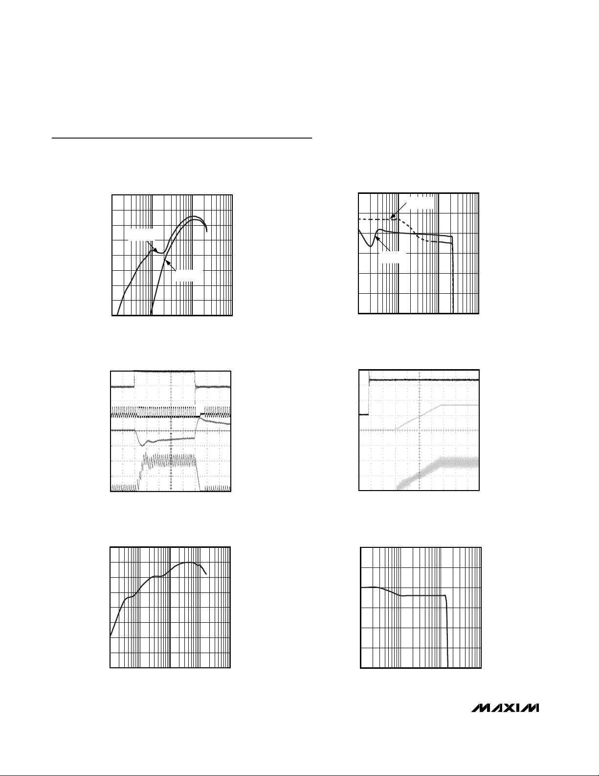
Typical Operating Characteristics
(Circuit of Figure 1. VIN= V
INL
= V
SUPP
= 12V, AVDD= 13.5V, V
GON
= 28V, V
GOFF
= -6V, V
OUT1
= 3.3V, FSEL = GND, TA= +25°C,
unless otherwise noted.)
STEP-DOWN REGULATOR EFFICIENCY
vs. LOAD CURRENT
LOAD CURRENT (A)
EFFICIENCY (%)
MAX8728 toc01
50
55
60
65
70
75
80
85
90
0.01 0.1 1 10
EN = GND
EN = VL
NORMALIZED STEP-DOWN REGULATOR
OUTPUT VOLTAGE vs. LOAD CURRENT
LOAD CURRENT (A)
OUTPUT VOLTAGE (V)
MAX8728 toc02
3.10
3.15
3.20
3.25
3.30
3.35
3.40
0.01 0.1 1 10
EN = GND
EN = VL
STEP-DOWN REGULATOR
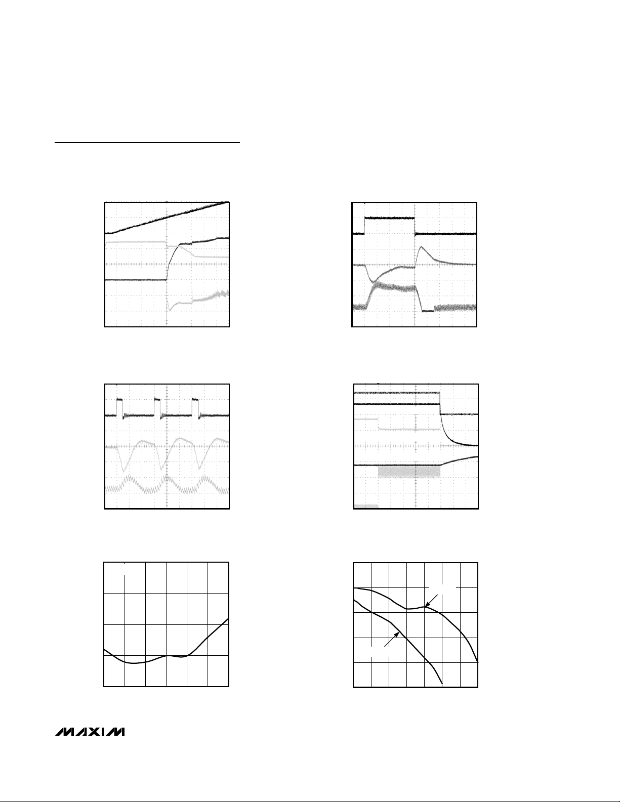
LOAD TRANSIENT RESPONSE
MAX8728toc03
0V
0V
0V
LOAD CONTROL, 5V/div
LX1, 20V/div
OUT1, AC, 100mV/div
INDUCTOR CURRENT, 1A/div
4μs/div
STEP-DOWN REGULATOR
SOFT-START (HEAVY LOAD)
MAX8728toc04
0V
0V
0V
V
IN
, 5V/div
OUT1, 2V/div
INDUCTOR CURRENT, 1A/div
400μs/div
STEP-UP REGULATOR EFFICIENCY
vs. LOAD CURRENT (MEASURED AT L1/C3 JUNCTION)
LOAD CURRENT (A)
EFFICIENCY (%)
MAX8728 toc05
60
65
70
75
80
85
90
95
100
0.001 0.01 0.1 1 10
NORMALIZED STEP-UP REGULATOR
OUTPUT VOLTAGE vs. LOAD CURRENT
LOAD CURRENT (A)
OUTPUT VOLTAGE (V)
MAX8728 toc06
13.30
13.35
13.40
13.45
13.50
13.55
13.60
0.01 0.1 1 10
Page 9
MAX8728
Low-Cost, Multiple-Output
Power Supply for LCD Monitors/TVs
_______________________________________________________________________________________ 9
Typical Operating Characteristics (continued)
(Circuit of Figure 1. VIN= V
INL
= V
SUPP
= 12V, AVDD= 13.5V, V
GON
= 28V, V
GOFF
= -6V, V
OUT1
= 3.3V, FSEL = GND, TA= +25°C,
unless otherwise noted.)
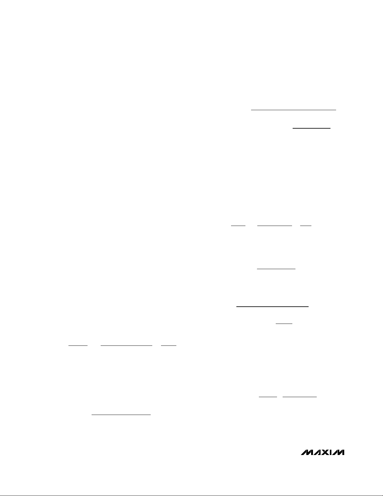
STEP-UP REGULATOR
SOFT-START (HEAVY LOAD)
MAX8728toc07
0V
0V
0V
EN, 2V/div
INDUCTOR CURRENT,
500mA/div
1ms/div
AVDD, 5V/div
GATE, 5V/div
STEP-UP REGULATOR LOAD TRANSIENT
RESPONSE (100mA TO 600mA)
MAX8728toc08
0V
0V
LOAD CONTROL,
5V/div
INDUCTOR CURRENT,
500mA/div
AV
DD
, AC,
200mV/div
10μs/div
STEP-UP REGULATOR PULSED-LOAD
TRANSIENT RESPONSE (100mA TO 1A)
MAX8728toc09
0V
0V
LOAD CONTROL,
5V/div
INDUCTOR CURRENT,
500mA/div
AV
DD
, AC,
100mV/div
4μs/div
TIMER-DELAY
OVERCURRENT PROTECTION
MAX8728toc10
0V
VGON, 20V/div,
10kΩ LOAD
INDUCTOR CURRENT,
1A/div
10ms/div
V
GOFF
, 5V/div, AVDD, 10kΩ LOAD
OUT1, 2V/div, 2.5A OVERLOAD
AVDD, 5V/div, 150Ω LOAD
SWITCHING FREQUENCY
vs. INPUT VOLTAGE
INPUT VOLTAGE (V)
SWITCHING FREQUENCY (MHz)
MAX8728 toc11
7 8 9 10 11 12 13
1.500
1.505
1.510
1.515
1.520
FSEL = GND
NORMALIZED VL OUTPUT VOLTAGE
vs. VL CURRENT
VL CURRENT (mA)
VL VOLTAGE (V)
MAX8728 toc12
0 10203040506070
4.80
4.85
4.90
4.95
5.00
5.05
EN = GND
EN = VL
Page 10

Typical Operating Characteristics (continued)
(Circuit of Figure 1. VIN= V
INL
= V
SUPP
= 12V, AVDD= 13.5V, V
GON
= 28V, V
GOFF
= -6V, V
OUT1
= 3.3V, FSEL = GND, TA= +25°C,
unless otherwise noted.)
MAX8728
Low-Cost, Multiple-Output
Power Supply for LCD Monitors/TVs
10 ______________________________________________________________________________________
POSITIVE CHARGE-PUMP
LOAD TRANSIENT RESPONSE
MAX8728toc16
SRC, AC,
200mV/div
I
SRC
,
20mA/div
40μs/div
NEGATIVE CHARGE-PUMP OUTPUT VOLTAGE
ERROR vs. INPUT VOLTAGE (V
OUT
= -6V)
INPUT VOLTAGE (V)
OUTPUT VOLTAGE ERROR (%)
MAX8728 toc17
7 8 9 10111213
-5
-4
-3
-2
-1
0
1
2
I
OUT
= 10mA
I
OUT
= 100mA
NEGATIVE CHARGE-PUMP
OUTPUT VOLTAGE ERROR vs. LOAD CURRENT
LOAD CURRENT (A)
OUTPUT VOLTAGE ERROR (%)
MAX8728 toc18
-3.0
-2.5
-2.0
-1.5
-1.0
-0.5
0
0.5
1.0
0.001 0.01 0.1 1
REF VOLTAGE vs. REF CURRENT
REF CURRENT (μA)
REF VOLTAGE (V)
MAX8728 toc13
0 20406080100
1.994
1.995
1.996
1.997
1.998
1.999
2.000
POSITIVE CHARGE-PUMP OUTPUT VOLTAGE
ERROR vs. INPUT VOLTAGE (V
OUT
= 28V)
INPUT VOLTAGE (V)
OUTPUT VOLTAGE ERROR (%)
MAX8728 toc14
10.0 10.5 11.0 11.5 12.0 12.5 13.0 13.5
-3.0
-2.5
-2.0
-1.5
-1.0
-0.5
0
0.5
1.0
I
OUT
= 10mA
I
OUT
= 50mA
POSITIVE CHARGE-PUMP OUTPUT
VOLTAGE ERROR vs. LOAD CURRENT
LOAD CURRENT (A)
OUTPUT VOLTAGE ERROR (%)
MAX???? toc15
-3.0
-2.5
-2.0
-1.5
-1.0
-0.5
0
0.5
1.0
0.001 0.01 0.1
Page 11

Typical Operating Characteristics (continued)
(Circuit of Figure 1. VIN= V
INL
= V
SUPP
= 12V, AVDD= 13.5V, V
GON
= 28V, V
GOFF
= -6V, V
OUT1
= 3.3V, FSEL = GND, TA= +25°C,
unless otherwise noted.)
MAX8728
Low-Cost, Multiple-Output
Power Supply for LCD Monitors/TVs
______________________________________________________________________________________ 11
NEGATIVE CHARGE-PUMP
LOAD TRANSIENT RESPONSE
MAX8728toc19
V
GOFF
, AC,
50mV/div
I
VGOFF
,
50mA/div
40μs/div
POWER-UP SEQUENCE
MAX8728toc20
2ms/div
DEL,
C
DEL
= 0.01μF
2V/div
V
GON
, 20V/div, 10kΩ LOAD
V
GOFF
, 5V/div,
10kΩ LOAD
EN, C
EN
= 0.01μF,
2V/div
AV
DD
, 5V/div, 150Ω LOAD
OUT1, 5V/div,
100Ω LOAD
INL SUPPLY CURRENT vs. INL VOLTAGE
INL VOLTAGE (V)
INL SUPPLY CURRENT (mA)
MAX8728 toc21
7 8 9 10111213
0
2
4
6
8
10
EN = GND
EN = GND
INL SUPPLY CURRENT vs. TEMPERATURE
TEMPERATURE (°C)
INL SUPPLY CURRENT (mA)
MAX87228 toc22
-40 -15 10 35 60 85
0
1
2
3
4
5
6
7
EN = VL
EN = GND
HIGH-VOLTAGE SWITCH
CONTROL (MODE 1)
MAX8728toc23
2μs/div
V
CTL
, 5V/div
0V
0V
0V
V
MODE
, 2V/div
V
GON
, 10V/div
HIGH-VOLTAGE SWITCH
CONTROL (MODE 2)
MAX8728toc23
2μs/div
V
CTL
, 5V/div
0V
0V
0V
V
MODE
, 2V/div
V
GON
, 10V/div
Page 12

MAX8728
Low-Cost, Multiple-Output
Power Supply for LCD Monitors/TVs
12 ______________________________________________________________________________________
Pin Description
PIN
FUNCTION
1
Step-Down Regulator and Negative Charge-Pump Power Ground
2
Step-Down Regulator Output Sense Input. OUT1 is the inverting input to the internal current-sense amplifier.
Connect OUT1 directly to the step-down regulator output.
3
Negative Charge-Pump Regulator Driver Output. See the Negative Charge-Pump Regulator section for details.
4 CTL
High-Voltage Switch-Control Block Timing Control Input. See the High-Voltage Switch Control section for
5 IN Step-Down Regulator and Negative Charge-Pump Regulator Supply Input
6 LX1
Step-Down Regulator Switching Node. LX1 is the source of the internal high-side MOSFET. Connect the
inductor and Schottky catch diode to LX1 and minimize the trace area for low EMI.
7 BST
Step-Down Regulator Bootstrap Pin. BST is the supply for the high-side MOSFET gate driver. Connect a 0.1µF
ceramic capacitor from BST to LX1.
8 INL
5V Internal Linear Regulator and Startup Circuitry Supply Input. The input voltage range of INL is between
+7.0V and +13.2V. Connect a 0.22µF ceramic capacitor between INL and GND. Place the capacitor close to
the IC.
9VL
5V Internal Linear Regulator Output. VL powers the internal MOSFET gate drivers and the control circuitry.
Bypass VL
to GND with a 1µF ceramic capacitor. VL can provide up to 25mA external load current.
10 V
CC
Internal Reference Supply Input. Connect VCC directly to VL.
11
Active-Low Shutdown Control Input. All outputs (except for REF and VL) are disabled and the GATE pin goes
high when SHDN is low.
12
Analog Ground
13 REF
Reference Output. Connect a 0.22µF ceramic capacitor between REF and GND. All regulator outputs are
disabled until REF exceeds its UVLO threshold.
14 FBP
Positive Charge-Pump Regulator Feedback Input. Connect FBP to the center of a resistive voltage-divider
between the positive output and GND to set the positive charge-pump regulator output voltage. Place the
resistive voltage-divider close to FBP.
15
Positive Charge-Pump Power Ground
16
Positive Charge-Pump Regulator Driver Output. See the Positive Charge-Pump Regulator section for details.
17
Positive Charge-Pump Regulator Supply Input. Connect SUPP directly to IN and bypass SUPP to GNDP with a
minimum 0.1µF ceramic capacitor.
18
Frequency Select Pin. Connect FSEL to REF for 500kHz operation. Connect FSEL to VCC for 1MHz operation.
Connect to GND for 1.5MHz operation.
19 SRC High-Voltage Switch Control Block Input. SRC is the source of the internal, high-voltage, p-channel MOSFET.
20
High-Voltage Switch Control Block Output. GON is the common junction of the internal high-voltage MOSFETs.
GON is internally pulled to GND through a 4mA internal current source when the switch control block is
disabled.
NAME
GND1
OUT1
DRVN
SHDN
GND
GNDP
DRVP
SUPP
FSEL
GON
Page 13

MAX8728
Low-Cost, Multiple-Output
Power Supply for LCD Monitors/TVs
______________________________________________________________________________________ 13
Pin Description (continued)
PIN
NAME
FUNCTION
21 DRN
High-Voltage Switch Control Input. DRN is the drain of the internal high-voltage p-channel MOSFET connected
to GON. See the High-Voltage Switch Control section for details.
22 THR
GON Falling Regulation Adjustment Input. Connect THR to the center of a resistive voltage-divider between a
reference supply and GND to adjust the GON falling regulation set point. CTL and MODE allow GON to
disconnect from SRC and be discharged through DRN; discharge stops when GON reaches 10 x V
THR
. See
the High-Voltage Switch Control section for details.
23 FB2
Step-Up Regulator Feedback Input. Connect FB2 to the center of a resistive voltage-divider between the stepup regulator output and GND to set the step-up regulator output voltage. Place the resistive voltage-divider
close to FB2.
24 FBN
Negative Charge-Pump Regulator Feedback Input. Connect FBN to the center of a resistive voltage-divider
between the negative output and REF to set the negative charge-pump regulator output voltage. Place the
resistive voltage-divider close to FBN.
25
Step-Down Regulator Power Ground
26 LX2
Step-Up Regulator Switching Node. Connect the inductor and the Schottky diode to LX2 and minimize the
trace area for low EMI.
27
Input MOSFET Gate-Driver Output. GATE controls an external p-channel MOSFET between the input voltage
and the step-up regulator’s inductor. The switch is off when the step-up regulator is turned off, so that the
regulator’s output discharges to ground. During startup, the step-up regulator’s soft-start begins when V
GATE
falls below the GATE done threshold.
28 EN
Enable Input. Pulling EN high or leaving EN unconnected enables the step-up regulator and the negative
charge pump. Connecting EN to GND disables the above blocks and puts the step-down regulator in skip
mode. EN sources 5µA to allow a capacitor-controlled startup delay.
29
High-Voltage Switch-Control Block Mode Selection Input and Timing-Adjustment Input. See the High-Voltage
Switch Control section for details.
30 DEL
Positive Charge-Pump Regulator and High-Voltage Switch-Control Delay Input. Connect a capacitor between
DEL and GND to set the delay time. A 5µA current source charges C
DEL
. DEL is internally pulled to GND
through a 20Ω internal resistor in shutdown.
31
Step-Up Regulator Error Amplifier Compensation Pin. See the Loop Compensation section for details.
32 FB1
Step-Down Regulator Feedback Input. Connect FB1 to the center of a resistive voltage-divider between the
step-down regulator output and GND to set the step-down regulator output voltage.
—EP
Exposed Pad. Connect the exposed backside pad to GND and provide adequate thermal path to cool the IC.
See the PC Board Layout and Grounding section.
GND2
GATE
MODE
COMP
Page 14

MAX8728
Low-Cost, Multiple-Output
Power Supply for LCD Monitors/TVs
14 ______________________________________________________________________________________
MAX8728
AV
DD
13.5V/500mA
GATE
P1
D1
D6
INL
V
IN
10.8V TO 13.2V
OUT1
3.3V/2A
V
GOFF
-6V/150mA
D5
D4
IN
26
25
23
31
4
22
29
21
20
19
14
15
LX1
OUT1
FB1
EN
SHDN
GND1
GND
FBP
GNDP
SRC
REF
GON
DRN
MODE
THR
COMP
C1
10μF
16V
C9
22μF
6.3V
C2
0.22μF
L1
6.4μH
C3
10μF
16V
C24
1000pF
C4
10μF
16V
C7
1μF
C10
0.1μF
R9
44.2kΩ
1%
R10
158kΩ
1%
R3
160kΩ
R4
127kΩ
1%
R5
22.1kΩ
1%
R12
10.0kΩ,
1%
R11
6.49kΩ,1%
R6
2kΩ
R1
115kΩ
1%
R2
20kΩ
1%
R7
287kΩ
1%
R8
22.1kΩ
1%
FROM
TCON
CTL
FB2
LX2
5
8
VLV
CC
L2
2.6μH
910 27
7
6
1
2
32
11
28
DEL
C11
0.1μF
C12
0.22μF
C25
47pF
C14
220pF
C15
1μF
C28
10pF
C13
100pF
C16
0.1μF
C17
1μF
C21
0.1μF
C20
0.1μF
C18
0.1μF
C19
0.1μF
30
13
12
24
3
18
17 16
D2
C8
0.1μF
C5
10μF
16V
C6
10μF
16V
GND2
FBN
DRVN
SUPPFSEL
DRVP
BST
V
GON
28V/50mA
ON/OFF
D3
VIN
Figure 1. Typical Operating Circuit
Page 15

MAX8728
Low-Cost, Multiple-Output
Power Supply for LCD Monitors/TVs
______________________________________________________________________________________ 15
Typical Operating Circuit
The typical operating circuit (Figure 1) of the MAX8728 is
a complete power-supply system for TFT LCD panels in
monitors and TVs. The circuit generates a +3.3V logic
supply, a +13.5V source driver supply, a +28V positive
gate driver supply, and a -6V negative gate driver supply
from a 12V ±10% input supply and operates at 1.5MHz.
Table 1 lists some selected components and Table 2
lists the contact information for component suppliers.
Detailed Description
The MAX8728 is a multiple-output power supply
designed primarily for TFT LCD panels used in monitors
and TVs. It contains a step-down switching regulator to
generate the logic supply rail, a step-up switching regulator to generate the source driver supply, and two
charge-pump regulators to generate the gate-driver
supplies. Each regulator features adjustable output voltage, digital soft-start, and timer-delayed fault protection.
Both the step-down and step-up regulators use fixedfrequency current-mode control architectures. The two
switching regulators are 180° out of phase to minimize
the input ripple. The internal oscillator offers three pinselectable frequency options (500kHz/1MHz/1.5MHz)
allowing users to optimize their designs based on the
specific application requirements. In addition, the
MAX8728 features a high-voltage switch-control block,
an internal 5V linear regulator, a 2V reference output,
well-defined power-up and power-down sequences,
and thermal-overload protection. Figure 2 shows the
MAX8728 functional diagram.
Step-Down Regulator
The step-down regulator consists of an internal n-channel MOSFET with gate driver, a lossless current-sense
network, a current-limit comparator, and a PWM controller block. The external power stage consists of a
Schottky diode rectifier, an inductor, and output capacitors. The output voltage is regulated by changing the
duty cycle of the high-side MOSFET. A bootstrap circuit
that uses a 0.1µF flying capacitor between LX1 and
BST provides the supply voltage for the high-side gate
driver. Although the MAX8728 also includes a 25Ω (typ)
low-side MOSFET, this switch is used to charge the
bootstrap capacitor during startup and maintains fixedfrequency operation at light load and cannot be used
as a synchronous rectifier. An external Schottky diode
(D2 in Figure 1) is always required.
PWM Controller Block
The heart of the PWM control block is a multi-input,
open-loop comparator that sums three signals: the out-
put voltage signal with respect to the reference voltage,
the current-sense signal, and the slope compensation.
The PWM controller is a direct-summing type, lacking a
traditional error amplifier and the phase shift associated
with it. This direct-summing configuration approaches
ideal cycle-by-cycle control over the output voltage.
When EN is high or floating, the controller always operates in fixed-frequency PWM mode. Each pulse from
the oscillator sets the main PWM latch that turns on the
high-side switch until the PWM comparator changes
state. As the high-side switch turns off, the low-side
switch turns on. The low-side switch stays on until the
beginning of the next clock cycle.
When EN is low, the controller operates in skip mode.
The skip mode dramatically improves light-load efficiency by reducing the effective frequency, which
reduces switching losses. It keeps the actual peak
inductor current at about 0.8A in an active cycle, allowing subsequent cycles to be skipped. Skip mode transitions seamlessly to fixed-frequency PWM operation as
load current increases.
Table 1. Component List (1.5MHz)
DESIGNATION DESCRIPTION
C1, C3, C4, C5, C6
10µF ±20%, 16V X5R ceramic
capacitors (1206)
TDK C3216X5R1C106M
D1, D2
3A, 30V Schottky diode (M-flat)
Toshiba CMS02 (top mark S2)
D3, D4, D5
220mA, 100V dual diode (SOT23)
Fairchild MMBD4148SE (top mark D4)
L1
6.4µH, 1.5ADC inductor
Sumida CDRH6D12-6R4
L2
2.6µH, 2.6ADC inductor
Sumida CDRH6D12-2R6
P1
2.4A, -20V p-channel MOSFET
(3-pin SuperSOT)
Fairchild FDN304P (top mark 304)
Table 2. Component Suppliers
SUPPLIER PHONE
Fairchild Semiconductor 408-822-2000
Sumida 847-545-6700
TDK 847-803-6100
Toshiba 949-455-2000
Page 16

MAX8728
Low-Cost, Multiple-Output
Power Supply for LCD Monitors/TVs
16 ______________________________________________________________________________________
V
L
IN
BST
GATEINL
LX2
GND2
FB2
COMP
LX1
GND1
OUT1
FB1
SHDN
EN
DEL
REF
GND
FBN
FSEL
DRVN
SUPP
CTL
THR
MODE
DRN
GON
SRC
FBP
DRVP
V
IN
OUT1
V
CC
V
L
V
L
V
GOFF
AV
DD
V
GON
FROM TCON
ON/OFF
LCD ENABLE
IN
STEP-DOWN
REGULATOR
SEQUENCE
CONTROL
V
L
REGULATOR
STEP-UP
REGULATOR
THERMAL
SHUTDOWN
OSCILLATOR
FAULT
LOGIC AND
TIMER
REFERENCE
NEGATIVE
REGULATOR
SWITCH
CONTROL
BLOCK
POSITIVE
REGULATOR
MAX8728
VIN
Figure 2. Functional Diagram
Page 17

MAX8728
Low-Cost, Multiple-Output
Power Supply for LCD Monitors/TVs
______________________________________________________________________________________ 17
Current Limiting and Lossless Current Sensing
The current-limit circuit turns off the high-side MOSFET
switch whenever the voltage across the high-side
MOSFET exceeds an internal threshold corresponding to
the actual current limit of 2.8A ±10%.
For current-mode control, an internal lossless sense
network derives a current-sense signal from the inductor DC resistance. The time constant of the currentsense network is not required to match the time
constant of the inductor and has been chosen to provide sufficient current-ramp signal for stable operation
at each operating frequency. The current-sense signal
is AC-coupled into the PWM comparator, eliminating
most DC output voltage variation with load current.
Low-Frequency Operation
The step-down regulator of the MAX8728 enters into
low-frequency operating mode if the voltage on OUT1
is below 1.3V. In the low-frequency mode, the switching
frequency of the step-down regulator is 1/6 the oscillator frequency. This feature prevents potentially uncontrolled inductor current if OUT1 is overloaded or
shorted to ground.
Soft-Start and Fault Protection
The step-down regulator includes a 7-bit soft-start DAC
that steps the internal reference voltage from zero to 2V
in 128 steps. The soft-start period is 3ms (typ) and FB1
fault detection is disabled during this period. The softstart feature effectively limits the inrush current during
startup (see the Step-Down Regulator Soft-Start
Waveforms in the Typical Operating Characteristics).
The MAX8728 monitors OUT1 (fixed-output mode) or
FB1 (adjustable-output mode) for undervoltage conditions. If the voltage is continuously below 80% (typ) of
the nominal regulation point for approximately 50ms,
the MAX8728 sets a fault latch, shutting down all outputs except VL and REF.
Step-Up Regulator
The step-up regulator employs a current-mode, fixedfrequency PWM architecture to maximize loop bandwidth and provide fast transient response to pulsed
loads typical of TFT LCD panel source drivers. The integrated MOSFET and the built-in digital soft-start function
reduce the number of external components required
while controlling inrush currents. The output voltage can
be set from VINto 28V with an external resistive voltagedivider. The regulator controls the output voltage and
the power delivered to the output by modulating the
duty cycle of the internal power MOSFET in each
switching cycle.
PWM Controller Block
An error amplifier compares the signal at FB2 to 2.0V
and changes the COMP output. The voltage at COMP
sets the peak inductor current. As the load varies, the
error amplifier sources or sinks current to the COMP
output accordingly to produce the inductor peak current necessary to service the load. To maintain stability
at high duty cycles, a slope-compensation signal is
summed with the current-sense signal.
On the rising edge of the internal clock, the controller
sets a flip-flop, turning on the n-channel MOSFET and
applying the input voltage across the inductor. The current through the inductor ramps up linearly, storing
energy in its magnetic field. Once the sum of the current-feedback signal and the slope compensation
exceed the COMP voltage, the controller resets the flipflop and turns off the MOSFET. Since the inductor current is continuous, a transverse potential develops
across the inductor that turns on the diode (D1). The
voltage across the inductor then becomes the difference between the output voltage and the input voltage.
This discharge condition forces the current through the
inductor to ramp back down, transferring the energy
stored in the magnetic field to the output capacitor and
the load. The MOSFET remains off for the rest of the
clock cycle.
Input Switch Control
The GATE pin of the MAX8728 controls an optional
external p-channel MOSFET between the input supply
and the inductor of the step-up regulator. This function
disconnects the step-up regulator from the input supply
and allows the regulator output to discharge to ground
when the step-up regulator is disabled. When EN is low,
GATE is internally pulled up to the input supply through
a 1kΩ resistor. Once EN and SHDN are high and the
negative charge-pump regulator is in regulation, the
MAX8728 starts pulling down GATE with an 11µA internal current source. The external p-channel MOSFET
turns on and connects the input supply to the step-regulator when V
GATE
falls below the turn-on threshold of the
MOSFET. When V
GATE
reaches VIN- 4V, the step-up
regulator is enabled and initiates a soft-start routine.
V
GATE
continues to fall until it reaches VIN- 5V.
Soft-Start and Fault Protection
The step-up regulator achieves soft-start by linearly
ramping up its internal current limit. The soft-start terminates when the output reaches regulation or the full
current limit has been reached. The current limit rises
from zero to the full current limit in approximately 3ms.
Page 18

MAX8728
Low-Cost, Multiple-Output
Power Supply for LCD Monitors/TVs
18 ______________________________________________________________________________________
The soft-start feature effectively limits the inrush current
during startup (see the Step-Up Regulator Soft-Start
Waveforms in the Typical Operating Characteristics).
The MAX8728 monitors FB2 for undervoltage conditions. If the voltage is continuously below 90% of the
nominal regulation point for approximately 50ms, the
MAX8728 sets a fault latch, shutting down all outputs
except VL, REF, and the step-down regulator.
Positive Charge-Pump Regulator
The positive charge-pump regulator is typically used to
generate the positive supply rail for the TFT LCD gatedriver ICs. The output voltage is set with an external
resistive voltage-divider from its output to GND with the
midpoint connected to FBP. The number of chargepump stages and the setting of the feedback divider
determine the output voltage of the positive chargepump regulator. The charge pump includes a highside, p-channel MOSFET (P1) and a low-side,
n-channel MOSFET (N1) to control the power transfer
as shown in Figure 3.
The error comparator compares the feedback signal
(FBP) with a 2.0V internal reference. If the feedback
signal is below the reference, the charge-pump regulator turns on P1 and turns off N1 when the rising edge of
the oscillator clock arrives, level shifting the flying
capacitors (C18 and C19) by V
SUPP
volts. If the result-
ing voltage on C18 and C19 is greater than their asso-
ciated reservoir capacitors (C20 and C15), charge
flows until the diode connecting each flying capacitor
to its reservoir capacitor turns off. The falling edge of the
oscillator clock turns off P1 and turns on N1, charging
the flying capacitors (C18 and C19) through the diodes
that connect them to the reservoir capacitors (C21 and
C20). If the feedback signal is above the reference
when the rising edge of the oscillator comes, the regulator ignores this clock edge and keeps N1 on and P1 off.
The positive charge-pump regulator’s startup can be
delayed by connecting an external capacitor from DEL to
GND. An internal constant-current source begins charging the DEL capacitor when EN and SHDN are logic high,
the negative charge pump reaches regulation, and GATE
has gone low. When the DEL voltage exceeds V
REF
/2,
the positive charge-pump regulator is enabled. Each time
it is enabled, the positive charge-pump regulator goes
through a soft-start routine by ramping up its internal reference voltage from 0 to 2V in 128 steps. The soft-start
period is 3ms (typ) and FBP fault detection is disabled
during this period. The soft-start feature effectively limits
the inrush current during startup. The MAX8728 also
monitors the FBP voltage for undervoltage conditions. If
VFBP is continuously below 80% of its nominal regulation
point for approximately 50ms, the MAX8728 sets a fault
latch, shutting down all outputs except VL, REF, and the
step-down regulator.
LEVEL
SHIFT
REF
Q
CLK
D
OSC
FF
ERROR
COMPARATOR
P1
N1
DRVP
C21
C20
C15
C28
C19
C18
GNDP
SUPP
FBP
POSITIVE CHARGE-PUMP REGULATOR
INPUT
SUPPLY
OUTPUT
MAX8728
Figure 3. Positive Charge-Pump Regulator Block Diagram
Page 19

MAX8728
Low-Cost, Multiple-Output
Power Supply for LCD Monitors/TVs
______________________________________________________________________________________ 19
Negative Charge-Pump Regulator
The negative charge-pump regulator is typically used to
generate the negative supply rail for the TFT LCD gatedriver ICs. The output voltage is set with an external
resistive voltage-divider from its output to REF with the
midpoint connected to FBN. The number of chargepump stages and the setting of the feedback-divider
determine the output of the negative charge-pump regulator. The charge-pump controller includes a high-side,
p-channel MOSFET (P2) and a low-side, n-channel
MOSFET (N2) to control the power transfer as shown in
Figure 4.
The error comparator compares the feedback signal
(FBN) with a 250mV internal reference. If the feedback
signal is above the reference, the charge-pump regulator turns on N2 and turns off P2 when the rising edge of
the oscillator clock arrives, level shifting the flying
capacitor (C16). The falling edge of the oscillator clock
turns off N2 and turns on P2, charging the flying capacitor (C16) through the diode that connects it to the
reservoir capacitor (C1). If the feedback signal is below
the reference (output is in regulation) when the rising
edge of the oscillator comes, the regulator ignores this
clock edge and keeps P2 on and N2 off.
The negative charge-pump regulator is enabled when
SHDN and EN are logic high and the step-down regulator reaches regulation. Each time it is enabled, the negative charge-pump regulator goes through a soft-start
routine by ramping down its internal reference voltage
from 2V to 250mV in 128 steps. The soft-start period is
3ms (typ) and FBN fault detection is disabled during
this period. The soft-start feature effectively limits the
inrush current during startup. The MAX8728 also monitors the FBN voltage for undervoltage conditions. If
V
FBN
is continuously above 600mV for approximately
50ms, the MAX8728 sets a fault latch, shutting down all
outputs except VL, REF, and the step-down regulator.
High-Voltage Switch Control
The MAX8728’s high-voltage switch control block
(Figure 5) consists of two high-voltage, p-channel
MOSFETs: Q1, between SRC and GON and Q2,
between GON and DRN. The switch control block is
enabled when V
DEL
goes above V
REF
/ 2. Q1 and Q2
are controlled by CTL and MODE. There are two different modes of operation (see the Typical Operating
Characteristics section).
Activate the first mode by connecting MODE to REF.
When CTL is logic high, Q1 turns on and Q2 turns off,
connecting GON to SRC. When CTL is logic low, Q1
0.25V
Q
CLK
D
OSC
FF
ERROR
COMPARATOR
P2
N2
DRVN
GND1
IN
FBN
NEGATIVE CHARGE-PUMP REGULATOR
INPUT
SUPPLY
OUTPUT
REF
MAX8728
C17
C16
C1
Figure 4. Negative Charge-Pump Regulator Block Diagram
Page 20

MAX8728
Low-Cost, Multiple-Output
Power Supply for LCD Monitors/TVs
20 ______________________________________________________________________________________
turns off and Q2 turns on, connecting GON to DRN.
GON can then be discharged through a resistor connected between DRN and GND or AVDD. Q2 turns off
and stops discharging GON when V
GON
reaches 10
times the voltage on THR.
When V
MODE
is less than 0.9 x V
REF
, the switch control
block works in the second mode. The rising edge of
V
CTL
turns on Q1 and turns off Q2, connecting GON to
SRC. An internal n-channel MOSFET Q3 between
MODE and GND is also turned on to discharge an
external capacitor between MODE and GND. The
falling edge of VCTL turns off Q3, and an internal 50µA
current source starts charging the MODE capacitor.
Once V
MODE
exceeds 0.5 x V
REF
, the switch control
block turns off Q1 and turns on Q2, connecting GON to
DRN. GON can then be discharged through a resistor
connected between DRN and GND or AVDD. Q2 turns
off and stops discharging GON when V
GON
reaches 10
times the voltage on THR.
When the LCD is shut down or in a fault state, the
switch control block is disabled, DZL is held low, and
GON is discharged to GND through an internal 4mA
current source. If the DRN resistor connects DRN to
AVDDor another voltage above ground, the Q2 body
diode conducts. To prevent the body diode conduction, an external diode must be added in series with the
DRN resistor (D6 in Figure 1). During startup, the 4mA
current source and Q4 are released when GATE reaches the GATE DONE threshold.
Linear Regulator (VL)
The MAX8728 includes an internal linear regulator. INL
is the input of the linear regulator. The input voltage
range is between 7V and 13.2V. The output voltage is
set to 5V. The regulator powers the internal MOSFET
drivers, PWM controllers, charge-pump regulators, and
logic circuitry. The total external load capability is
25mA. Bypass VL to GND with a minimum 1µF ceramic
capacitor.
Reference Voltage (REF)
The reference output is nominally 2V, and can
source at least 50µA (see the Typical Operating
Characteristics section). VCCis the input of the internal
reference block. Bypass REF with a 0.22µF ceramic
capacitor connected between REF and GND.
Frequency Selection (FSEL)
The step-down regulator and step-up regulator use the
same internal oscillator. The FSEL input selects the
switching frequency. Table 3 shows the switching frequency based on the FSEL connection. High-frequency
(1.5MHz) operation optimizes the application for the
smallest component size, trading off efficiency due to
higher switching losses. Low-frequency (500kHz) operation offers the best overall efficiency at the expense of
component size and board space.
To reduce the input RMS current, the step-down regulator and the step-up regulator operate 180° out of
phase from each other. The feature allows the use of
less input capacitance.
Power-Up Sequence
The step-down regulator starts up when the MAX8728’s
internal reference voltage (REF) is above its undervoltage lockout (UVLO) threshold and SHDN is logic high.
The FB1 fault-detection circuit is enabled after the stepdown regulator reaches regulation. The negative
charge-pump regulator starts up when both EN and
SHDN are logic high and REF is above its UVLO threshold. Once the negative charge-pump regulator output is
in regulation, the MAX8728 enables the FBN fault-detection circuit and the input-switch control block, which starts
pulling down GATE with a 11µA internal current source.
The external p-channel MOSFET turns on and connects
the input supply to the step-up regulator when V
GATE
falls below the turn-on threshold of the MOSFET.
When V
GATE
reaches the GATE DONE threshold, the
MAX8728 enables the step-up regulator and the positive charge-pump adjustable delay block. The FB2
fault-detection circuit is enabled after the step-up regulator reaches regulation. The delay block charges the
DEL capacitor with an internal 5µA current source and
V
DEL
rises linearly. When V
DEL
exceeds 1V (typ), the
MAX8728 enables the positive charge-pump regulator
and the high-voltage switch control block. The FBP fault
detection is enabled after the positive charge-pump
regulator reaches regulation.
Power-Down Control
The MAX8728 disables the step-up regulator, positive
charge-pump regulator, negative charge-pump regulator, input switch control block, delay block, and highvoltage switch control block when EN or SHDN is logic
low, or when any fault latch is set. The step-down regulator is disabled only when SHDN is logic low, the stepdown fault latch is set, or during thermal overload.
Table 3. Frequency Selection
FSEL
SWITCHING FREQUENCY (kHz)
GND 1500
VCC 1000
REF 500
Page 21

MAX8728
Low-Cost, Multiple-Output
Power Supply for LCD Monitors/TVs
______________________________________________________________________________________ 21
MODE
CTL
DEL
SRC
GON
DRN
0.5 x V
REF
GATE DONE
5μA
REF
Q1
4mA
Q4
Q3
R
4R
5R
50μA
SWITCH CONTROL
THR
9R
1kΩ
R
REF
1kΩ
SHDN
FAULT
EN
MAX8728
Q2
Figure 5. Switch-Control Functional Diagram
Page 22

MAX8728
Low-Cost, Multiple-Output
Power Supply for LCD Monitors/TVs
22 ______________________________________________________________________________________
Fault Protection
During steady-state operation, if any output of the four
regulators (step-down regulator, step-up regulator,
positive charge-pump regulator, and negative chargepump regulator) does not exceed its respective faultdetection threshold, the MAX8728 activates an internal
fault timer. If any condition or the combination of conditions indicates a continuous fault for the fault-timer
duration (50ms typ), the MAX8728 sets a fault latch. If
the fault is caused by the step-up regulator or one of
the charge pumps (LCD fault), the MAX8728 shuts
down all the outputs except VL, REF, and the stepdown regulator. Once the fault condition is removed,
toggle EN or SHDN, or cycle the input voltage to clear
the LCD fault latch and restart the LCD supplies. If the
fault is caused by the step-down regulator, the
MAX8728 shuts down all the outputs except VL and
REF. Once the fault condition is removed, toggle SHDN
or cycle the input voltage to clear the step-down fault
latch and restart the supplies.
Thermal-Overload Protection
The thermal-overload protection prevents excessive
power dissipation from overheating the MAX8728.
When the junction temperature exceeds TJ= +160°C, a
thermal sensor immediately activates the fault protection, which shuts down all the outputs except the reference, allowing the device to cool down. Once the
device cools down by approximately 15°C, the
MAX8728 automatically restarts all the supplies.
The thermal-overload protection protects the controller
in the event of fault conditions. For continuous operation, do not exceed the absolute maximum junction
temperature rating of TJ= +150°C.
Design Procedure
Step-Down Regulator Design
Inductor Selection
Three key inductor parameters must be specified:
inductance value (L), peak current (I
PEAK
), and DC
resistance (RDC). The following equation includes a
constant, LIR, which is the ratio of peak-to-peak inductor ripple current to DC load current. A higher LIR value
allows smaller inductance, but results in higher losses
and higher ripple. A good compromise between size
and losses is typically found at a 30% ripple-current to
load-current ratio (LIR = 0.3), which corresponds to a
peak inductor current 1.15 times the DC load current:
where I
OUT1(MAX)
is the maximum DC load current, and
the switching frequency fSWis 1.5MHz when FSEL is
tied to GND, 1MHz when FSEL is tied to VCC, and
500kHz when FSEL is tied to REF. The exact inductor
value is not critical and can be adjusted to make tradeoffs among size, cost, and efficiency. Lower inductor
values minimize size and cost, but they also increase
the output ripple and reduce the efficiency due to higher peak currents. On the other hand, higher inductor
values increase efficiency, but at some point resistive
losses due to extra turns of wire will exceed the benefit
gained from lower AC current levels.
The inductor’s saturation current must exceed the peak
inductor current. The peak current can be calculated by:
The inductor’s DC resistance should be low for good
efficiency. Find a low-loss inductor having the lowest
possible DC resistance that fits in the allotted dimensions. Ferrite cores are usually the best choice, especially at the higher frequency settings. Shielded-core
geometries help keep noise, EMI, and switching waveform jitter low.
Input Capacitors
The input filter capacitors reduce peak currents drawn
from the power source and reduce noise and voltage
ripple on the input caused by the regulator’s switching.
They are usually selected according to input ripple current requirements and voltage rating, rather than
capacitance value. The input voltage and load current
determine the RMS input ripple current (I
RMS
):
The worst case is I
RMS
= 0.5 x I
OUT1
, which occurs at
VIN= 2 x V
OUT1
.
For most applications, ceramic capacitors are used
because of their high ripple current and surge-current
capabilities. For optimal circuit long-term reliability,
choose an input capacitor that exhibits less than +10°C
temperature rise at the RMS input current corresponding to the maximum load current.
II
VVV
V
RMS OUT
OUT IN OUT
IN
=×
×−
()
1
11
I
VVV
fL V
II
I
OUT RIPPLE
OUT IN OUT
SW OUT IN
OUT PEAK OUT MAX
OUT RIPPLE
1
11
1
11
1
2
_
_()
_
=
×−
()
××
=+
L
VVV
V f I LIR
OUT
OUT IN OUT
IN SW OUT MAX
1
11
1 ()
=
×−
()
×× ×
Page 23

MAX8728
Low-Cost, Multiple-Output
Power Supply for LCD Monitors/TVs
______________________________________________________________________________________ 23
Output-Capacitor Selection
Since the MAX8728’s step-down regulator is internally
compensated, it is stable with any reasonable amount
of output capacitance. However, the actual capacitance and equivalent series resistance (ESR) affect the
regulator’s output ripple voltage and transient
response. The rest of this section deals with how to
determine the output capacitance and ESR needs
according to the ripple voltage and load-transient
requirements.
The output voltage ripple has two components: variations in the charge stored in the output capacitor, and
the voltage drop across the capacitor’s ESR caused by
the current into and out of the capacitor:
where I
OUT1_RIPPLE
is defined in the Step-Down
Regulator, Inductor Selection section, C
OUT1
is output
capacitance, and R
ESR_OUT1
is the ESR of output
capacitor C
OUT1
. In Figure 1’s circuit, the inductor ripple current is 0.6A. If the voltage ripple requirement of
Figure 1’s circuit is ±1% of the 3.3V output, then the
total peak-to-peak ripple voltage should be less than
66mV. Assuming that the ESR ripple and the capacitive
ripple each should be less than 50% of the total peakto-peak ripple, then the ESR should be less than 55mΩ
and the output capacitance should be more than 1.5µF
to meet the total ripple requirement. A 22µF capacitor
with ESR (including PC board trace resistance) of 10mΩ
is selected for the standard application circuit in Figure 1,
which easily meets the voltage-ripple requirement.
The step-down regulator’s output capacitor and ESR
also affect the voltage undershoot and overshoot when
the load steps up and down abruptly. The undershoot
and overshoot also have two components: the voltage
steps caused by ESR and voltage sag and soar due to
the finite capacitance and inductor slew rate. Use the
following formulae to check if the ESR is low enough
and the output capacitance is large enough to prevent
excessive soar and sag.
The amplitude of the ESR step is a function of the load
step and the ESR of the output capacitor:
V
OUT1_ESR_STEP
= ΔI
OUT1
x R
ESR_OUT1
The amplitude of the capacitive sag is a function of the
load step, the output capacitor value, the inductor
value, the input-to-output voltage differential, and the
maximum duty cycle:
The amplitude of the capacitive soar is a function of the
load step, the output capacitor value, the inductor
value and the output voltage:
Given the component values in the circuit of Figure 1,
during a 2A step-load transient, the voltage step due to
capacitor ESR is negligible. The voltage sag and soar
are 40.2mV and 71.6mV, respectively.
Rectifier Diode
The MAX8728’s high switching frequency demands a
high-speed rectifier. Schottky diodes are recommended
for most applications because of their fast recovery time
and low forward voltage. In general, a 2A Schottky
diode works well in the MAX8728’s step-down regulator.
Output-Voltage Selection
Connect a resistive voltage-divider between OUT1 and
GND with the center tap connected to FB1 to adjust the
output voltage. Choose R12 (resistance from FB1 to
GND) to be between 5kΩ and 50kΩ, and solve for R11
(resistance from OUT1 to FB1) using the equation:
where V
FB1
= 2V, and V
OUT1
may vary from 2V to 3.6V.
Connecting a small capacitor (e.g., 47pF) between FB1
and GND reduces FB1 noise sensitivity.
Step-Up Regulator Design
Inductor Selection
The inductance value, peak-current rating, and series
resistance are factors to consider when selecting the
step-up inductor. These factors influence the converter’s efficiency, maximum output load capability, transient response time, and output voltage ripple. Physical
size and cost are also important factors to be considered.
The maximum output current, input voltage, output voltage, and switching frequency determine the inductor
value. Very high inductance values minimize the cur-
RR
V
V
OUT
FB
11 12 1
1
1
=× −
⎛
⎝
⎜
⎞
⎠
⎟
V
LI
CV
OUT SOAR
OUT OUT
OUT OUT
1
11
2
11
2
_
()
=
×
××
Δ
V
LI
CV DV
OUT SAG
OUT OUT
OUT IN MIN MAX OUT
1
11
2
11
2
_
()
()
=
×
×× ×−
()
Δ
VV V
VIR
V
I
Cf
OUT RIPPLE OUT RIPPLE ESR OUT RIPPLE C
OUT RIPPLE ESR OUT RIPPLE ESR OUT
OUT RIPPLE C
OUT RIPPLE
OUT SW
11 1
11 1
1
1
1
8
__()_()
_() _ _
_()
_
=+
=×
=
××
Page 24
MAX8728
Low-Cost, Multiple-Output
Power Supply for LCD Monitors/TVs
24 ______________________________________________________________________________________
rent ripple and therefore reduce the peak current,
which decreases core losses in the inductor and I2R
losses in the entire power path. However, large inductor values also require more energy storage and more
turns of wire, which increase physical size and can
increase I
2
R losses in the inductor. Low inductance values decrease the physical size but increase the current
ripple and peak current. Finding the best inductor
involves choosing the best compromise between circuit
efficiency, inductor size, and cost.
The equations used here include a constant LIR, which
is the ratio of the inductor peak-to-peak ripple current
to the average DC inductor current at the full load current. The best trade-off between inductor size and circuit efficiency for step-up regulators generally has an
LIR between 0.2 and 0.5. However, depending on the
AC characteristics of the inductor core material and
ratio of inductor resistance to other power-path resistances, the best LIR can shift up or down. If the inductor resistance is relatively high, more ripple can be
accepted to reduce the number of turns required and
increase the wire diameter. If the inductor resistance is
relatively low, increasing inductance to lower the peak
current can decrease losses throughout the power
path. If extremely thin, high-resistance inductors are
used, as is common for LCD panel applications, the
best LIR can increase to between 0.5 and 1.0.
Once a physical inductor is chosen, higher and lower
values of the inductor should be evaluated for efficiency improvements in typical operating regions.
Calculate the approximate inductor value using the typical input voltage (V
IN
), the maximum output current
(I
AVDD(MAX)
), the expected efficiency (η
TYP
) taken from
an appropriate curve in the Typical Operating
Characteristics, and an estimate of LIR based on the
above discussion:
Choose an available inductor value from an appropriate
inductor family. Calculate the maximum DC input current at the minimum input voltage V
IN(MIN)
using con-
servation of energy and the expected efficiency at that
operating point (η
MIN
) taken from an appropriate curve
in the Typical Operating Characteristics:
Calculate the ripple current at that operating point and
the peak current required for the inductor:
The inductor’s saturation current rating and the
MAX8728’s LX2 current limit should exceed I
AVDD_PEAK
and the inductor’s DC current rating should exceed
I
IN(DC,MAX)
. For good efficiency, choose an inductor
with less than 0.1Ω series resistance.
Considering the Typical Operating Circuit in Figure 1,
the maximum load current (I
AVDD(MAX)
) is 500mA with
a 13.5V output and a typical input voltage of 12V.
Choosing an LIR of 0.3 and estimating efficiency of
95% at this operating point:
Using the circuit’s minimum input voltage (10.8V) and
estimating efficiency of 90% at that operating point:
The ripple current and the peak current are:
Output-Capacitor Selection
The total output voltage ripple has two components: the
capacitive ripple caused by the charging and discharging of the output capacitance, and the ohmic ripple due to the capacitor’s ESR:
where I
AVDD_PEAK
is the peak-inductor current (see the
Inductor Selection section). For ceramic capacitors, the
VV V
V
I
C
VV
Vxf
and
VIxR
AVDD RIPPLE AVDD RIPPLE C AVDD RIPPLE ESR
AVDD RIPPLE C
AVDD
AVDD
AVDD IN
AVDD SW
AVDD RIPPLE ESR AVDD PEAK ESR
__()_()
_()
_() _ _
,
=+
≈
−
⎛
⎝
⎜
⎞
⎠
⎟
≈
I
VVV
H V MHz
A
IAAA
RIPPLE
PEAK
. . .
. . .
.
. . .
=
×−
()
××
≈
=+ ≈
10 8 13 5 10 8
6 4 13 5 1 5
023
069
023
2
081
μ
I
AV
V
A
IN DC MAX(, )
. .
. .
.=
×
×
≈
0 5 13 5
10 8 0 9
069
L
V
V
VV
A MHz
H
AVDD
.
.
..
.
.
.=
⎛
⎝
⎜
⎞
⎠
⎟
−
×
⎛
⎝
⎜
⎞
⎠
⎟
⎛
⎝
⎜
⎞
⎠
⎟
≈
12
13 5
13 5 12
05 15
095
05
64
2
μ
I
VVV
LVf
II
I
AVDD RIPPLE
IN MIN AVDD IN MIN
AVDD AVDD SW
AVDD PEAK IN DC MAX
AVDD RIPPLE
_
() ()
_(,)
_
=
×−
()
××
=+
2
I
IV
V
IN DC MAX
AVDD MAX AVDD
IN MIN MIN
(, )
()
()
=
×
×η
L
V
V
VV
I f LIR
AVDD
IN
AVDD
AVDD IN
AVDD MAX SW
TYP
()
=
⎛
⎝
⎜
⎞
⎠
⎟
−
×
⎛
⎝
⎜
⎞
⎠
⎟
⎛
⎝
⎜
⎞
⎠
⎟
2
η
Page 25

MAX8728
Low-Cost, Multiple-Output
Power Supply for LCD Monitors/TVs
______________________________________________________________________________________ 25
output voltage ripple is typically dominated by
V
AVDD_RIPPLE(C)
. The voltage rating and temperature
characteristics of the output capacitor must also be
considered.
Input-Capacitor Selection
The input capacitor reduces the current peaks drawn
from the input supply and reduces noise injection into
the IC. Two 10µF ceramic capacitors are used in the
Typical Applications Circuit (Figure 1) because of the
high-source impedance seen in typical lab setups.
Actual applications usually have much lower source
impedance since the step-up regulator often runs
directly from the output of another regulated supply.
Typically, the input capacitance can be reduced below
the values used in the Typical Operating Circuit.
Rectifier Diode
The MAX8728’s high-switching frequency demands a
high-speed rectifier. Schottky diodes are recommended for most applications because of their fast recovery
time and low forward voltage. In general, a 1A to 2A
Schottky diode complements the internal MOSFET well.
Output-Voltage Selection
The output voltage of the step-up regulator is adjusted
by connecting a resistive voltage-divider from the output (V
AVDD
) to GND with the center tap connected to
FB2 (see Figure 1). Select R2 in the 10kΩ to 50kΩ
range. Calculate R1 with the following equation:
where V
FB2
, the step-up regulator’s feedback set point,
is 2.0V. Place R1 and R2 close to the IC.
Loop Compensation
Choose R
COMP
(R3 in Figure 1) to set the high-frequency integrator gain for fast-transient response. Choose
C
COMP
(C13 in Figure 1) to set the integrator zero to
maintain loop stability.
For low-ESR output capacitors, use the following equations to obtain stable performance and good transient
response:
To further optimize transient response, vary R
COMP
in
20% steps and C
COMP
in 50% steps while observing
transient response waveforms.
Charge-Pump Regulators
Selecting the Number of Charge-Pump Stages
For highest efficiency, always choose the lowest number of charge-pump stages that meet the output
requirement.
The number of positive charge-pump stages is given by:
where n
POS
is the number of positive charge-pump
stages, V
GON
is the output of the positive charge-pump
regulator, I
GON
is the positive charge-pump output cur-
rent, V
SUPP
is the supply voltage of the charge-pump
regulators, V
D
is the forward voltage drop of the
charge-pump diode, and R
EFF
is the effective output
resistance of the charge-pump switches (10Ω typ.)
The number of negative charge-pump stages is given by:
where n
NEG
is the number of negative charge-pump
stages, V
GOFF
is the output of the negative charge-
pump regulator, and I
GOFF
is the negative charge-
pump output current.
The above equations assume that the flying capacitors
are large enough to not further limit the output current.
Flying Capacitors
Increasing the flying capacitor (CX) value lowers the
effective source impedance and increases the output
current capability. Increasing the capacitance indefinitely has a negligible effect on output current capability because the internal switch resistance and the diode
impedance place a lower limit on the source impedance. A 0.1µF ceramic capacitor works well, except in
cases of low frequency, low headroom, and high current. The flying capacitor’s voltage rating must exceed
the following:
VCX> n x V
SUPP
where n is the stage number in which the flying capacitor appears.
n
V
VxVIxR
NEG
GOFF
SUPP D GOFF EFF
()( )
=
−
−−2
n
VV
VVIxR
POS
GON SUPP
SUPP D GON EFF
( ) ( )
=
−
−× −2
R
VV C
LI
C
VC
IR
COMP
IN AVDD AVDD
AVDD AVDD MAX
COMP
AVDD AVDD
AVDD MAX COMP
()
()
≈
×× ×
×
≈
×
××
250
20
RR
V
V
AVDD
FB
12 1
2
=× −
⎛
⎝
⎜
⎞
⎠
⎟
Page 26

MAX8728
Low-Cost, Multiple-Output
Power Supply for LCD Monitors/TVs
26 ______________________________________________________________________________________
Charge-Pump Output Capacitor
Decreasing the flying capacitance reduces the output
ripple. Increasing the output capacitance reduces the
output ripple and improves the transient response. Use
the following equations to approximate the output ripple:
where V
OUT_POS
is the positive charge-pump output
voltage, C
X_POS
is the flying capacitor of the positive
charge pump, C
OUT_POS
is the output capacitor of the
positive charge-pump, V
OUT_NEG
is the negative
charge-pump output voltage,
CX_NEG
is the flying
capacitor of the negative charge pump, and C
OUT_NEG
is the output capacitor of the negative charge pump.
Output-Voltage Selection
Adjust the positive charge-pump regulator’s output voltage by connecting a resistive voltage-divider from SRC
to GND with the center tap connected to FBP (Figure 1).
Select the lower resistor of divider R7 in the 10kΩ to
30kΩ range. Calculate upper resistor R8 with the following equation:
where V
FBP
= 2V (typ). Adding a small capacitor
(e.g., 10pF) across R7 reduces pulse grouping and
output noise.
Adjust the negative charge-pump regulator’s output
voltage by connecting a resistive voltage-divider from
V
GOFF
to REF with the center tap connected to FBN
(Figure 1). Select R9 in the 35kΩ to 68kΩ range.
Calculate R10 with the following equation:
where V
FBN
= 250mV, V
REF
= 12V. Note that REF can
only source up to 50µA; using a resistor less than 35kΩ
for R9 results in higher bias current than REF can supply.
PC Board Layout and Grounding
Careful PC board layout is important for proper operation.
Use the following guidelines for good PC board layout:
1) Minimize the area of respective high-current loops
by placing each DC-DC converter’s inductor, diode,
and output capacitors near its input capacitors and
its LX_ and GND_ pins. For the step-down regulator,
the high-current input loop goes from the positive
terminal of the input capacitor to the IC’s IN pin, out
of LX1, to the inductor, to the positive terminals of
the output capacitors, reconnecting the output
capacitor and input capacitor ground terminals. The
high-current output loop is from the inductor to the
positive terminals of the output capacitors, to the
negative terminals of the output capacitors, and to
the Schottky diode (D2). For the step-up regulator,
the high-current input loop goes from the positive
terminal of the input capacitor to the inductor, to the
IC’s LX2 pin, out of GND2, and to the input capacitor’s negative terminal. The high-current output loop
is from the positive terminal of the input capacitor to
the inductor, to the output diode (D1), to the positive
terminal of the output capacitors, reconnecting
between the output capacitor and input capacitor
ground terminals. Connect these loop components
with short, wide connections. Avoid using vias in the
high-current paths. If vias are unavoidable, use
many vias in parallel to reduce resistance and
inductance.
2) Create a power ground island (GND1) for the stepdown regulator, consisting of the input and output
capacitor grounds and the GND1 pin. Connect all
these together with short, wide traces or a small
ground plane. Similarly, create a power ground
island (GND2) for the step-up regulator, consisting
of the input and output capacitor grounds and the
GND2 pin. Maximizing the width of the power
ground traces improves efficiency and reduces output voltage ripple and noise spikes. Create an analog ground plane (GND) consisting of the GND pin,
all the feedback-divider ground connections, the
COMP and DEL capacitor ground connections, and
the device’s exposed backside pad, with a large
area of in-the-layer or solder-side copper with large
or multiple vias to the backside pad to cool the IC.
Connect the GND1, GND2, and GND islands by
connecting the three ground pins directly to the
exposed backside pad. Make no other connections
between these separate ground planes.
RR
VV
VV
FBN GOFF
REF FBN
10 9
=×
−
−
RR
V
V
GON
FBP
78 1 =× −
⎛
⎝
⎜
⎞
⎠
⎟
V
nxV xnxVV
n
X
C
C
V
nxV xnxVV
n
X
C
C
RIPPLE POS
POS SUPP POS D OUT POS
POS
X POS
OUT POS
RIPPLE NEG
NEG SUPP NEG D OUT NEG
NEG
X NEG
OUT NEG
_
_
_
_
_
_
_
_
()
=
+− −
⎡
⎣
⎢
⎤
⎦
⎥
=
−+
⎡
⎣
⎢
⎤
⎦
⎥
12
2
Page 27

MAX8728
Low-Cost, Multiple-Output
Power Supply for LCD Monitors/TVs
______________________________________________________________________________________ 27
3) Place all feedback voltage-divider resistors as close
to their respective feedback pins as possible. The
divider’s center trace should be kept short. Placing
the resistors far away causes their FB traces to
become antennas that can pick up switching noise.
Care should be taken to avoid running any feedback
trace near LX1, LX2, DRVP, or DRVN.
4) Place the INL pin and REF pin bypass capacitors as
close to the device as possible. The ground connection of the INL bypass capacitor should be connected directly to the GND pin with a wide trace.
5) Minimize the length and maximize the width of the
traces between the output capacitors and the load
for best transient responses.
6) Minimize the size of the LX1 and LX2 nodes while
keeping them wide and short. Keep the LX1 and LX2
nodes away from feedback nodes (FB1, FB2, FBP,
and FBN) and analog ground. Use DC traces as
shield if necessary.
Refer to the MAX8728 evaluation kit for an example of
proper board layout.
Chip Information
TRANSISTOR COUNT: 6752
PROCESS: BiCMOS
Page 28

MAX8728
Low-Cost, Multiple-Output
Power Supply for LCD Monitors/TVs
28 ______________________________________________________________________________________
Package Information
(The package drawing(s) in this data sheet may not reflect the most current specifications. For the latest package outline information,
go to www.maxim-ic.com/packages
.)
QFN THIN.EPS
D2
(ND-1) X e
e
D
C
PIN # 1
I.D.
(NE-1) X e
E/2
E
0.08 C
0.10 C
A
A1
A3
DETAIL A
E2/2
E2
0.10 M C A B
PIN # 1 I.D.
b
0.35x45°
D/2
D2/2
L
C
L
C
e e
L
CC
L
k
L
L
DETAIL B
L
L1
e
AAAAA
MARKING
I
1
2
21-0140
PACKAGE OUTLINE,
16, 20, 28, 32, 40L THIN QFN, 5x5x0.8mm
-DRAWING NOT TO SCALE-
L
e/2
Page 29

Low-Cost, Multiple-Output
Power Supply for LCD Monitors/TVs
Maxim cannot assume responsibility for use of any circuitry other than circuitry entirely embodied in a Maxim product. No circuit patent licenses are
implied. Maxim reserves the right to change the circuitry and specifications without notice at any time.
Maxim Integrated Products, 120 San Gabriel Drive, Sunnyvale, CA 94086 408-737-7600 ____________________ 29
© 2006 Maxim Integrated Products Printed USA is a registered trademark of Maxim Integrated Products, Inc.
Package Information (continued)
(The package drawing(s) in this data sheet may not reflect the most current specifications. For the latest package outline information,
go to www.maxim-ic.com/packages
.)
COMMON DIMENSIONS
MAX.
EXPOSED PAD VARIATIONS
D2
NOM.MIN.
MIN.
E2
NOM. MAX.
NE
ND
PKG.
CODES
1. DIMENSIONING & TOLERANCING CONFORM TO ASME Y14.5M-1994.
2. ALL DIMENSIONS ARE IN MILLIMETERS. ANGLES ARE IN DEGREES.
3. N IS THE TOTAL NUMBER OF TERMINALS.
4. THE TERMINAL #1 IDENTIFIER AND TERMINAL NUMBERING CONVENTION SHALL
CONFORM TO JESD 95-1 SPP-012. DETAILS OF TERMINAL #1 IDENTIFIER ARE
OPTIONAL, BUT MUST BE LOCATED WITHIN THE ZONE INDICATED. THE TERMINAL #1
IDENTIFIER MAY BE EITHER A MOLD OR MARKED FEATURE.
5. DIMENSION b APPLIES TO METALLIZED TERMINAL AND IS MEASURED BETWEEN
0.25 mm AND 0.30 mm FROM TERMINAL TIP.
6. ND AND NE REFER TO THE NUMBER OF TERMINALS ON EACH D AND E SIDE RESPECTIVELY.
7. DEPOPULATION IS POSSIBLE IN A SYMMETRICAL FASHION.
8. COPLANARITY APPLIES TO THE EXPOSED HEAT SINK SLUG AS WELL AS THE TERMINALS.
9. DRAWING CONFORMS TO JEDEC MO220, EXCEPT EXPOSED PAD DIMENSION FOR
T2855-3 AND T2855-6.
NOTES:
SYMBOL
PKG.
N
L1
e
E
D
b
A3
A
A1
k
10. WARPAGE SHALL NOT EXCEED 0.10 mm.
JEDEC
0.70 0.800.75
4.90
4.90
0.25
0.250--
4
WHHB
4
16
0.350.30
5.10
5.105.00
0.80 BSC.
5.00
0.05
0.20 REF.
0.02
MIN. MAX.NOM.
16L 5x5
L
0.30 0.500.40
---
---
WHHC
20
5
5
5.00
5.00
0.30
0.55
0.65 BSC.
0.45
0.25
4.90
4.90
0.25
0.65
--
5.10
5.10
0.35
20L 5x5
0.20 REF.
0.75
0.02
NOM.
0
0.70
MIN.
0.05
0.80
MAX.
---
WHHD-1
28
7
7
5.00
5.00
0.25
0.55
0.50 BSC.
0.45
0.25
4.90
4.90
0.20
0.65
--
5.10
5.10
0.30
28L 5x5
0.20 REF.
0.75
0.02
NOM.
0
0.70
MIN.
0.05
0.80
MAX.
---
WHHD-2
32
8
8
5.00
5.00
0.40
0.50 BSC.
0.30
0.25
4.90
4.90
0.50
--
5.10
5.10
32L 5x5
0.20 REF.
0.75
0.02
NOM.
0
0.70
MIN.
0.05
0.80
MAX.
0.20 0.25 0.30
DOWN
BONDS
ALLOWED
YES3.103.00 3.203.103.00 3.20T2055-3
3.103.00 3.203.103.00 3.20
T2055-4
T2855-3 3.15 3.25 3.35 3.15 3.25 3.35
T2855-6
3.15 3.25 3.35 3.15 3.25 3.35
T2855-4 2.60 2.70 2.80 2.60 2.70 2.80
T2855-5 2.60 2.70 2.80 2.60 2.70 2.80
T2855-7 2.60 2.70
2.80
2.60 2.70 2.80
3.20
3.00 3.10T3255-3 3 3.203.00 3.10
3.203.00 3.10T3255-4 3 3.203.00 3.10
NO
NO
NO
NO
YES
YES
YES
YES
3.203.00T1655-3 3.10 3.00 3.10 3.20 NO
NO3.203.103.003.10T1655N-1 3.00 3.20
3.353.15T2055-5 3.25 3.15 3.25 3.35
YES
3.35
3.15
T2855N-1
3.25 3.15 3.25 3.35
NO
3.353.15T2855-8 3.25 3.15 3.25 3.35
YES
3.203.10T3255N-1 3.00
NO
3.203.103.00
L
0.40
0.40
**
**
**
**
**
**
**
**
**
**
**
**
**
**
SEE COMMON DIMENSIONS TABLE
±0.15
11. MARKING IS FOR PACKAGE ORIENTATION REFERENCE ONLY.
I
2
2
21-0140
PACKAGE OUTLINE,
16, 20, 28, 32, 40L THIN QFN, 5x5x0.8mm
-DRAWING NOT TO SCALE-
12. NUMBER OF LEADS SHOWN ARE FOR REFERENCE ONLY.
3.30T4055-1 3.20 3.40 3.20 3.30 3.40
**
YES
0.050 0.02
0.600.40 0.50
10
-----
0.30
40
10
0.40 0.50
5.10
4.90 5.00
0.25 0.35 0.45
0.40 BSC.
0.15
4.90
0.250.20
5.00 5.10
0.20 REF.
0.70
MIN.
0.75 0.80
NOM.
40L 5x5
MAX.
13. LEAD CENTERLINES TO BE AT TRUE POSITION AS DEFINED BY BASIC DIMENSION "e", ±0.05.
T1655-2
**
YES3.203.103.003.103.00 3.20
T3255-5 YES3.003.103.00
3.20
3.203.10
**
exceptions
 Loading...