

Page 1
General Description
The MAX8720 step-down controller is intended for core
CPU DC-DC converters in notebook computers. It features a dynamically adjustable output, ultra-fast transient
response, high DC accuracy, and the high efficiency
needed for leading-edge CPU core power supplies.
MAXIM’s proprietary Quick-PWM™ quick-response,
constant-on-time, PWM control scheme handles wide
input/output voltage ratios with ease and provides
100ns “instant-on” response to load transients while
maintaining a relatively constant switching frequency.
The output voltage can be dynamically adjusted through
the 6-bit digital-to-analog converter (DAC) over a 0.275V
to 1.850V range in 25mV steps. The MAX8720 has independent four-level logic inputs for setting the suspend
voltage (S0-S1). Precision slew-rate control provides
“just-in-time” arrival at the new DAC setting, minimizing
surge currents to and from the battery. The internal DAC
of the MAX8720 is synchronized to the slew-rate clock
for improved operation under aggressive power management of newer chipsets and operating systems that
can make incomplete mode transitions. Remote feedback and ground-sense inputs allow easy compensation for IR drops in PC board traces.
Single-stage buck conversion allows these devices to
directly step down high-voltage batteries for the highest
possible efficiency. Alternatively, two-stage conversion
(stepping down the 5V system supply instead of the
battery) at a higher switching frequency allows the minimum possible physical size.
The MAX8720 is available in a 28-pin QSOP or 36-pin
6mm x 6mm thin QFN package.
Applications
CPU Core Supply Converters
GPU Core Supply Converters
Notebook and Subnotebook Computers
Features
♦ Quick-PWM Architecture
♦ ±1% V
OUT
Accuracy Over Line and Load
♦ 6-Bit On-Board DAC with Input Muxes
♦ Precision-Adjustable V
OUT
Slew Control
♦ 0.275V to 1.850V Output Adjust Range
♦ Remote Feedback and Ground Sense
♦ Supports Voltage-Positioned Applications
♦ 2V to 28V Battery Input Range
♦ 200kHz/300kHz/550kHz/1000kHz Switching
Frequency
♦ Over/Undervoltage Protection
♦ Drives Large Synchronous-Rectifier FETs
♦ 800µA (typ) ICCSupply Current
♦ 10µA (typ) Shutdown Supply Current
♦ 2V ±0.75% Reference Output
♦ PGOOD Blanking During Transition
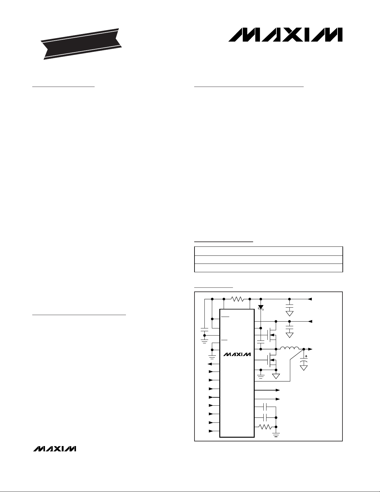
MAX8720
Dynamically Adjustable 6-Bit VID
Step-Down Controller
________________________________________________________________ Maxim Integrated Products 1
Ordering Information
MAX8720
PGOOD
VID0
VID1
VID2
VID3
VID4
VID5
SUS
AGND
OUTPUT (V
OUT
)
0.275V TO 1.850V
INPUT (V
IN
)
7V TO 28V
BST
V+
DH
LX
DL
PGND
FB
V
CC
V
DD
SHDN
+5V BIAS
FBS
GNDS
CC
REF
TIME
SKIP
D0
D1
D2
D3
D4
D5
S0
S1
ILIM
Minimal Operating Circuit
19-3319; Rev 1; 8/04
For pricing, delivery, and ordering information, please contact Maxim/Dallas Direct! at
1-888-629-4642, or visit Maxim’s website at www.maxim-ic.com.
EVALUATION KIT
AVAILABLE
PART
PIN-PACKAGE
MAX8720EEI
28 QSOP
MAX8720ETX
36 Thin QFN 6mm x 6mm
Quick-PWM is a trademark of Maxim Integrated Products, Inc.
Pin Configurations appear at end of data sheet.
TEMP RANGE
-40°C to +85°C
-40°C to +85°C
Page 2
MAX8720
Dynamically Adjustable 6-Bit VID
Step-Down Controller
2 _______________________________________________________________________________________
ABSOLUTE MAXIMUM RATINGS (Note 1)
Stresses beyond those listed under “Absolute Maximum Ratings” may cause permanent damage to the device. These are stress ratings only, and functional
operation of the device at these or any other conditions beyond those indicated in the operational sections of the specifications is not implied. Exposure to
absolute maximum rating conditions for extended periods may affect device reliability.
VCCto AGND............................................................-0.3V to +6V
V
DD
to PGND............................................................-0.3V to +6V
AGND to PGND .....................................................-0.3V to +0.3V
V+ to PGND............................................................-0.3V to +30V
SHDN to AGND ......................................................-0.3V to +16V
D0–D5, PGOOD, SUS, SKIP to AGND .....................-0.3V to +6V
FB, FBS, GNDS to AGND...........................-0.3V to (V
CC
+ 0.3V)
CC, ILIM, REF, TIME to AGND ...................-0.3V to (V
CC
+ 0.3V)
S0, S1, TON to AGND ................................-0.3V to (V
CC
+ 0.3V)
BST to PGND..........................................................-0.3V to +36V
LX to BST..................................................................-6V to +0.3V
DH to LX .....................................................-0.3V to (BST + 0.3V)
DL to PGND................................................-0.3V to (V
DD
+ 0.3V)
REF Short Circuit to AGND.........................................Continuous
Continuous Power Dissipation (T
A
= +70°C)
28-Pin QSOP (derate 10.8mW/°C above +70°C)........860mW
36-Pin TQFN (derate 26.3mW/°C above +70°C) .....2105mW
Operating Temperature
Extended Temperature Range .......................-40°C to +85°C
Junction Temperature......................................................+150°C
Storage Temperature Range .............................-65°C to +165°C
Lead Temperature (soldering, 10s) .................................+300°C
ELECTRICAL CHARACTERISTICS
(Circuit of Figure 1, V+ = 15V, SHDN = SKIP = VDD= VCC= +5V, V
OUT
= 1.25V, TA= 0°C to +85°C, unless otherwise noted. Typical
values are at T
A
= +25°C.)
PARAMETER
SYMBOL
CONDITIONS
MIN
TYP
MAX
UNITS
PWM CONTROLLER
Battery voltage, V+ 2 28
Input Voltage Range
V
CC
, V
DD
4.5 5.5
V
DAC codes from
0.9V to 1.85V
-1 +1 %
DAC codes from
0.45V to 0.875V
-10
DC Output Voltage Accuracy
V+ = 4.5V to 28V,
includes load
regulation error
DAC codes from
0.275V to 0.425V
-18
mV
Line Regulation Error VCC = 4.5V to 5.5V, V+ = 4.5V to 28V 5 mV
Remote-Sense Voltage Error FB to FBS or AGND to GNDS = 0 to 25mV 3 mV
FBS Input Bias Current FB, FBS
µA
GNDS Input Bias Current GNDS -1 +1 µA
FB Input Resistance
kΩ
150kHz, R
TIME
= 120kΩ -8 +8
818kHz, R
TIME
= 22kΩ -12
TIME Frequency Accuracy
38kHz, R
TIME
= 470kΩ -12
%
V+ = 5V, FB = 1.25V, TON = GND
(1000kHz)
TON = REF
(550kHz)
TON = open
(300kHz)
On-Time (Note 2) t
ON
V+ = 12V,
FB = 1.25V
TON = V
CC
(200kHz)
ns
Note 1: For the MAX8720EEI, AGND and PGND refer to a single pin designated GND.
-0.2 +0.2
115 180 265
230 260 290
165 190 215
320 355 390
465 515 565
+10
+18
+12
+12
Page 3
MAX8720
Dynamically Adjustable 6-Bit VID
Step-Down Controller
_______________________________________________________________________________________ 3
ELECTRICAL CHARACTERISTICS (continued)
(Circuit of Figure 1, V+ = 15V, SHDN = SKIP = VDD= VCC= +5V, V
OUT
= 1.25V, TA= 0°C to +85°C, unless otherwise noted. Typical
values are at T
A
= +25°C.)
PARAMETER
CONDITIONS
UNITS
TON = VCC, open, or REF (200kHz, 300kHz,
or 550kHz)
Minimum Off-Time (Note 2)
)
TON = GND (1000kHz)
ns
BIAS AND REFERENCE
Quiescent Supply Current (VCC)ICCFB forced above their regulation points
µA
Quiescent Supply Current (VDD)IDDFB forced above their regulation points <1 5 µA
Quiescent Battery Supply
Current (V+)
I
+
25 40 µA
Shutdown Supply Current (VCC)ICCSHDN = GND 10 25 µA
Shutdown Supply Current (VDD)IDDSHDN = GND <1 5 µA
Shutdown Battery Supply
Current (V+)
I
+
SHDN = GND, VCC = VDD = 0V or 5V <1 5 µA
Reference Voltage V
REF
VCC = 4.5V to 5.5V,
I
REF
= 0
T
A
= 0°C to +85°C
V
Reference Load Regulation ∆V
REFIREF
= 0 to 50µA
V
REF Sink Current REF in regulation 10 µA
FAULT DETECTION
VCC Undervoltage-Lockout
Threshold
Rising edge, hysteresis = 20mV, PWM
disabled below this level
4.1 4.4 V
Output Overvoltage Trip
Threshold
V
Output Overvoltage FaultPropagation Delay
t
OVP
FB forced 2% above regulation 10 µs
Output Undervoltage-Protection
Trip Threshold
With respect to unloaded output voltage 65 70 75 %
Output Undervoltage FaultPropagation Delay
t
UVP
FB forced 2% below trip threshold 10 µs
PGOOD Transition Blanking Time
After X = Y, clock speed set by R
TIME
8 clk
PGOOD Lower Trip Threshold
Measured at FB with respect to unloaded
output voltage, hysteresis = 1%
-17 -15 -13 %
PGOOD Upper Trip Threshold
Measured at FB with respect to unloaded
output voltage, hysteresis = 1%
%
PGOOD Propagation Delay
Falling edge, 50mV overdrive 10 µs
PGOOD Output Low Voltage I
SINK
= 4mA 0.4 V
PGOOD Leakage Current
High state, PGOOD forced to 5.5V 1 µA
Thermal-Shutdown Threshold T
SHDN
Hysteresis = 10°C
°C
CURRENT LIMIT
ILIM Adjustment Range 0.5
V
SYMBOL
t
OFF(MIN
t
PGOOD
I
PGOOD
MIN TYP MAX
400 500
300 375
700 1200
TA = + 25°C to + 85°C 1.985 2.00 2.015
1.98 2.00 2.02
2.20 2.25 2.30
+13 +15 +17
+150
0.01
V
REF
Page 4
MAX8720
Dynamically Adjustable 6-Bit VID
Step-Down Controller
4 _______________________________________________________________________________________
ELECTRICAL CHARACTERISTICS (continued)
(Circuit of Figure 1, V+ = 15V, SHDN = SKIP = VDD= VCC= +5V, V
OUT
= 1.25V, TA= 0°C to +85°C, unless otherwise noted. Typical
values are at T
A
= +25°C.)
PARAMETER
CONDITIONS
UNITS
90
Current-Limit Threshold (Fixed) V
LIMIT
V
PGND
- V
LX
,
ILIM = V
CC T
A
= 0°C to +85°C85
mV
V
ILIM
= 2.00V
Current-Limit Threshold
(Adjustable)
V
LIMIT
V
PGND
- V
LX
V
ILIM
= 0.50V 35 50 65
mV
VLX - V
PGND
, SKIP = ILIM = VCC,
-90 mV
Current-Limit Threshold
(Negative)
V
NEG
V
LX
- V
PGND
, SKIP = VCC, adjustable mode,
percent of current limit
%
Current-Limit Threshold (Zero
Crossing)
V
ZX
V
PGND
- V
LX
, SKIP = GND 4 mV
Current-Limit Default
Switchover Threshold
3
1
V
CC
-
0.4
V
ILIM Leakage Current 0.1 µA
GATE DRIVERS
QSOP package 1.0 3.5
DH Gate-Driver On-Resistance
(Note 3)
R
DH
TQFN package 1.0 4.5
Ω
QSOP package 1.0 3.5
DL, high state
TQFN package 1.0 4.0
DL Gate-Driver On-Resistance
(Note 3)
R
DL
DL, low state 0.4 1.0
Ω
DH Gate-Driver Source/Sink
Current
I
DH
DH forced to 2.5V, BST-LX forced to 5V 2 A
DL Gate-Driver Source Current
I
DL
(
)
DL forced to 2.5V 1.6 A
DL Gate-Driver Sink Current
)
DL forced to 2.5V 4 A
DL rising 35
Dead Time t
DEAD
DH rising 26
ns
INPUTS AND OUTPUTS
Logic high 2.4
Logic low 0.4
SHDN Input Level V
SHDN
No-fault mode 12 15
V
Logic Input High Voltage V
IH
D0–D5, SKIP, SUS 2.4 V
Logic Input Low Voltage V
IL
D0–D5, SKIP, SUS 0.8 V
Logic Input Current D0–D5, SKIP, SUS -1 +1 µA
High
V
CC
-
0.2
Open
REF
Four-Level Input Logic TON, S0, S1
GND 0.5
V
Input Leakage Current SHDN, TON, S0, S1 forced to VCC or GND -3 +3 µA
SYMBOL
TA = +25°C to +85°C
MIN TYP MAX
100 110
115
165 200 230
-140 -117
-117
BST-LX forced to 5V
VCC -
SOURCE
I
DL (SINK
3.15 3.85
1.65 2.35
Page 5

MAX8720
Dynamically Adjustable 6-Bit VID
Step-Down Controller
_______________________________________________________________________________________ 5
ELECTRICAL CHARACTERISTICS
(Circuit of Figure 1, V+ =15V, SHDN = SKIP = V
DD
= VCC= +5V, V
OUT
= 1.25V, TA= -40°C to +85°C, unless otherwise noted.
Typical values are at T
A
= +25°C.) (Note 4)
PARAMETER
CONDITIONS
UNITS
PWM CONTROLLER
Battery Voltage, V+ 2 28
Input Voltage Range
V
CC
, V
DD
4.5 5.5
V
DAC codes from 0.9V
to 1.85V
-1 +1 %
DAC codes from
0.45V to 0.875V
-15
DC Output Voltage Accuracy
V+ = 4.5V to 28V,
includes load
regulation error
DAC codes from
0.275V to 0.425V
-18
mV
FB Input Resistance
265 kΩ
150kHz, R
TIME
= 120kΩ -8 +8
818kHz, R
TIME
= 22kΩ -12
TIME Frequency Accuracy
38kHz, R
TIME
= 470kΩ -12
%
V+ = 5V, FB = 1.25V, TON = GND
(1000kHz)
290
TON = REF
(550kHz)
215
TON = open
(300kHz)
390
On-Time (Note 2) t
ON
V+ = 12V,
FB = 1.25V
TON = V
CC
(200kHz)
565
ns
TON = VCC, open, or REF (200kHz, 300kHz,
or 550kHz)
500
Minimum Off-Time (Note 2)
)
TON = GND (1000kHz) 375
ns
BIAS AND REFERENCE
Quiescent Supply Current (VCC)ICCFB forced above their regulation points
µA
Quiescent Supply Current (VDD)IDDFB forced above their regulation points 5 µA
Quiescent Battery Supply
Current (V+)
I
+
40 µA
Shutdown Supply Current (VCC)ICCSHDN = GND 25 µA
Shutdown Supply Current (VDD)IDDSHDN = GND 5 µA
Shutdown Battery Supply
Current (V+)
I
+
SHDN = GND, VCC = VDD = 0V or 5V 5 µA
Reference Voltage V
REF
VCC = 4.5V to 5.5V, no REF load
V
FAULT DETECTION
VCC Undervoltage-Lockout
Threshold
Rising edge, hysteresis = 20mV, PWM
disabled below this level
4.1 4.4 V
SYMBOL
t
OFF(MIN
MIN TYP MAX
115
230
165
320
465
1.98 2.02
+15
+18
+12
+12
1300
Page 6
MAX8720
Dynamically Adjustable 6-Bit VID
Step-Down Controller
6 _______________________________________________________________________________________
ELECTRICAL CHARACTERISTICS (continued)
(Circuit of Figure 1, V+ =15V, SHDN = SKIP = V
DD
= VCC= +5V, V
OUT
= 1.25V, TA= -40°C to +85°C, unless otherwise noted.
Typical values are at T
A
= +25°C.) (Note 4)
PARAMETER
SYMBOL
CONDITIONS
MIN
TYP
MAX
UNITS
Output Overvoltage Trip
Threshold
V
Output Undervoltage-Protection
Trip Threshold
With respect to unloaded output voltage 65 75 %
PGOOD Lower Trip Threshold
Measured at FB with respect to unloaded
output voltage, hysteresis = 1%
%
PGOOD Upper Trip Threshold
Measured at FB with respect to unloaded
output voltage, hysteresis = 1%
%
CURRENT LIMIT
ILIM Adjustment Range 0.5
V
Current-Limit Threshold (Fixed) V
LIMIT
V
PGND
- VLX, ILIM = V
CC
80 115 mV
V
ILIM
= 2.00V
240
Current-Limit Threshold
(Adjustable)
V
LIMIT
V
PGND
- V
LX
V
ILIM
= 0.50V 33 65
mV
Current-Limit Threshold
(Negative)
V
NEG
VLX - V
PGND
, SKIP = ILIM = V
CC
-85 mV
GATE DRIVERS
QSOP package 3.5
DH Gate-Driver On-Resistance
(Note 3)
R
DH
TQFN package 4.5
Ω
QSOP package 3.5
DL, high state
TQFN package 4.0
DL Gate-Driver On-Resistance
(Note 3)
R
DL
DL, low state 1.0
Ω
INPUTS AND OUTPUTS
Logic high 2.4
Logic low 0.4SHDN Input Level V
SHDN
No-fault mode 12 15
V
Logic Input High Voltage V
IH
D0–D5, SKIP, SUS 2.4 V
Logic Input Low Voltage V
IL
D0–D5, SKIP, SUS 0.8 V
High
V
CC
-
0.2
Open
REF
Four-Level Input Logic TON, S0, S1
GND 0.5
V
Note 2: On-time specifications are measured from 50% to 50% at the DH pin, with LX forced to 0, BST forced to 5V, and a 500pF
capacitor from DH to LX to simulate external MOSFET gate capacitance. Actual in-circuit times may be different due to
MOSFET switching speeds.
Note 3: Production testing limitations due to package handling require relaxed maximum on-resistance specifications for the thin
QFN package. The QSOP and thin QFN package contain the same die, and the thin QFN package imposes no additional
resistance in the circuit.
Note 4: Specifications to -40°C are guaranteed by design, not production tested.
2.20 2.30
BST-LX forced to 5V
-17.5 -12.5
+12.5 +17.5
V
REF
160
-140
3.15 3.85
1.65 2.35
Page 7
MAX8720
Dynamically Adjustable 6-Bit VID
Step-Down Controller
_______________________________________________________________________________________ 7
EFFICIENCY vs. LOAD CURRENT
(V
OUT
= 1.25V)
MAX8720 toc01
LOAD CURRENT (A)
EFFICIENCY (%)
1010.1
60
70
80
90
100
50
0.01 100
VIN = 12V
VIN = 20V
VIN = 7V
SKIP = GND
SKIP = V
CC
OUTPUT VOLTAGE vs. LOAD CURRENT
(V
OUT
= 1.25V)
MAX8720 toc02
LOAD CURRENT (A)
OUTPUT VOLTAGE (V)
15105
1.250
1.255
1.245
020
SKIP MODE
PWM MODE
SWITCHING FREQUENCY
vs. INPUT VOLTAGE
MAX8720 toc04
INPUT VOLTAGE (V)
FREQUENCY (kHz)
201510
290
300
310
320
330
340
350
360
280
525
I
OUT
= 18A
I
OUT
= 3A
SKIP = V
CC
NO-LOAD SUPPLY CURRENT
vs. INPUT VOLTAGE (PWM MODE)
MAX8720 toc05
INPUT VOLTAGE (V)
SUPPLY CURRENT (mA)
201510
5
10
15
20
25
30
0
525
ICC + I
DD
IIN
NO-LOAD SUPPLY CURRENT
vs. INPUT VOLTAGE (SKIP MODE)
MAX8720 toc06
INPUT VOLTAGE (V)
SUPPLY CURRENT (mA)
201510
0.1
0.2
0.3
0.4
0.5
0.6
0.7
0.8
0.9
1.0
0
525
I
IN
ICC + I
DD
1.990
1.994
2.002
1.998
2.006
2.010
-20 200406080100
REFERENCE LOAD REGULATION
MAX8720 toc07
I
REF
(µA)
REFERENCE VOLTAGE (V)
Typical Operating Characteristics
(MAX8720 Circuit of Figure 1, VIN= 12V, VDD= VCC= 5V, TON = open, TA= +25°C, unless otherwise noted.)
SWITCHING FREQUENCY
vs. LOAD CURRENT
MAX8720 toc03
LOAD CURRENT (A)
SWITCHING FREQUENCY (kHz)
15105
100
200
300
400
0
020
PWM MODE
SKIP MODE
Page 8

MAX8720
Dynamically Adjustable 6-Bit VID
Step-Down Controller
8 _______________________________________________________________________________________
Typical Operating Characteristics (continued)
(MAX8720 Circuit of Figure 1, VIN= 12V, VDD= VCC= 5V, TON = open, TA= +25°C, unless otherwise noted.)
2ms/div
V
CC
UVLO WAVEFORM
1.25V
MAX8720 toc10
0
0
0
5V
4V
A
B
C
D
I
OUT
= 1A
A = V
OUT
, 500mV/div
B = V
CC
, 2V/div
C = DL, 5V/div
D = PGOOD, 5V/div
20µs/div
LOAD TRANSIENT
(SKIP MODE)
1.25V
MAX8720 toc11
0
10A
0
0
12V
A
B
C
D
SKIP = GND, I
OUT
= 1A TO 11A TO 1A
A = V
OUT
, 50mV/div
B = LX, 10V/div
C = CONTROL, 5V/div
D = INDUCTOR CURRENT, 10A/div
20µs/div
LOAD TRANSIENT
(PWM MODE)
1.25V
MAX8720 toc12
0
10A
0
0
12V
A
B
C
D
SKIP = VCC, I
OUT
= 1A TO 11A TO 1A
A = V
OUT
, 50mV/div
B = LX, 10V/div
C = CONTROL, 5V/div
D = INDUCTOR CURRENT, 10A/div
50µs/div
DYNAMIC OUTPUT VOLTAGE TRANSITION
(SKIP MODE)
1.65V
MAX8720 toc13
0
10A
0
0
1.25V
12V
A
B
C
D
SKIP = GND, I
OUT
= 0.2A
A = V
OUT
, 200mV/div
B = LX, 10V/div
C = D4, 5V/div
D = INDUCTOR CURRENT, 10A/div
-10A
500µs/div
STARTUP WAVEFORMS (NO LOAD)
1.25V
MAX8720 toc08
0
0
0
0
5V
5A
-5A
A
B
C
D
I
OUT
= NO LOAD
A = V
OUT
, 500mV/div
B = PGOOD, 5V/div
C = SHDN, 5V/div
D = INDUCTOR CURRENT, 5A/div
500µs/div
STARTUP WAVEFORMS (HEAVY LOAD)
1.25V
MAX8720 toc09
0
0
0
0
5V
10A
A
B
C
D
I
OUT
= 10A
A = V
OUT
, 500mV/div
B = PGOOD, 5V/div
C = SHDN, 5V/div
D = INDUCTOR CURRENT, 10A/div
Page 9

0
5
15
10
20
25
1.995
REFERENCE VOLTAGE DISTRIBUTION
MAX8720 toc18
REFERENCE VOLTAGE (V)
SAMPLE PERCENTAGE (%)
1.998 2.0052.0022.000
100
µs/div
SUSPEND TRANSITION
(SKIP MODE)
1.25V
MAX8720 toc15
0
10A
0
0
12V
A
B
C
D
SKIP = GND, I
OUT
= 0.2A
A = V
OUT
, 500mV/div
B = LX, 10V/div
C = D4, 5V/div
D = INDUCTOR CURRENT, 10A/div
-10A
0.65V
5V
0
5
15
10
20
25
-0.48
OUTPUT VOLTAGE DISTRIBUTION
MAX8720 toc17
OUTPUT VOLTAGE ERROR (%)
SAMPLE PERCENTAGE (%)
-0.24 0.480.240.00
V
OUT
= 1.25V
50µs/div
DYNAMIC OUTPUT VOLTAGE TRANSITION
(PWM MODE)
1.65V
MAX8720 toc14
0
10A
0
0
1.25V
12V
A
B
C
D
SKIP = VCC, I
OUT
= 0.2A
A = V
OUT
, 200mV/div
B = LX, 10V/div
C = D4, 5V/div
D = INDUCTOR CURRENT, 10A/div
-10A
100µs/div
SUSPEND TRANSITION
(PWM MODE)
1.25V
MAX8720 toc16
0
10A
0
0
12V
A
B
C
D
SKIP = VCC, I
OUT
= 0.2A
A = V
OUT
, 500mV/div
B = LX, 10V/div
C = D4, 5V/div
D = INDUCTOR CURRENT, 10A/div
-10A
0.65V
5V
MAX8720
Dynamically Adjustable 6-Bit VID
Step-Down Controller
_______________________________________________________________________________________ 9
Typical Operating Characteristics (continued)
(MAX8720 Circuit of Figure 1, VIN= 12V, VDD= VCC= 5V, TON = open, TA= +25°C, unless otherwise noted.)
Page 10
MAX8720
Dynamically Adjustable 6-Bit VID
Step-Down Controller
10 ______________________________________________________________________________________
Pin Description
PIN
28 QSOP
36 THIN
QFN
NAME FUNCTION
133V+
Battery Voltage-Sense Connection. Connect V+ to input power source. V+ is used only
for PWM one-shot timing. DH on-time is inversely proportional to input voltage over a 2V
to 28V range.
234SHDN
Shutdown Control Input. Connect SHDN to V
CC
for normal operation. Connect SHDN to
GND to put the controller into its shutdown state. Forcing SHDN to 12V to 15V disables
both the overvoltage-protection and undervoltage-protection circuits and clears the fault
latch. Do not connect SHDN to >15V.
335TIME
Slew-Rate Adjustment Pin. Connect a resistor from TIME to GND to set the internal slewrate clock. A 470kΩ to 22kΩ resistor sets the clock from 38kHz to 818kHz, f
SLEW
=
150kHz x 120kΩ / R
TIME
. To reduce inrush current, f
SLEW
= 150kHz x 120kΩ / 4 x R
TIME
during power-up and power-down transient.
41FB
Fast Feedback Input. Connect FB to the junction of the external inductor and outputcapacitor node (Figure 1).
52FBS
Feed b ack Rem ote- S ense Inp ut. For nonvol tag e- p osi ti oned ci r cui ts, connect FBS to V
OU T
d i r ectl y at the l oad . FBS i nter nal l y connects to the i nteg r ator that fi ne tunes the D C outp ut
vol tag e. For vol tag e- p osi ti oned ci r cui ts, connect FBS d i r ectl y to FB near the IC to d i sab l e the
FBS r em ote- sense i nteg r ator am p l i fi er . To d i sab l e al l thr ee i nteg r ator am p l i fi er s, connect FBS
to V
C C
.
63CC
Integ r ator C ap aci tor C onnecti on. C onnect a 47p F to 1000p F ( 47p F typ ) cap aci tor fr om C C to
AGN D to set the i nteg r ati on ti m e constant. C C can b e l eft op en i f FBS i s connected to V
C C
.
7, 8 4, 5 S0, S1
S usp end - M od e V ol tag e- S el ect Inp ut. S 0 and S 1 ar e four - l evel d i g i tal i np uts that sel ect the
susp end - m od e V ID cod e for the susp end - m od e m ul ti p l exer i np uts. If S U S i s h i g h, the
susp end - m od e V ID cod e i s d el i ver ed to the D AC .
97V
CC
Anal og S up p l y Inp ut. C onnect to the system sup p l y vol tag e ( + 4.5V to + 5.5V ) thr oug h a ser i es
10Ω r esi stor . Byp ass V
C C
to anal og g r ound w i th a 1µF or g r eater cer am i c cap aci tor .
10 8 TON
On-Time Selection Control Input. This is a four-level input that sets the K-factor to
determine DH on-time. Connect TON to the following pins for the indicated operation:
GND = 1000kHz
REF = 550kHz
Open = 300kHz
V
CC
= 200kHz
11 9 REF
2.0V Reference Voltage Output. Bypass REF to analog ground with a 0.22µF or greater
ceramic capacitor. The reference can source up to 50µA for external loads. Loading REF
degrades output voltage accuracy according to the REF load regulation error.
12 10 ILIM
Current-Limit Adjustment. The PGND–LX current-limit threshold defaults to 100mV if ILIM
is connected to V
CC
. In adjustable mode, the current-limit threshold voltage is 1/10th the
voltage seen at ILIM over a 0.5V to 3.0V range. The logic threshold for switchover to the
100mV default value is approximately V
CC
- 1V. Connect ILIM to REF for a fixed 200mV
threshold.
Page 11

MAX8720
Dynamically Adjustable 6-Bit VID
Step-Down Controller
______________________________________________________________________________________ 11
Pin Description (continued)
PIN
28 QSOP
36 THIN
QFN
NAME FUNCTION
13 11 GNDS
Ground Remote-Sense Input. For nonvoltage-positioned circuits, connect GNDS to
ground directly at the load. GNDS internally connects to the integrator that fine tunes the
output voltage. The output voltage rises by an amount of GNDS - AGND. For voltagepositioned circuits, increase the output voltage by biasing GNDS with a resistor-divider
from REF to AGND.
14 12
Open-Drain Power-Good Output. PGOOD is normally high when the output is in
regulation. If V
FB
is not within a ±15% window of the DAC setting, PGOOD is asserted
low. During DAC code transitions, PGOOD is forced high for an additional 8 clocks after
the slew-rate controller finishes the transition. PGOOD is low during shutdown. PGOOD
upper threshold is blanked whenever the MAX8720 is in pulse-skipping mode (SKIP =
GND or SUS = high).
15 — GND Analog and Power Ground. Also connects to the current-limit comparator.
16 16, 17 DL Low-Side Gate-Driver Output. DL swings from PGND to VDD.
17 19 V
DD
Supply Voltage Input for the DL Gate Driver. Connect to the system supply voltage
(+4.5V to +5.5V). Bypass VDD to power ground with a 1µF or greater ceramic capacitor.
18 20 SUS
S usp end - M od e C ontr ol Inp ut. When S U S i s hi g h, the susp end - m od e V ID cod e, as
p r og r am m ed b y S 0 and S 1, i s d el i ve r ed to the D AC . C onnect S U S to G N D i f the susp end m od e m ul ti p l exer i s not used . P GOO D up p er thr eshol d i s b l anked w hen S U S i s hi g h.
19 21 D0 DAC Code Inputs. D0 is the LSB and D5 is the MSB for the 6-bit DAC.
20 22 SKIP
Pulse-Skipping Control Input. Connect SKIP to V
CC
for low-noise, forced-PWM mode, or
connect SKIP to GND to enable pulse-skipping operation. PGOOD upper threshold is
blanked when SKIP = GND.
21 23 D5
22 24 D4
23 25 D3
24 26 D2
25 27 D1
DAC Code Inputs. D0 is the LSB and D5 is the MSB for the 6-bit DAC.
26 29 BST
Boost Flying-Capacitor Connection. Connect to an external capacitor and diode as
shown in Figure 1. An optional resistor in series with BST allows the DH pullup current to
be adjusted.
27 31 LX
Inductor Connection. Connect LX to the switched side of the inductor. LX serves as the
lower supply rail for the DH high-side gate driver. It also connects to the current-limit
comparator and the skip-mode zero-crossing comparator.
28 32 DH High-Side Gate-Driver Output. DH swings from LX to BST.
—13AGND Analog Ground. Connect the backside pad to AGND.
— 14,15 PGND Power Ground. Also connects to the current-limit comparator.
—
6, 18, 28,
30, 36
N.C. Not internally connected.
PGOOD
Page 12

MAX8720
Detailed Description
The MAX8720 is a constant-on-time, quick-PWM controller with 6-bit VID inputs to dynamically set the output
voltage from 0.275V to 1.85V. The MAX8720 standard
application circuit (Figure 1) generates a low-voltage
1.25V/15A output typical of low-power CPU and GPU
core supplies in a notebook computer. The input supply range is 7V to 24V. See Table 1 for component
selections and Table 2 for component manufacturers.
5V Bias Supply (VCCand VDD)
The MAX8720 requires an external 5V bias supply in
addition to the battery. Typically, this 5V bias supply is
the notebook’s 95%-efficient, 5V system supply.
Keeping the bias supply external to the IC improves
efficiency and eliminates the cost associated with the
5V linear regulator that would otherwise be needed to
supply the PWM circuit and gate drivers. If stand-alone
capability is needed, the 5V supply can be generated
with an external linear regulator.
The 5V bias supply must provide VCC(PWM controller)
and VDD(gate-drive power), so the maximum current
drawn is:
I
BIAS
= ICC+ fSW(Q
G(LOW)
+ Q
G(HIGH)
)
= 4mA to 40mA (typ)
where ICCis 800µA (typ), fSWis the switching frequency,
and Q
G(LOW)
and Q
G(HIGH)
are the MOSFET data
sheet’s total gate-charge specification limits at VGS= 5V.
V+ and VDDcan be connected together if the input power
source is a fixed 4.5V to 5.5V supply. If the 5V bias supply
is powered up prior to the battery supply, the enable signal (SHDN going from low to high) must be delayed until
the battery voltage is present to ensure startup.
Reference (REF)
The 2V reference is accurate to ±0.75% over temperature and load, making REF useful as a precision system
reference. Bypass REF to GND with a 0.22µF or greater
ceramic capacitor. The reference sources up to 100µA
and sinks 10µA to support external loads. Loading the
reference reduces the output voltages slightly, because
of the reference load regulation error.
Dynamically Adjustable 6-Bit VID
Step-Down Controller
12 ______________________________________________________________________________________
MAX8720
PGOOD
OPEN (300kHz)
PGOOD
VID0
VID1
VID2
VID3
VID4
VID5
SUS
D
BST
V
CPU_SENSE
V
GND_SENSE
D
L
AGND*
OUTPUT
(V
OUT
)
C
OUT
(3) 470µF
L1
0.8µH
INPUT (V
IN
)
7V TO 28V
BST
C2
1µF
V+
DH
LX
DL
*PGND
FB
V
CC
V
DD
SHDN
+5V BIAS
C1
1µF
C
BST
0.1µF
C
REF
0.22µF
C
IN
(2) 10µF
FBS
CONNECT TO REMOTESENSE POINTS
*FOR THE MAX8720EEI, AGND AND PGND
REFER TO A SINGLE PIN DESIGNATED GND
GNDS
CC
REF
ILIM
SKIP
SKIP
TIME
D0
D1
D2
N
H
N
L
D3
D4
D5
S0
S1
R1
10Ω
R8
100kΩ
R2 TO R7
(6) 100kΩ
R
ILIM1
100kΩ
R
ILIM2
33.2kΩ
C
CC
47pF
+5V BIAS
TON
R
TIME
100kΩ
4-LEVEL
SUSPEND
INPUTS
OFF
PWM
ON
Figure 1. MAX8720 Standard Application Circuit
Page 13

Free-Running, Constant-On-Time PWM
Controller with Input Feed-Forward
The quick-PWM control architecture is a pseudo-fixedfrequency, constant-on-time, current-mode type with
voltage feed-forward (Figure 2). This architecture relies
on the output filter capacitor’s ESR to act as the current-sense resistor, so the output ripple voltage provides the PWM ramp signal. The control algorithm is
simple: the high-side switch on-time is determined solely by a one-shot whose period is inversely proportional
to input voltage and directly proportional to output voltage. Another one-shot sets a minimum off-time (400ns
typ). The on-time one-shot is triggered if the error comparator is low, the low-side switch current is below the
current-limit threshold, and the minimum off-time oneshot has timed out.
On-Time One-Shot (TON)
The heart of the PWM core is the one-shot that sets the
high-side switch on-time. This fast, low-jitter, adjustable
one-shot includes circuitry that varies the on-time in
response to battery and output voltage. The high-side
switch on-time is inversely proportional to the battery
voltage as measured by the V+ input, and proportional
to the output voltage. This algorithm results in a nearly
constant switching frequency despite the lack of a
fixed-frequency clock generator. The benefits of a con-
stant switching frequency are twofold: first, the frequency can be selected to avoid noise-sensitive regions
such as the 455kHz IF band; second, the inductor ripple-current operating point remains relatively constant,
resulting in easy design methodology and predictable
output voltage ripple.
On-Time = K (V
OUT
+ 0.075V) / V
IN
where K is set by the TON pin-strap connection and
0.075V is an approximation to accommodate the expected drop across the low-side MOSFET switch (Table 3).
The on-time one-shot has good accuracy at the operating points specified in the Electrical Characteristics
table (±10% at 200kHz and 300kHz, and ±12% at
550kHz and 1000kHz). On-times at operating points far
removed from the conditions specified in the Electrical
Characteristics table can vary over a wider range. For
example, the 1000kHz setting typically runs approximately 10% slower with inputs much greater than +5V
due to the very short on-times required.
MAX8720
Dynamically Adjustable 6-Bit VID
Step-Down Controller
______________________________________________________________________________________ 13
COMPONENT 15A/300kHz
Input Voltage VIN = 7V to 24V
Output Voltage V
OUT
= 1.25V
CIN Input Capacitor
(2) 10µF, 25V
TDK C3225X7R1E106M
AVX 12103D106M
Taiyo Yuden TMK325BJ106MM
C
OUT
Output Capacitor
(3) 470µF, 2.5V, 9mΩ low-ESR
polymer capacitor
Sanyo 2R5TPE470M9
NH High-Side MOSFET Siliconix SI7390DP
NL Low-Side MOSFET Siliconix SI7356DP
DL Schottky Rectifier
3A, 30V, 0.45V
f
Nihon EC31QS03L
L1 Inductor
0.8µH, 20A, 4.9mΩ
Sumida CDEP104-0R8MC-50
Table 1. Component Selection for
Standard Applications
SUPPLIER WEBSITE
AVX www.avx.com
Central Semiconductor www.centralsemi.com
Coiltronics www.coiltronics.com
Fairchild Semiconductor
www.fairchildsemi.com
Kemet www.kemet.com
Nihon www.niec.co.jp
Panasonic www.panasonic.com/industrial
Sanyo www.secc.co.jp
Siliconix (Vishay) www.vishay.com
Sumida www.sumida.com
Taiyo Yuden www.t-yuden.com
TDK www.component.tdk.com
TOKO www.tokoam.com
Table 2. Component Suppliers
TON SETTING
TON FREQUENCY
(kHz)
K-FACTOR (µs)
V
CC
200 5 ±10
Open 300 3.3 ±10
REF 550 1.8 ±12.5
GND 1000 1.0 ±12.5
Table 3. K-Factor
Page 14

MAX8720
On-times translate only roughly to switching frequencies. The on-times guaranteed in the Electrical
Characteristics table are influenced by switching delays
in the external high-side MOSFET. Resistive losses,
including the inductor, both MOSFETs, output-capacitor
ESR, and PC board copper losses in the output and
ground tend to raise the switching frequency at higher
output currents. Also, the dead-time effect increases the
effective on-time, reducing the switching frequency. It
occurs only in PWM mode (SKIP = high) and during
Dynamically Adjustable 6-Bit VID
Step-Down Controller
14 ______________________________________________________________________________________
REF
-15%
FROM
D/A
REF
REF
SKIP SUS S0, S1 D0–D5 TIME
10kΩ
ERROR
AMP
TOFF
TON
REF
+15%
FB
R-2R
D/A CONVERTER
CHIP SUPPLY
G
m
G
m
G
m
GNDS
CC
FBS
PGOOD
ON-TIME
COMPUTE
TON
ONE-SHOT
ONE-SHOT
TRIG
V
BATT
2V TO 28V
TRIG
Q
Q
S
R
2V
REF
REF
FB
PGND
+5V
V
OUT
DL
V
CC
V
DD
LX
ZERO CROSSING
CURRENT
LIMIT
DH
BST
ILIM
REF
+5V
+5V
Q
OVP/UVP
DETECT
SHDN
TON
V+
70kΩ
Σ
MAX8720
S
R
Q
MUX AND SLEW CONTROL
9
1
AGND
Figure 2. MAX8720 Block Diagram
Page 15

dynamic output-voltage transitions when the inductor
current reverses at light or negative load currents. With
reversed inductor current, the inductor’s EMF causes LX
to go high earlier than normal, extending the on-time by
a period equal to the DH-rising dead time.
For loads above the critical conduction point, where the
dead-time effect is no longer a factor, the actual switching frequency is:
where V
DIS
is the sum of the parasitic voltage drops in
the inductor discharge path, including synchronous
rectifier, inductor, and PC board resistances; V
CHG
is
the sum of the parasitic voltage drops in the inductor
charge path, including high-side switch, inductor, and
PC board resistances; and tONis the on-time calculated by the MAX8720.
Integrator Amplifiers and
Output-Voltage Offsets
Three integrator amplifiers provide a fine adjustment to
the output regulation point. One amplifier integrates the
difference between GNDS and AGND, and a second
integrates the difference between FBS and FB. The
third amplifier integrates the difference between REF
and the DAC output. These three transconductance
amplifiers’ outputs are directly summed inside the chip,
so the integration time constant can be set easily with
one capacitor. The G
m
of each amplifier is 160µS (typ).
The integrator block has the ability to lower the output
voltage by 2% and raise it by 6%. For each amplifier,
the differential input voltage range is at least ±70mV
total, including DC offset and AC ripple. The integrator
corrects for approximately 90% of the total error, due to
finite gain.
The FBS amplifier corrects for DC voltage drops in PC
board traces and connectors in the output bus path
between the DC-DC converter and the load. The GNDS
amplifier performs a similar DC correction task for the
output ground bus. The third integrator amplifier corrects the small offset of the error amplifier and provides
an averaging function that forces V
OUT
to be regulated
at the average value of the output ripple waveform.
Integrators have both beneficial and detrimental characteristics. Although they correct for drops due to DC bus
resistance and tighten the DC output-voltage tolerance
limits by averaging the peak-to-peak output ripple, they
can interfere with achieving the fastest possible loadtransient response. The fastest transient response is
achieved when all three integrators are disabled.
This can work very well if the MAX8720 circuit is placed
very close to the CPU. All three integrators can be disabled by connecting FBS to V
CC
. When the integrators
are disabled, CC can be left unconnected, which eliminates a component but leaves GNDS connected to any
convenient ground. When the inductor is in continuous
conduction, the output voltage has a DC regulation higher than the trip level by 50% of the ripple. In discontinuous conduction (SKIP = GND, light loaded), the output
voltage has a DC regulation higher than the trip level by
approximately 1.5% due to slope compensation.
There is often a connector, or at least many milliohms of
PC board trace resistance, between the DC-DC converter and the CPU. In these cases, the best strategy is
to place most of the bulk bypass capacitors close to
the CPU, with just one capacitor on the other side of the
connector near the MAX8720 to control ripple if the
CPU card is unplugged. In this situation, the remotesense lines (GNDS and FBS) and integrators provide a
real benefit.
Forced-PWM Mode (
SKIP
= High)
The low-noise forced-PWM mode (SKIP = high) disables the zero-crossing comparator, allowing the
inductor current to reverse at light loads. This causes
the low-side gate-drive waveform to become the complement of the high-side gate-drive waveform. The benefit of forced-PWM mode is to keep the switching
frequency fairly constant, but it comes at a cost: the noload battery current can be 10mA to 40mA, depending
on the external MOSFETs and switching frequency.
Forced-PWM mode is required during downward output-voltage transitions. The MAX8720 uses PWM mode
during all transitions, but only while the slew-rate controller is active. Due to voltage positioning, when a transition uses high negative inductor current, the output
voltage does not settle to its final intended value until
well after the slew-rate controller terminates. Because
of this it is possible, at very high negative slew currents,
for the output to end up high enough to cause PGOOD
to go low.
Thus, it is necessary to use forced-PWM mode during all
negative transitions. Most applications should use PWM
mode exclusively, although there is some benefit to
using skip mode while in the low-power suspend state.
Automatic Pulse-Skipping Switchover
(
SKIP
= GND)
In skip mode (SKIP = GND), an inherent automatic
switchover to PFM takes place at light loads (Figure 3).
This switchover is affected by a comparator that truncates the low-side switch on-time at the inductor current’s zero crossing. This mechanism causes the
f
VV
tVV V
SW
OUT DIS
ON IN DIS CHG
=
+
+−()
MAX8720
Dynamically Adjustable 6-Bit VID
Step-Down Controller
______________________________________________________________________________________ 15
Page 16

MAX8720
threshold between pulse-skipping PFM and nonskipping PWM operation to coincide with the boundary
between continuous and discontinuous inductor-current operation. The load-current level at which
PFM/PWM crossover occurs, I
LOAD(SKIP)
, is equal to
half the peak-to-peak ripple current, which is a function
of the inductor value (Figure 3). For a 7V to 24V battery
range, this threshold is relatively constant, with only a
minor dependence on battery voltage:
where K is the on-time scale factor (Table 2). For example, in the standard application circuit this becomes:
The crossover point occurs at a lower value if a swinging (soft-saturation) inductor is used.
The switching waveforms may appear noisy and asynchronous when light loading causes pulse-skipping
operation, but this is a normal operating condition that
results in high light-load efficiency. Trade-offs in PFM
noise vs. light-load efficiency are made by varying the
inductor value. Generally, low inductor values produce
a broader efficiency vs. load curve, while higher values
result in higher full-load efficiency (assuming that the
coil resistance remains fixed) and less output voltage
ripple. Penalties for using higher inductor values
include larger physical size and degraded load-transient response, especially at low input-voltage levels.
Current-Limit Circuit
The current-limit circuit employs a unique “valley” current-sensing algorithm that uses the on-resistance of
the low-side MOSFET as a current-sensing element. If
the current-sense signal is above the current-limit
threshold, the PWM is not allowed to initiate a new
cycle (Figure 4). The actual peak current is greater than
the current-limit threshold by an amount equal to the
inductor ripple current. Therefore, the exact currentlimit characteristic and maximum load capability are a
function of the MOSFET on-resistance, inductor value,
and battery voltage. The reward for this uncertainty is
robust, lossless overcurrent sensing. When combined
with the undervoltage-protection circuit, this currentlimit method is effective in almost every circumstance.
There is also a negative current limit that prevents
excessive reverse inductor currents when V
OUT
is
sinking current. The negative current-limit threshold
is set to approximately 120% of the positive current
limit, and therefore tracks the positive current limit
when ILIM is adjusted.
The current-limit threshold is adjusted with an external
resistor-divider at ILIM. The current-limit threshold voltage adjustment range is from 50mV to 200mV. In the
adjustable mode, the current-limit threshold voltage is
precisely 1/10th the voltage seen at ILIM. The threshold
defaults to 100mV when ILIM is connected to V
CC
. The
logic threshold for switchover to the 100mV default
value is approximately VCC- 1V.
Carefully observe the PC board layout guidelines to
ensure that noise and DC errors do not corrupt the current-sense signals seen by LX and PGND. Place the IC
close to the low-side MOSFET with short, direct traces,
making a Kelvin-sense connection to the source and
drain terminals.
MOSFET Gate Drivers (DH, DL)
The DH and DL drivers are optimized for driving moderate-sized high-side and larger low-side power MOSFETs.
This is consistent with the low duty factor seen in the
notebook CPU environment, where a large VIN- V
OUT
differential exists. An adaptive dead-time circuit monitors
the DL output and prevents the high-side FET from turning on until DL is fully off. There must be a low-resistance, low-inductance path from the DL driver to the
MOSFET gate for the adaptive dead-time circuit to work
properly. Otherwise, the sense circuitry in the MAX8720
interprets the MOSFET gate as “off” while there is actually still charge left on the gate. Use very short, wide traces
measuring 10 to 20 squares (50 to 100 mils wide if the
MOSFET is 1in from the MAX8720).
The dead time at the other edge (DH turning off) is
determined by a fixed 35ns (typ) internal delay.
The internal pulldown transistor that drives DL low is
robust, with a 0.4Ω (typ) on-resistance. This helps prevent DL from being pulled up during the fast rise time of
the inductor node, due to capacitive coupling from the
drain to the gate of the low-side synchronous-rectifier
MOSFET. Applications with high input voltages and
long, inductive DL traces may require additional gate-tosource capacitance to ensure fast-rising LX edges do
not pull up the low-side MOSFET’s gate voltage, causing shoot-through currents. The capacitive coupling
between LX and DL created by the MOSFET’s gate-todrain capacitance (C
RSS
), gate-to-source capacitance
(C
ISS
- C
RSS
), and additional board parasitics should
not exceed the minimum threshold voltage:
I
sVVV
HV
A
LOAD SKIP()
..(.)
.
.=
×−
××
=
33 125 12 125
208 12
231
µ
µ
I
KV V V
LV
LOAD SKIP
OUT IN OUT
IN
()
()
=
−
2
Dynamically Adjustable 6-Bit VID
Step-Down Controller
16 ______________________________________________________________________________________
Page 17

Lot-to-lot variation of the threshold voltage can cause
problems in marginal designs. Typically, adding
4700pF between DL and power ground (CNLin Figure
5), close to the low-side MOSFETs, greatly reduces
coupling. Do not exceed 22nF of total gate capacitance
to prevent excessive turn-off delays.
Alternatively, shoot-through currents may be caused by
a combination of fast high-side MOSFETs and slow lowside MOSFETs. If the turn-off delay time of the low-side
MOSFET is too long, the high-side MOSFETs can turn
on before the low-side MOSFETs have actually turned
off. Adding a resistor less than 5Ω in series with BST
slows down the high-side MOSFETs’ turn-on time, eliminating the shoot-through currents without degrading
the turn-off time (R
BST
in Figure 5). Slowing down the
high-side MOSFETs also reduces the LX node rise
time, thereby reducing EMI and high-frequency coupling responsible for switching noise.
VCCPOR and UVLO
Power-on reset (POR) occurs when VCCrises above
approximately 2V, resetting the fault latch and preparing the PWM for operation. VCCundervoltage-lockout
(UVLO) circuitry inhibits switching, forces PGOOD low,
and forces the DL gate driver low. When VCCrises
above 4.2V, the DAC inputs are sampled and the output voltage begins to slew to the DAC setting.
If VCCdrops low enough to trip the UVLO comparator, it
is assumed that there is not enough supply voltage to
make valid decisions. The MAX8720 immediately forces
both DH and DL low. The output discharges to 0V at a
rate dependent on the load and the total output capacitance. This prevents negative output voltages, eliminating the need for a Schottky diode to GND at the output.
For automatic startup, the battery voltage should be
present before V
CC
. If the MAX8720 attempts to bring
the output into regulation without the battery voltage
present, the fault latch trips. The SHDN pin can be toggled to reset the fault latch.
VV
C
C
GS TH IN
RSS
ISS
()
>
MAX8720
Dynamically Adjustable 6-Bit VID
Step-Down Controller
______________________________________________________________________________________ 17
INDUCTOR CURRENT
I
LOAD
= I
PEAK
/ 2
ON-TIME0TIME
I
PEAK
L
V
IN
- V
OUT
∆I
∆t
=
Figure 3. Pulse-Skipping/Discontinuous Crossover Point
INDUCTOR CURRENT
I
LIMIT
I
LOAD
0 TIME
I
PEAK
I
LIM(VAL)
= I
LOAD(MAX)
1-
LIR
2
()
Figure 4. Valley Current-Limit Threshold
MAX8720
V
DD
BST
DH
LX
(R
BST
)*
(C
NL
)*
D
BST
C
BST
C
BYP
INPUT (VIN)
N
H
L
V
DD
DL
PGND
N
L
(R
BST
)* OPTIONAL—THE RESISTOR LOWERS EMI BY DECREASING
THE SWITCHING-NODE RISE TIME.
(C
NL
)* OPTIONAL—THE CAPACITOR REDUCES LX TO DL CAPACITIVE
COUPLING THAT CAN CAUSE SHOOT-THROUGH CURRENTS.
Figure 5. Reducing the Switching-Node Rise Time
Page 18

MAX8720
Soft-Startup and Soft-Shutdown (
SHDN
)
When SHDN goes low, the MAX8720 enters low-power
shutdown mode. PGOOD goes low immediately. The
output voltage ramps down to 0V in 25mV steps at
1/4th the clock rate set by R
TIME
. The slow rampdown
of the output voltage results in smaller negative inductor currents, eliminating negative voltages on the output. When the DAC reaches the 0V setting, DL goes
high, DH goes low, the reference is turned off, and the
supply current drops to approximately 10µA.
When SHDN goes high, the reference powers up, and
after the reference UVLO is passed, the DAC target is
evaluated and switching begins. The slew-rate controller
ramps up from 0V in 25mV steps at 1/4th the clock rate
set by R
TIME
to the currently selected code value
(based on SUS). Full output current is available immediately. PGOOD goes high after the slew-rate controller
has terminated and the output voltage is in regulation.
Nominal Output Voltage Setting
The MAX8720 uses a multiplexer that selects from two
different inputs (Figure 7)—the VID DAC inputs or the
suspend-mode S0, S1 inputs. On startup, the MAX8720
slews the target voltage from ground to either the
decoded D0–D5 (SUS = low) voltage or the S0, S1 voltage (SUS = high).
DAC Inputs (D0–D5)
The digital-to-analog converter (DAC) programs the output voltage. It typically receives a preset digital code
from the CPU pins, which are either hardwired to GND
or left open-circuit. They can also be driven by digital
logic, general-purpose I/O, or an external mux. Do not
leave D0–D5 floating—use 1MΩ or less pullup resistors
if the inputs may float. D0–D5 can be changed while the
Dynamically Adjustable 6-Bit VID
Step-Down Controller
18 ______________________________________________________________________________________
PGOOD
SOFT-STARTUP AND SHUTDOWN
1/4TH SLEW RATE SET BY R
TIME
8x R
TIME
CLOCKS
V
CPU
V
CC
MODE
PGOOD
V
CPU
V
CC
PWM
DL DL
V
CC(UVLO)
FORCED-PWM MODE FORCED-PWM MODE
SHDN
SHDN
Figure 6. Soft-Startup and Soft-Shutdown
6-BIT
CODE
0
D5
D0
D1
D2
D3
D4
S1
S0
S0/S1
DECODER
OUTIN
SUS MUX
1
SEL
SUS
6-BIT
CODE
OUT
DAC
Figure 7. Internal Multiplexers Functional Diagram
Page 19

SMPS is active, initiating a transition to a new output
voltage level. If this mode of DAC control is used, connect SUS low. Change D0–D5 together, avoiding
greater than 50ns skew between bits. Otherwise, incorrect DAC readings may cause a partial transition to the
wrong voltage level, followed by the intended transition
to the correct voltage level, lengthening the overall transition time. The available DAC codes and resulting output voltages are shown in Table 4.
Suspend Mode (S0, S1, SUS)
When the CPU enters low-power suspend mode, the
processor sets the regulator to a lower output voltage
to reduce power consumption. The MAX8720 includes
a suspend-mode input (S0, S1) and a digital SUS control input. The suspend voltage is programmed using
the 4-level S0, S1 inputs (Table 5). The suspend voltage adjustment range is from 0.275V to 0.650V.
MAX8720
Dynamically Adjustable 6-Bit VID
Step-Down Controller
______________________________________________________________________________________ 19
D5 D4 D3 D2 D1 D0 V
OUT
V
OUT
0000001.850 1 0 0 0 0 0 1.050
0000011.825 1 0 0 0 0 1 1.025
0000101.800 1 0 0 0 1 0 1.000
0000111.775 1 0 0 0 1 1 0.975
0001001.750 1 0 0 1 0 0 0.950
0001011.725 1 0 0 1 0 1 0.925
0001101.700 1 0 0 1 1 0 0.900
0001111.675 1 0 0 1 1 1 0.875
0010001.650 1 0 1 0 0 0 0.850
0010011.625 1 0 1 0 0 1 0.825
0010101.600 1 0 1 0 1 0 0.800
0010111.575 1 0 1 0 1 1 0.775
0011001.550 1 0 1 1 0 0 0.750
0011011.525 1 0 1 1 0 1 0.725
0011101.500 1 0 1 1 1 0 0.700
0011111.475 1 0 1 1 1 1 0.675
0100001.450 1 1 0 0 0 0 0.650
0100011.425 1 1 0 0 0 1 0.625
0100101.400 1 1 0 0 1 0 0.600
0100111.375 1 1 0 0 1 1 0.575
0101001.350 1 1 0 1 0 0 0.550
0101011.325 1 1 0 1 0 1 0.525
0101101.300 1 1 0 1 1 0 0.500
0101111.275 1 1 0 1 1 1 0.475
0110001.250 1 1 1 0 0 0 0.450
0110011.225 1 1 1 0 0 1 0.425
0110101.200 1 1 1 0 1 0 0.400
0110111.175 1 1 1 0 1 1 0.375
0111001.150 1 1 1 1 0 0 0.350
0111011.125 1 1 1 1 0 1 0.325
0111101.100 1 1 1 1 1 0 0.300
0111111.075 1 1 1 1 1 1 0.275
Table 4. Output Voltage vs. DAC Codes
D5 D4 D3 D2 D1 D0
Page 20

MAX8720
When the CPU suspends operation (SUS = high), the
controller overrides the 6-bit VID DAC code set by
D0–D5, and slews the output voltage to the target voltage set by the S0, S1 inputs. During the transition, the
MAX8720 blanks both PGOOD thresholds (PGOOD
forced high impedance) until the slew-rate controller
reaches the suspend-mode voltage, plus 8 extra R
TIME
clocks. After this blanking time expires, the MAX8720
automatically switches to a pulse-skipping control
scheme regardless of SKIP.
Output-Voltage-Transition Timing
The MAX8720 is designed to perform output-voltage
transitions in a controlled manner, automatically minimizing input surge currents. This feature allows the circuit designer to achieve nearly ideal transitions,
guaranteeing just-in-time arrival at the new output-voltage level with the lowest possible peak currents for a
given output capacitance. This makes the IC ideal for
CPUs and GPUs that operate at different voltages.
At the beginning of an output-voltage transition (VID
change or SUS level change), the MAX8720 enters
forced-PWM mode and blanks the PGOOD output
(forced high impedance). PGOOD remains blanked
during the transition and is re-enabled when the slewrate controller has set the internal DAC to the final value
and 8 additional slew-rate clock periods have passed.
The slew-rate clock frequency (set by resistor R
TIME
)
must be set fast enough to ensure that the longest
required transition is completed within the allowed transition time.
The output-voltage transition is performed in 25mV
steps, preceded by a delay and followed by one addi-
tional clock period. The total time for a transition
depends on R
TIME
, the voltage difference, and the
accuracy of the MAX8720’s slew-rate clock, and is not
dependent on the total output capacitance. The greater
the output capacitance, the higher the surge current
required for the transition. The MAX8720 automatically
controls the current to the minimum level required to
complete the transition in the calculated time, as long
as the surge current is less than the current limit set by
ILIM. The transition time is given by:
where f
SLEW
= 150kHz x 120kΩ / R
TIME
, V
OLD
is the
original DAC setting, V
NEW
is the new DAC setting, and
t
DELAY
ranges from zero to a maximum of 2 / f
SLEW
.
See Time Frequency Accuracy in the Electrical Char-
acteristics table for f
SLEW
accuracy. The practical
range of R
TIME
is 22kΩ to 470kΩ, corresponding to
1.22µs to 26µs per 25mV step. Although the DAC takes
discrete 25mV steps, the output filter makes the transitions relatively smooth. The average inductor current
required to make an output-voltage transition is:
Suspend Transition
(Forced-PWM Operation Selected)
When the MAX8720 enters suspend mode while configured for forced-PWM operation (SKIP pulled high), the
controller ramps the output voltage down to the S0, S1
programmed voltage at the slew rate determined by
R
TIME
. The controller blanks PGOOD (forced high
impedance) until the transition is completed plus 8 extra
R
TIME
clocks—the internal target voltage equals the
selected S0, S1 DAC voltage. After this blanking time
expires, the controller enters pulse-skipping operation.
When exiting suspend mode (SUS pulled low), the
MAX8720 immediately enters forced-PWM mode and
ramps the output up at the slew rate set by R
TIME
. The
controller blanks PGOOD (forced high impedance) until
the transition is completed plus 8 extra R
TIME
clocks—
the internal target voltage equals the selected D0–D5
DAC voltage.
IC mVf
L AVE OUT SLEW()
=××25
t
VV
mV f
t
TRANS
OLD NEW
SLEW
DELAY
=
−
×
+
||
25
Dynamically Adjustable 6-Bit VID
Step-Down Controller
20 ______________________________________________________________________________________
S1 S0
V
OUT
S1 S0
V
OUT
GND
0.450
GND
REF
REF
0.425
GND
0.400
GND
V
CC
V
CC
0.375
REF
V
CC
0.350
REF REF
V
CC
REF
0.325
REF
V
CC
0.300
REF V
CC
V
CC
V
CC
0.275
Table 5. Suspend-Mode DAC Codes
GND 0.650 OPEN GND
0.625 OPEN
OPEN 0.600 OPEN OPEN
0.575 OPEN
GND 0.550
OPEN 0.500
0.525
0.475
GND
OPEN
Page 21

MAX8720
Dynamically Adjustable 6-Bit VID
Step-Down Controller
______________________________________________________________________________________ 21
HIGH VID VOLTAGE
LOW VID VOLTAGE
PGOOD
SUS
SKIP
HIGH IMPEDANCE HIGH IMPEDANCE
MODE FORCED-PWM FORCED-PWMPWM MODE PWM MODE
LOW VIDHIGH VID HIGH VIDD0-D5
PWM MODE
V
OUT
SLEW RATE SET BY R
TIME
8x R
TIME
CLOCKS
8x R
TIME
CLOCKS
Figure 8. VID Transition in Forced-PWM Mode (
SKIP
= High)
HIGH VID VOLTAGE
LOW VID VOLTAGE
PGOOD
SUS
SKIP
MODE FORCED-PWM FORCED-PWMSKIP MODE SKIP MODE
LOW VIDHIGH VID HIGH VIDD0-D5
SKIP MODE
HIGH IMPEDANCE HIGH IMPEDANCELOW T'HOLD ONLY LOW THRESHOLD ONLY
V
OUT
SLEW RATE SET BY R
TIME
8x R
TIME
CLOCKS
8x R
TIME
CLOCKS
LOW T'HOLD ONLY
Figure 9. VID Transition in Pulse-Skipping Mode (
SKIP
= GND)
Page 22

MAX8720
Dynamically Adjustable 6-Bit VID
Step-Down Controller
22 ______________________________________________________________________________________
D0–D5 VOLTAGE
S0, S1 VOLTAGE
PGOOD
SUS
SKIP
MODE FORCED-PWM FORCED-PWMPWM MODE PWM MODE
S0, S1D0–D5 D0–D5TARGET
AUTOSKIP MODE
HIGH IMPEDANCE HIGH IMPEDANCELOW THRESHOLD ONLY
V
OUT
SLEW RATE SET BY R
TIME
8x R
TIME
CLOCKS
8x R
TIME
CLOCKS
Figure 10. Suspend Transition in Forced-PWM Mode (
SKIP
= High)
D0–D5 VOLTAGE
S0, S1 VOLTAGE
PGOOD
SUS
SKIP
MODE FORCED-PWM FORCED-PWMSKIP MODE SKIP MODE
S0, S1D0–D5 D0–D5TARGET
AUTOSKIP MODE
HIGH IMPEDANCE HIGH IMPEDANCELOW T'HOLD ONLY LOW THRESHOLD ONLY
V
OUT
SLEW RATE SET BY R
TIME
8x R
TIME
CLOCKS
8x R
TIME
CLOCKS
LOW T'HOLD ONLY
Figure 11. Suspend Transition in Pulse-Skipping Mode (
SKIP
= GND)
Page 23

Suspend Transition (Pulse-Skipping
Operation Selected)
If the MAX8720 is configured for pulse-skipping operation (SKIP = GND) when SUS goes high, the MAX8720
immediately enters forced-PWM mode, ramping the
output voltage down to the S0, S1 programmed voltage
at the slew rate determined by R
TIME
. The controller
blanks PGOOD (forced high impedance) until the transition is completed plus 8 extra R
TIME
clocks—the
internal target voltage equals the selected S0, S1 DAC
voltage. After this blanking time expires, the controller
enters pulse-skipping operation.
When exiting suspend mode (SUS pulled low), the
MAX8720 immediately enters forced-PWM mode and
ramps the output up at the slew rate set by R
TIME
. The
controller blanks PGOOD (forced high impedance) until
the transition is completed plus 8 extra R
TIME
clocks—
the internal target voltage equals the selected D0–D5
DAC voltage. After this blanking time expires, the controller returns to pulse-skipping operation.
Output Overvoltage Protection
The overvoltage-protection (OVP) circuit is designed to
protect the CPU against a shorted high-side MOSFET
by drawing high current and blowing the battery fuse.
The output voltage is continuously monitored for overvoltage. If the output is more than 2.25V, OVP is triggered and the circuit shuts down. The DL low-side
gate-driver output is then latched high until SHDN is
toggled or VCCpower is cycled below 1V. This action
turns on the synchronous-rectifier MOSFET with 100%
duty and, in turn, rapidly discharges the output filter
capacitor and forces the output to ground. If the condition that caused the overvoltage (such as a shorted
high-side MOSFET) persists, the battery fuse blows. DL
is also kept high continuously in shutdown when V
CC
is
above the UVLO threshold.
Output Undervoltage Shutdown
The output UVP function is similar to foldback current
limiting, but employs a timer rather than a variable current limit. If the MAX8720 output voltage is under 70%
of the nominal value, the PWM is latched off and won’t
restart until VCCpower is cycled or SHDN is toggled.
To allow startup, UVP is ignored until the internal DAC
reaches the final target plus 8 extra R
TIME
clocks.
UVP can be defeated through the no-fault test mode
(see the No-Fault Test Mode section).
No-Fault Test Mode
The over/undervoltage-protection features can complicate the process of debugging prototype breadboards
since there are (at most) a few milliseconds in which to
determine what went wrong. Therefore, a test mode is
provided to disable the OVP, UVP, and thermal-shutdown features, and clear the fault latch if it has been
set. The no-fault test mode is entered by forcing 12V to
15V on SHDN.
Design Procedure
Firmly establish the input voltage range and maximum
load current before choosing a switching frequency
and inductor operating point (ripple-current ratio). The
primary design trade-off lies in choosing a good switching frequency and inductor operating point, and the following four factors dictate the rest of the design:
• Input Voltage Range. The maximum value
(V
IN(MAX)
) must accommodate the worst-case, high
AC-adapter voltage. The minimum value (V
IN(MIN)
)
must account for the lowest battery voltage after
drops due to connectors, fuses, and battery selector
switches. If there is a choice at all, lower input voltages result in better efficiency.
• Maximum Load Current. There are two values to
consider. The peak load current (I
LOAD(MAX)
) determines the instantaneous component stresses and filtering requirements and thus drives output-capacitor
selection, inductor saturation rating, and the design of
the current-limit circuit. The continuous load current
(I
LOAD
) determines the thermal stresses and thus drives the selection of input capacitors, MOSFETs, and
other critical heat-contributing components.
• Switching Frequency. This choice determines the
basic trade-off between size and efficiency. The
optimal frequency is largely a function of maximum
input voltage, due to MOSFET switching losses that
are proportional to frequency and V
IN
2
. The optimum frequency is also a moving target, due to rapid
improvements in MOSFET technology that are making higher frequencies more practical.
• Inductor Operating Point. This choice provides
trade-offs between size vs. efficiency, and transient
response vs. output ripple. Low inductor values provide better transient response and smaller physical
size, but also result in lower efficiency and higher
output ripple due to increased ripple currents. The
minimum practical inductor value is one that causes
the circuit to operate at the edge of critical conduction (where the inductor current just touches zero
with every cycle at maximum load). Inductor values
lower than this grant no further size-reduction benefit.
The optimum operating point is usually found
between 20% and 50% ripple current. When pulse
skipping (SKIP low and light loads), the inductor
MAX8720
Dynamically Adjustable 6-Bit VID
Step-Down Controller
______________________________________________________________________________________ 23
Page 24

MAX8720
value also determines the load-current value at
which PFM/PWM switchover occurs.
Inductor Selection
The switching frequency and inductor operating point
determine the inductor value as follows:
For example: I
LOAD(MAX)
= 15A, VIN= 12V, V
OUT
=
1.25V, fSW= 300kHz, 30% ripple current or LIR = 0.3
Find a low-loss inductor with the lowest possible DC
resistance that fits in the allotted dimensions. Ferrite
cores are often the best choice, although powdered
iron is inexpensive and can work well at 200kHz. The
core must be large enough not to saturate at the peak
inductor current (I
PEAK
):
Most inductor manufacturers provide inductors in standard values, such as 1.0µH, 1.5µH, 2.2µH, 3.3µH, etc.
Also look for nonstandard values, which can provide a
better compromise in LIR across the input voltage
range. If using a swinging inductor (where the no-load
inductance decreases linearly with increasing current),
evaluate the LIR with properly scaled inductance values.
Transient Response
The inductor ripple current also impacts transientresponse performance, especially at low VIN- V
OUT
differentials. Low inductor values allow the inductor
current to slew faster, replenishing charge removed
from the output filter capacitors by a sudden load step.
The total output-voltage sag is the sum of the voltage
sag while the inductor is ramping up and the voltage
sag before the next pulse can occur.
where t
OFF(MIN)
is the minimum off-time (see the
Electrical Characteristics) and K is from Table 3.
The amount of overshoot during a full-load to no-load
transient due to stored inductor energy can be calculated as:
Setting the Current Limit
The minimum current-limit threshold must be great
enough to support the maximum load current when the
current limit is at the minimum tolerance value. The
peak inductor current occurs at I
LOAD(MAX)
plus half
the ripple current; therefore:
where I
LIMIT(LOW)
equals the minimum current-limit
threshold voltage divided by the R
DS(ON)
of NL. For the
100mV default setting, the minimum current-limit
threshold is 90mV.
Connect ILIM to VCCfor a default 100mV current-limit
threshold. For an adjustable threshold, connect a resistor-divider from REF to GND, with ILIM connected to the
center tap. The external adjustment range of 0.5V to 2.0V
corresponds to a current-limit threshold of 50mV to
200mV. When adjusting the current limit, use 1% tolerance resistors and a 10µA divider current to prevent a
significant increase of errors in the current-limit tolerance.
Output Capacitor Selection
The output filter capacitor must have low enough equivalent series resistance (ESR) to meet output ripple and
load-transient requirements, yet have high enough ESR
to satisfy stability requirements. The output capacitance must be high enough to absorb the inductor
energy while transitioning from full-load to no-load conditions without tripping the overvoltage fault protection.
When using high-capacitance, low-ESR capacitors (see
the Output-Capacitor Stability Requirements section),
the filter capacitor’s ESR dominates the output voltage
ripple. Thus, the output capacitor’s size depends on
the maximum ESR required to meet the output-voltageripple (V
RIPPLE(P-P)
) specifications:
In CPU V
CORE
converters and other applications where
the output is subject to violent load transients, the output capacitor’s size typically depends on how much
ESR is needed to prevent the output from dipping too
VRILIR
RIPPLE P P ESR ILOAD MAX() ( )−
=
II
LIR
LIMIT LOW LOAD MAX() ()
>−
1
2
V
IL
CV
SOAR
LOAD MAX
OUT OUT
≈
()
()
∆
2
2
V
LI K
V
V
t
CVK
VV
V
t
SAG
LOAD MAX
OUT
IN
OFF MIN
OUT OUT
IN OUT
IN
OFF MIN
=
+
−
−
()
() ()
()
∆
2
II
LIR
PEAK LOAD MAX
=+
()
1
2
L
VV V
V kHz A
H=
×−
×××
=
125 12 125
12 300 15 0 3
083
.( .)
.
. µ
L
VVV
Vf I LIR
OUT IN OUT
IN SW LOAD MAX
=
−()
()
Dynamically Adjustable 6-Bit VID
Step-Down Controller
24 ______________________________________________________________________________________
Page 25

low under a load transient. Ignoring the sag due to
finite capacitance:
R
ESR
≤ V
STEP
/ I
LOAD(MAX)
The actual capacitance value required relates to the
physical size needed to achieve low ESR, as well as to
the chemistry of the capacitor technology. Thus, the
capacitor is usually selected by ESR and voltage rating
rather than by capacitance value (this is true of tantalums, OS-CONs, polymers, and other electrolytics).
When using low-capacity filter capacitors, such as
ceramic capacitors, size is usually determined by the
capacity needed to prevent V
SAG
and V
SOAR
from
causing problems during load transients. Generally,
once enough capacitance is added to meet the overshoot requirement, undershoot at the rising load edge
is no longer a problem (see the V
SAG
and V
SOAR
equations in the Transient Response section). However, lowcapacity filter capacitors typically have high-ESR zeros
that may affect the overall stability (see the Output-
Capacitor Stability Considerations section).
Output-Capacitor Stability Considerations
Stability is determined by the value of the ESR zero relative to the switching frequency. The boundary of instability is given by the following equation:
A voltage-positioned circuit has the ESR zero frequency lowered due to the external resistor in series with the
output-capacitor ESR, guaranteeing stability. For a voltage-positioned circuit, the minimum ESR requirement
of the output capacitor is reduced by the voltage-positioning resistor value.
The boundary condition of instability is given by the following equation:
R
ESR
x C
OUT
≥ 1 / (2 x fSW)
For good phase margin, it is recommended to increase
the equivalent RC time constant by a factor of two. The
standard application circuit (Figure 1) operating at
300kHz with C
OUT
= 1410µF and R
ESR
= 3mΩ easily
meets this requirement.
The easiest method for checking stability is to apply a
very fast zero-to-max load transient and carefully
observe the output-voltage-ripple envelope for overshoot and ringing. It can help to simultaneously monitor
the inductor current with an AC current probe. Do not
allow more than one cycle of ringing after the initial
step-response under/overshoot.
Do not put high-value ceramic capacitors directly
across the feedback sense point without taking precautions to ensure stability. Large ceramic capacitors can
have a high-ESR zero frequency and cause erratic,
unstable operation. However, it is easy to add enough
series resistance by placing the capacitors a couple of
inches downstream from the feedback sense point,
which should be as close as possible to the inductor.
Unstable operation manifests itself in two related but
distinctly different ways: double pulsing and fast-feedback loop instability. Double pulsing occurs due to
noise on the output or because the ESR is so low that
there is not enough voltage ramp in the output voltage
signal. This “fools” the error comparator into triggering
a new cycle immediately after the 400ns minimum offtime period has expired. Double pulsing is more of a
nuisance than harmful, resulting in nothing worse than
increased output ripple. However, it can indicate the
possible presence of loop instability due to insufficient
ESR. Loop instability can result in oscillations at the output after line or load steps. Such perturbations are usually damped, but can cause the output voltage to rise
above or fall below the tolerance limits.
Input Capacitor Selection
The input capacitor must meet the ripple-current
requirement (I
RMS
) imposed by the switching currents
defined by the following equation:
For most applications, nontantalum chemistries (ceramic or OS-CON) are preferred due to their resistance to
inrush surge currents typical of systems with a switch
or a connector in series with the battery. If the
MAX8720 is operated as the second stage of a twostage power-conversion system, tantalum input capacitors are acceptable. In either configuration, choose an
input capacitor that exhibits less than +10°C tempera-
ture rise at the RMS input current for optimal reliability
and lifetime.
Power MOSFET Selection
Most of the following MOSFET guidelines focus on the
challenge of obtaining high load-current capability
when using high-voltage (>20V) AC adapters. Low-current applications usually require less attention.
The high-side MOSFET (NH) must be able to dissipate
the resistive losses plus the switching losses at both
V
IN(MIN)
and V
IN(MAX)
. Ideally, the losses at V
IN(MIN)
should be roughly equal to the losses at V
IN(MAX)
, with
lower losses in between. If the losses at V
IN(MIN)
are
I
I
V
VVV
RMS
OUT MAX
IN
OUT IN OUT
=−
()
()
f
f
where f
RC
ESR
SW
ESR
ESR OUT
≤
=
π
π12
MAX8720
Dynamically Adjustable 6-Bit VID
Step-Down Controller
______________________________________________________________________________________ 25
Page 26

MAX8720
significantly higher, consider increasing the size of NH.
Conversely, if the losses at V
IN(MAX)
are significantly
higher, consider reducing the size of NH. If VINdoes
not vary over a wide range, maximum efficiency is
achieved by selecting a high-side MOSFET (NH) that
has conduction losses equal to the switching losses.
Choose a low-side MOSFET (NL) that has the lowest
possible on-resistance (R
DS(ON)
), comes in a moderate-sized package (i.e., SO-8, DPAK, or D2PAK), and is
reasonably priced. Ensure that the MAX8720 DL gate
driver can supply sufficient current to support the gate
charge and the current injected into the parasitic drainto-gate capacitor caused by the high-side MOSFET
turning on; otherwise, cross-conduction problems may
occur. Switching losses are not an issue for the lowside MOSFET since it is a zero-voltage switched device
when used in the step-down topology.
Power MOSFET Dissipation
Worst-case conduction losses occur at the duty-factor
extremes. For the high-side MOSFET (NH), the worstcase power dissipation due to resistance occurs at the
minimum input voltage:
Generally, use a small high-side MOSFET to reduce
switching losses at high input voltages. However, the
R
DS(ON)
required to stay within package power-dissipation limits often limits how small the MOSFET can be.
The optimum occurs when the switching losses equal
the conduction (R
DS(ON)
) losses. High-side switching
losses do not become an issue until the input is greater
than approximately 15V.
Calculating the power dissipation in high-side
MOSFETs (N
H
) due to switching losses is difficult, since
it must allow for difficult-to-quantify factors that influence the turn-on and turn-off times. These factors
include the internal gate resistance, gate charge,
threshold voltage, source inductance, and PC board
layout characteristics. The following switching loss calculation provides only a very rough estimate and is no
substitute for breadboard evaluation, preferably including verification using a thermocouple mounted on NH:
where C
RSS
is the reverse transfer capacitance of NH,
and I
GATE
is the peak gate-drive source/sink current
(2A typ).
Switching losses in the high-side MOSFET can become
a heat problem when maximum AC-adapter voltages
are applied, due to the squared term in the switchingloss equation (C x V
IN
2
x fSW). If the high-side MOSFET
chosen for adequate R
DS(ON)
at low battery voltages
becomes extraordinarily hot when subjected to
V
IN(MAX)
, consider choosing another MOSFET with
lower parasitic capacitance.
For the low-side MOSFET (NL), the worst-case power
dissipation always occurs at maximum battery voltage:
The absolute worst case for MOSFET power dissipation
occurs under heavy overload conditions that are
greater than I
LOAD(MAX)
but are not high enough to
exceed the current limit and cause the fault latch to trip.
To protect against this possibility, “overdesign” the circuit to tolerate:
where I
LIMIT
is the peak current allowed by the currentlimit circuit, including threshold tolerance and senseresistance variation. The MOSFETs must have a
relatively large heatsink to handle the overload power
dissipation.
Choose a Schottky diode (DL) with a forward-voltage
drop low enough to prevent the low-side MOSFET’s
body diode from turning on during the dead time. As a
general rule, select a diode with a DC current rating
equal to 1/3rd of the load current. This diode is optional
and can be removed if efficiency is not critical.
Boost Capacitors
The boost capacitors (C
BST
) must be selected large
enough to handle the gate-charging requirements of
the high-side MOSFETs. Typically, 0.1µF ceramic
capacitors work well for low-power applications driving
medium-sized MOSFETs. However, high-current applications driving large, high-side MOSFETs require boost
capacitors larger than 0.1µF. For these applications,
select the boost capacitors to avoid discharging the
capacitor more than 200mV while charging the highside MOSFETs’ gates:
C
NQ
mV
BST
GATE
=
×
200
II
I LIR
LOAD LIMIT
LOAD MAX
=−
()
2
PD N RESISTIVE
V
V
IR
L
OUT
IN MAX
LOAD DS ON
() ()
()
()
=−
1
2
PD N SWITCHING
VCfI
I
H
IN MAX RSS SW LOAD
GATE
()
()
()
=
2
PD N RESISTIVE
V
V
IR
H
OUT
IN
LOAD DS ON
()()
()
=
×
2
Dynamically Adjustable 6-Bit VID
Step-Down Controller
26 ______________________________________________________________________________________
Page 27

where N is the number of high-side MOSFETs used for
one regulator, and Q
GATE
is the gate charge specified
in the MOSFET’s data sheet. For example, assume the
IRF7821 n-channel MOSFET is used on the high side.
According to the manufacturer’s data sheet, a single
IRF7821 has a maximum gate charge of 14nC (VGS=
5V). Using the above equation, the required boost
capacitance is:
Select the closest standard value. This example
requires a 0.1µF ceramic capacitor.
Applications Information
Dropout Performance
The output-voltage adjust range for continuous-conduction operation is restricted by the nonadjustable 500ns
(max) minimum off-time one-shot (375ns max at
1000kHz). For best dropout performance, use the slower
(200kHz) on-time settings. When working with low input
voltages, the duty-factor limit must be calculated using
worst-case values for on- and off-times. Manufacturing
tolerances and internal propagation delays introduce an
error to the TON K-factor. This error is greater at higher
frequencies (Table 3). Also, keep in mind that transientresponse performance of buck regulators operated
close to dropout is poor, and bulk output capacitance
must often be added (see the V
SAG
equation in the
Design Procedure section).
The absolute point of dropout is when the inductor current ramps down during the minimum off-time (∆I
DOWN
)
as much as it ramps up during the on-time (∆IUP). The
ratio h = ∆IUP/ ∆I
DOWN
is an indicator of the ability to
slew the inductor current higher in response to
increased load, and must always be greater than 1. As
h approaches 1, the absolute minimum dropout point,
the inductor current is less able to increase during
each switching cycle and V
SAG
greatly increases
unless additional output capacitance is used.
A reasonable minimum value for h is 1.5, but this may
be adjusted up or down to allow tradeoffs between
V
SAG
, output capacitance, and minimum operating
voltage. For a given value of h, the minimum operating
voltage can be calculated as:
where V
DIS
and V
CHG
are the parasitic voltage drops in
the discharge and charge paths, respectively (see the
On-Time One-Shot (TON) section), t
OFF(MIN)
is from the
Electrical Characteristics table, and K is taken from
Table 3. The absolute minimum input voltage is calculated with h = 1.
If the calculated V
IN(MIN)
is greater than the required
minimum input voltage, then operating frequency must
be reduced or output capacitance added to obtain
an acceptable V
SAG
. If operation near dropout is
anticipated, calculate V
SAG
to be sure of adequate
transient response.
Dropout Design Example:
V
OUT
= 1.6V
fSW= 550kHz
K = 1.8µs, worst-case K = 1.58µs
t
OFF(MIN)
= 500ns
V
DIS
= V
CHG
= 100mV
h = 1.5
V
IN(MIN)
= (1.6V + 0.1V) / (1 - 0.5µs x 1.5 / 1.58µs)
+ 0.1V - 0.1V = 3.2V
Calculating again with h = 1 gives the absolute limit
of dropout:
V
IN(MIN)
= (1.6V + 0.1V) / (1 - 0.5µs x 1.0 / 1.58µs)
+ 0.1V - 0.1V = 2.5V
Therefore, V
IN
must be greater than 2.5V, even with
very large output capacitance, and a practical input
voltage with reasonable output capacitance is 3.2V.
One-Stage (Battery Input) vs. Two-Stage
(5V Input) Applications
The MAX8720 can be used with a direct battery connection (one stage) or can obtain power from a regulated 5V supply (two stage). Each approach has
advantages, and careful consideration should go into
the selection of the final design.
The one-stage approach offers smaller total inductor
size and fewer capacitors overall due to the reduced
demands on the 5V supply. The transient response of
the single stage is better due to the ability to ramp up
the inductor current faster. The total efficiency of a single stage is better than the two-stage approach.
The two-stage approach allows flexible placement due
to smaller circuit size and reduced local power dissipation. The power supply can be placed closer to the
CPU for better regulation and lower I2R losses from PC
board traces. Although the two-stage design has worse
transient response than the single stage, this can be
offset by the use of a voltage-positioned converter.
V
VV
th
K
VV
IN MIN
OUT DIS
OFF MIN
CHG DIS()
()
=
+
−
×
+−
1
C
nC
mV
F
BST
=
×=114
200
007. µ
MAX8720
Dynamically Adjustable 6-Bit VID
Step-Down Controller
______________________________________________________________________________________ 27
Page 28

MAX8720
PC Board Layout Guidelines
Careful PC board layout is critical to achieving low
switching losses and clean, stable operation. The
switching power stage requires particular attention
(Figure 12). If possible, mount all of the power components on the top side of the board, with their ground
terminals flush against one another. Follow these guidelines for good PC board layout:
• Keep the high-current paths short, especially at the
ground terminals. This practice is essential for stable, jitter-free operation.
• Keep the power traces and load connections short.
This practice is essential for high efficiency. Using
thick copper PC boards (2oz vs. 1oz) can enhance
full-load efficiency by 1% or more. Correctly routing
PC board traces is a difficult task that must be
approached in terms of fractions of centimeters,
where a single milliohm of excess trace resistance
causes a measurable efficiency penalty.
• When trade-offs in trace lengths must be made, it is
preferable to allow the inductor charging path to be
made longer than the discharge path. For example,
it is better to allow some extra distance between the
input capacitors and the high-side MOSFET than to
allow distance between the inductor and the lowside MOSFET or between the inductor and the output filter capacitor.
• Route high-speed switching nodes (BST, LX, DH, and
DL) away from sensitive analog areas (REF, FB).
Dynamically Adjustable 6-Bit VID
Step-Down Controller
28 ______________________________________________________________________________________
INDUCTOR
INPUT GROUND
OUTPUT
C
IN
C
IN
QSOP LAYOUT EXAMPLE
CONNECT AGND
AND PGND TO THE
CONTROLLER AT
ONE POINT ONLY
AS SHOWN
ANALOG
GROUND
POWER
GROUND
QFN LAYOUT EXAMPLE
CONNECT AGND
AND PGND TO THE
CONTROLLER AT
ONE POINT ONLY
AS SHOWN
ANALOG
GROUND
POWER
GROUND
V
CC
CC
REF
V
DD
C
OUT
C
OUT
C
OUT
POWER STAGE LAYOUT EXAMPLE
Figure 12. PC Board Layout Example
Page 29

Layout Procedure
1) Place the power components first, with ground terminals adjacent (NL source, CIN, C
OUT
, and DL
anode). If possible, make all these connections on
the top layer with wide, copper-filled areas.
2) Mount the controller IC adjacent to the low-side
MOSFET, preferably on the back side opposite NL
and NH to keep LX, GND, DH, and the DL gate-drive
lines short and wide. The DL and DH_ gate traces
must be short and wide (50 to 100 mils wide if the
MOSFET is 1in from the controller IC) to keep the driver impedance low and for proper adaptive deadtime sensing.
3) Group the gate-drive components (BST diode and
capacitor, VDDbypass capacitor) together near the
controller IC.
4) Make the DC-DC controller ground connections as
shown in Figures 1 and 12. This diagram can be
viewed as having two separate ground planes:
power ground, where all the high-power components go, and an analog ground plane for sensitive
analog components. The analog ground plane and
power ground plane must meet only at a single point
directly at the IC.
5) Connect the output power planes directly to the output filter capacitor positive and negative terminals
with multiple vias. Place the entire DC-DC converter
circuit as close to the load as is practical.
Chip Information
TRANSISTOR COUNT: 7190
PROCESS: BiCMOS
MAX8720
Dynamically Adjustable 6-Bit VID
Step-Down Controller
______________________________________________________________________________________ 29
28
27
26
25
24
23
22
21
20
19
18
17
16
15
1
2
3
4
5
6
7
8
9
10
11
12
13
14
DH
LX
BST
D1
D2
D3
GND
D4
D5
SKIP
D0
SUS
V
DD
DL
PGOOD
GNDS
ILIM
REF
TON
V
CC
S1
S0
CC
FBS
FB
TIME
SHDN
V+
QSOP
TOP VIEW
MAX8720EEI
D1
D2
D4
D5
SUS
V
DD
SKIP
D0
D3
CC
S0
S1
V
CC
TON
REF
FB
1
2
3
4
5
6
7
8
9
36 35 34 33 32 31 30 29 28
10 11 12 13 14 15 16 17 18
27
26
25
24
23
22
21
20
19
PGND
PGND
DL
N.C.
AGND
PGOOD
GNDS
ILIM
TIME
SHDNV+DHLXN.C.
BST
N.C.
N.C.
THIN QFN
6mm x 6mm
MAX8720ETX
N.C.
DL
FBS
Pin Configurations
Page 30

MAX8720
Dynamically Adjustable 6-Bit VID
Step-Down Controller
30 ______________________________________________________________________________________
Package Information
(The package drawing(s) in this data sheet may not reflect the most current specifications. For the latest package outline information,
go to www.maxim-ic.com/packages
.)
QSOP.EPS
E
1
1
21-0055
PACKAGE OUTLINE, QSOP .150", .025" LEAD PITCH
Page 31

MAX8720
Dynamically Adjustable 6-Bit VID
Step-Down Controller
Maxim cannot assume responsibility for use of any circuitry other than circuitry entirely embodied in a Maxim product. No circuit patent licenses are
implied. Maxim reserves the right to change the circuitry and specifications without notice at any time.
Maxim Integrated Products, 120 San Gabriel Drive, Sunnyvale, CA 94086 408-737-7600 ____________________ 31
© 2004 Maxim Integrated Products Printed USA is a registered trademark of Maxim Integrated Products.
Package Information (continued)
(The package drawing(s) in this data sheet may not reflect the most current specifications. For the latest package outline information,
go to www.maxim-ic.com/packages
.)
QFN THIN 6x6x0.8.EPS
e e
LL
A1 A2
A
E/2
E
D/2
D
E2/2
E2
(NE-1) X e
(ND-1) X e
e
D2/2
D2
b
k
k
L
C
L
C
L
C
L
C
L
E
1
2
21-0141
PACKAGE OUTLINE
36, 40, 48L THIN QFN, 6x6x0.8mm
L1
L
e
8. COPLANARITY APPLIES TO THE EXPOSED HEAT SINK SLUG AS WELL AS THE TERMINALS.
6. ND AND NE REFER TO THE NUMBER OF TERMINALS ON EACH D AND E SIDE RESPECTIVELY.
5. DIMENSION b APPLIES TO METALLIZED TERMINAL AND IS MEASURED BETWEEN 0.25 mm AND 0.30 mm
FROM TERMINAL TIP.
4. THE TERMINAL #1 IDENTIFIER AND TERMINAL NUMBERING CONVENTION SHALL CONFORM TO JESD 95-1
SPP-012. DETAILS OF TERMINAL #1 IDENTIFIER ARE OPTIONAL, BUT MUST BE LOCATED WITHIN THE
ZONE INDICATED. THE TERMINAL #1 IDENTIFIER MAY BE EITHER A MOLD OR MARKED FEATURE.
9. DRAWING CONFORMS TO JEDEC MO220, EXCEPT FOR 0.4mm LEAD PITCH PACKAGE T4866-1.
7. DEPOPULATION IS POSSIBLE IN A SYMMETRICAL FASHION.
3. N IS THE TOTAL NUMBER OF TERMINALS.
2. ALL DIMENSIONS ARE IN MILLIMETERS. ANGLES ARE IN DEGREES.
1. DIMENSIONING & TOLERANCING CONFORM TO ASME Y14.5M-1994.
NOTES:
10. WARPAGE SHALL NOT EXCEED 0.10 mm.
E
2
2
21-0141
PACKAGE OUTLINE
36, 40, 48L THIN QFN, 6x6x0.8mm
 Loading...