

Page 1
General Description
The MAX8718/MAX8719 are micropower, 8-pin TDFN
linear regulators that supply always-on, keep-alive
power to CMOS RAM, real-time clocks (RTC), and
microcontrollers in systems with high-voltage batteries.
The circuits consist of a 100mA linear regulator and a
power-good comparator (PGOOD) with fixed-output
delay. Key features include wide input voltage range,
low-dropout voltage, and low-quiescent supply current.
Despite a miserly 25µA (max) no-load quiescent current, the MAX8718/MAX8719 have good line- and loadtransient response and excellent AC power-supply
rejection. They provide a clean fixed 5V or 3.3V output
(MAX8718), or an adjustable 1.24V to 28V output
(MAX8719), even when subjected to fast supply-voltage changes that occur during the switchover from battery to AC-adapter input power. The space-saving
TDFN package has excellent thermal characteristics
and tolerates up to 1951mW of power dissipation.
Internal foldback current limiting and thermal shutdown
protect the regulator from overload and thermal faults.
In addition to the main notebook-computer application,
these devices are useful in other low-power, high-voltage applications (4V < VIN< 28V) such as smart batteries, current control loops, telecom emergency power,
and housekeeping power for off-line supplies.
The MAX8718/MAX8719 are available in a thermally
enhanced 3mm x 3mm, 8-lead TDFN package.
Applications
CMOS/RTC Backup Power
Microcontroller Power
Notebook Computers
Smart-Battery Packs
PDAs and Handy-Terminals
Battery-Powered Systems
Features
♦ 4V to 28V Input Range
♦ 18µA Quiescent Supply Current
♦ <3µA Shutdown Supply Current
♦ 100mA Output Current
♦ 3.3V or 5V, Pin-Selectable Output (MAX8718)
♦ Adjustable 1.24V to 28V Output (MAX8719)
♦ ±2% Output Accuracy
♦ Thermal-Overload Protection
♦ Delayed Power-Good Output
♦ Thermally Enhanced 8-Pin TDFN Package
MAX8718/MAX8719
High-Voltage, Low-Power Linear Regulators for
Notebook Computers
________________________________________________________________ Maxim Integrated Products 1
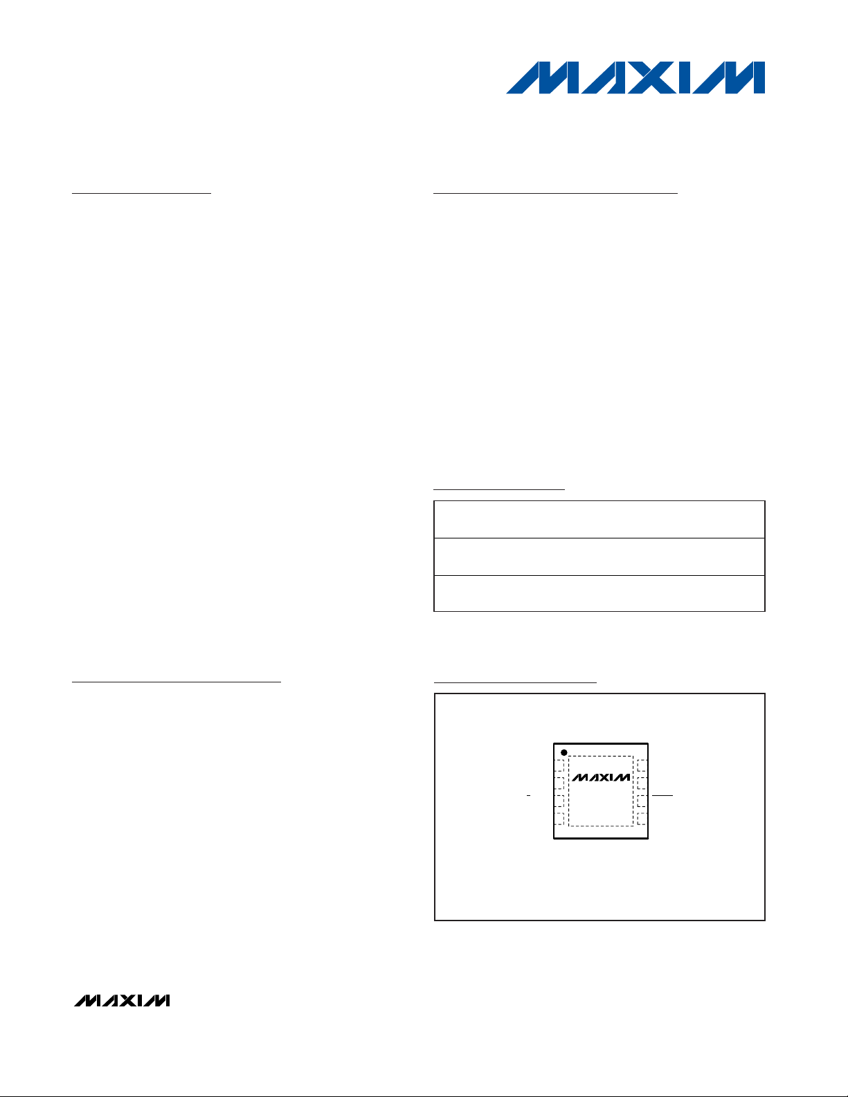
TDFN
3mm × 3mm
TOP VIEW
1
2
8
7
3
4
6
5
SHDN
PGOOD
V
CC
OUT
I.C.
GND
5/3 (FB)
IN
MAX8718
MAX8719
() ARE FOR THE MAX8719.
Pin Configuration
Ordering Information
19-3495; Rev 0; 11/04
For pricing, delivery, and ordering information, please contact Maxim/Dallas Direct! at
1-888-629-4642, or visit Maxim’s website at www.maxim-ic.com.
PART
TEMP RANGE
PIN-PACKAGE
OUTPUT
VOLTAGE
MAX8718ETA
8 TDFN 3mm x
3mm
3.3V/5V
MAX8719ETA
8 TDFN 3mm x
3mm
Adjustable
-40°C to +85°C
-40°C to +85°C
Page 2

MAX8718/MAX8719
High-Voltage, Low-Power Linear Regulators for
Notebook Computers
2 _______________________________________________________________________________________
ABSOLUTE MAXIMUM RATINGS
Stresses beyond those listed under “Absolute Maximum Ratings” may cause permanent damage to the device. These are stress ratings only, and functional
operation of the device at these or any other conditions beyond those indicated in the operational sections of the specifications is not implied. Exposure to
absolute maximum rating conditions for extended periods may affect device reliability.
IN to GND...............................................................-0.3V to +30V
SHDN to GND..............................................-0.3V to (V
IN
+ 0.3V)
5/3 (MAX8718) to GND.............................................-0.3V to +6V
FB (MAX8719) to GND.............................................-0.3V to +6V
OUT (MAX8718) to GND..........................................-0.3V to +6V
OUT (MAX8719) to GND........................................-0.3V to +30V
V
CC
to GND (MAX8718)...........................................-0.3V to +6V
V
CC
to GND (MAX8719)........................................-0.3V to +2.7V
PGOOD to GND .....................................................-0.3V to +30V
I.C. to GND...............................................................-0.3V to +6V
OUT Short Circuit to GND.......................................................30s
Continuous Power Dissipation (T
A
= +70°C)
8-Pin TDFN (derate 24.4mW/°C above +70°C) ..........1951mW
Operating Temperature Range ...........................-40°C to +85°C
Junction Temperature......................................................+150°C
Storage Temperature Range.............................-65°C to +150°C
Lead Temperature (soldering, 10s).................................+300°C
ELECTRICAL CHARACTERISTICS
(Circuit of Figure 1. VIN= 15V, I
OUT
= 5µA, TA= 0°C to +85°C. Typical values are at TA= +25°C, unless otherwise noted.) (Note 1)
PARAMETER
SYMBOL
CONDITIONS
MIN
TYP
MAX
UNITS
Input Voltage Range V
IN
428V
SHDN = IN, TA = +25°C1218µs
Supply Current (MAX8718) I
IN
SHDN = IN, VIN = 6V to 28V 25 µA
0V < VCC < 2.7V, TA = +25°C
VCC Input Current (MAX8719)
0V < V
CC
< 2.7V, TA = 0°C to +85°C
µA
0V < VCC < 5.5V, TA = +25°C 3.4
VCC Input Current (MAX8718)
0V < V
CC
< 5.5V, TA = 0°C to +85°C 2.3
µA
OUT Minimum Load Current 5µA
Shutdown Supply Current SHDN = 0V 1.2 3 µA
Dropout Supply Current V
OUT
set to 5V, VIN = 4.7V 85 µA
VIN = 6V to 28V, I
LOAD
= 1mA, 5/3 = GND,
T
A
= +25°C
VIN = 6V to 28V, I
LOAD
= 1mA, 5/3 = OUT,
T
A
= +25°C
VIN = 6V to 28V, I
LOAD
= 5µA to 100mA,
5/3 = GND
OUT Output Voltage (MAX8718)
V
IN
= 6V to 28V, I
LOAD
= 5µA to 100mA,
5/3 = OUT
V
FB = OUT, VIN = 6V to 28V, I
LOAD
= 1mA
FB Threshold (MAX8719) V
FB
FB = OUT, VIN = 6V to 28V,
I
LOAD
= 5µA to 100mA (Note 2)
V
VFB = 1.3V, TA = +25°C -30
FB Input Current (MAX8719) I
FB
VFB = 1.3V, TA = 0°C to +85°C15
nA
V
5/3
= 5V, TA = +25°C -30
5/3 Input Current (MAX8718) I
5/3
V
5/3
= 5V, TA = 0°C to +85°C2
nA
Dropout Voltage
I
LOAD
= 100mA (Note 3) 560 mV
-0.1 +0.1
0.04
V
DROPOUT
3.26 3.33 3.40
4.95 5.05 5.15
3.15 3.48
4.75 5.25
1.215 1.240 1.265
1.18 1.28
+30
+30
Page 3
MAX8718/MAX8719
High-Voltage, Low-Power Linear Regulators for
Notebook Computers
_______________________________________________________________________________________ 3
ELECTRICAL CHARACTERISTICS (continued)
(Circuit of Figure 1. VIN= 15V, I
OUT
= 5µA, TA= 0°C to +85°C. Typical values are at TA= +25°C, unless otherwise noted.) (Note 1)
PARAMETER
SYMBOL
CONDITIONS
MIN
TYP
MAX
UNITS
V
IN
= 6V, TA = +25°C
Output Current Limit I
LIM
V
OUT
= 0, VIN = 6V
340
mA
Output Reverse Leakage Current
V
OUT
forced to 5.5V, IN = unconnected 70 µA
MAX8718
Capacitive Load Requirements
MAX8719
µF/mA
Startup Time Response
Rising edge of IN or SHDN to OUT within
spec limits, C
OUT
= 10µF, R
LOAD
= 500Ω,
V
OUT
= 5V
1ms
Startup Output Overshoot
C
OUT
= 10µF, R
LOAD
= 500Ω, OUT within
90% of the nominal output voltage
0.5 %
TA = +25°C, rising edge only
0.88 ×
0.9 ×
0.92 ×
VCC Threshold (MAX8718)
0°C < T
A
< +85°C, rising edge only
0.85 ×
0.9 ×
0.95 ×
V
TA = +25°C, rising edge only
0.88 ×
0.9 ×
0.92 ×
V
FB
VCC Threshold (MAX8719)
0°C < T
A
< +85°C, rising edge only
0.85 ×
0.9 ×
0.95 ×
V
FB
V
VCC to PGOOD Delay VTH to (VTH - 100mV) 4.5 µs
PGOOD Active-Timeout Period
300 ms
PGOOD Output Leakage Current
PGOOD = 5.5V, VCC = 5.5V 0.1 µA
PGOOD Output Low Voltage I
SINK
= 1.6mA, VCC = GND 0.3 V
VCC Input Hysteresis 2%
Thermal-Shutdown Threshold V
SHDN
= 0 or 15V, 20°C hysteresis
°C
SHDN Input Low Voltage
V
SHDN Input High Voltage 1.4 V
SHDN Input Bias Current V
SHDN
= 0 or 15V, TA = 0°C to +85°C-1
+1 µA
210
125
0.16
0.23
V
V
V
V
100 185
V
OUT
OUT
FB
FB
OUT
V
OUT
V
FB
V
FB
+165
+0.1
V
OUT
V
OUT
0.25
Page 4

MAX8718/MAX8719
High-Voltage, Low-Power Linear Regulators for
Notebook Computers
4 _______________________________________________________________________________________
ELECTRICAL CHARACTERISTICS
(Circuit of Figure 1 VIN= 15V, I
OUT
= 5µA, TA= -40°C to +85°C, unless otherwise noted.) (Note 4)
PARAMETER
SYMBOL
CONDITIONS
MIN
TYP
MAX
UNITS
Input Voltage Range V
IN
428V
Supply Current (MAX8718) I
IN
SHDN = IN, VIN = 6V to 28V 25 µA
Supply Current (MAX8719) I
IN
SHDN = IN, VIN = 6V to 28V 25 µA
OUT Minimum Load Current 5µA
Shutdown Supply Current SHDN = 0V 3 µA
VIN = 6V to 28V, I
LOAD
= 5µA to 100mA,
5/3 = GND
OUT Output Voltage (MAX8718)
V
IN
= 6V to 28V, I
LOAD
= 5µA to 100mA,
5/3 = OUT
V
FB = OUT, VIN = 6V to 28V, I
LOAD
= 1mA
FB Threshold (MAX8719) V
FB
FB = OUT, VIN = 6V to 28V,
I
LOAD
= 5µA to 100mA (Note 2)
V
FB Input Current (MAX8719) I
FB
VFB = 1.3V -40
nA
5/3 Input Current (MAX8718) I
5/3
V
5/3
= 5V -30
nA
Dropout Voltage
I
LOAD
= 100mA (Note 3) 560 mV
Output Current Limit I
LIM
V
OUT
= 0, VIN = 6V
375 mA
MAX8718
Capacitive Load Requirements
MAX8719
µF/mA
Startup Time Response
Rising edge of IN or SHDN to OUT within
spec limits, C
OUT
= 10µF, R
LOAD
= 500Ω,
V
OUT
= 5V
1ms
VCC Threshold (MAX8718) -40°C < TA < +85°C, rising edge only
0.85 ×
0.95 ×
V
VCC Threshold (MAX8719) -40°C < TA < +85°C, rising edge only
0.85 ×
0.95 ×
V
FB
V
PGOOD Active-Timeout Period
300 ms
PGOOD Output Low Voltage I
SINK
= 1.6mA, VCC = GND 0.3 V
SHDN Input Low Voltage
V
SHDN Input High Voltage 1.4 V
SHDN Input Bias Current V
SHDN
= 0 or 15V, TA = -40°C to +85°C-1 +1µA
Note 1: Limits are 100% production tested at TA= +25°C. Limits over the operating temperature range are guaranteed through cor-
relation using standard quality control (SQC) methods.
Note 2: Pulse test at V
IN
= 28V, I
OUT
= 100mA to avoid exceeding package power-dissipation limits.
Note 3: Dropout voltage is tested by reducing the input voltage until V
OUT
drops to 100mV below its nominal value as measured
with V
IN
starting 2V above V
OUT
.
Note 4: Specifications to -40°C are guaranteed by design, not production tested.
3.10 3.48
4.72 5.25
1.215 1.265
1.18 1.28
+40
+30
V
OUT
0.25
V
DROPOUT
125
0.16
0.23
V
OUT
V
FB
100
Page 5

MAX8718/MAX8719
High-Voltage, Low-Power Linear Regulators for
Notebook Computers
_______________________________________________________________________________________ 5
0
40.0
20.0
80.0
60.0
100.0
120.0
010155 202530
SAFE LOAD-CURRENT OPERATING AREA
vs. SUPPLY VOLTAGE
MAX8718/19 toc01
SUPPLY VOLTAGE (V)
LOAD CURRENT (mA)
POWER-DISSIPATION
LIMIT REGION
0
3.0
9.0
6.0
12.0
15.0
51510 20 25 30
GROUND CURRENT vs. SUPPLY VOLTAGE
AT VARIOUS LOADS
MAX8718/19 toc02
SUPPLY VOLTAGE (V)
GROUND CURRENT (mA)
150mA
110mA
70mA
30mA
10mA
5 1015202530
SUPPLY CURRENT vs. SUPPLY VOLTAGE
MAX8718/9 toc03
SUPPLY VOLTAGE (V)
15.0
15.5
16.0
16.5
17.0
17.5
18.0
18.5
19.0
SUPPLY CURRENT (µA)
TA = -40°C
TA = +25°C
TA = +85°C
0
0.4
0.2
0.8
0.6
1.4
1.2
1.0
1.6
2106 1418222630
SHUTDOWN SUPPLY CURRENT
vs. SUPPLY VOLTAGE
MAX8718/19 toc04
SUPPLY VOLTAGE (V)
SHUTDOWN SUPPLY CURRENT (µA)
TA = +25°C
15.0
15.5
16.0
16.5
17.0
17.5
18.0
18.5
19.0
-40-200 20406080100
SUPPLY CURRENT vs. TEMPERATURE
MAX8718/9 toc05
TEMPERATURE (°C)
SUPPLY CURRENT (µA)
VIN = 15V
0
-10
-20
-30
-40
-50
-60
-70
-80
0.01 0.1 1 10 100
RIPPLE REJECTION vs. FREQUENCY
MAX8718/19 toc06
FREQUENCY (kHz)
RIPPLE REJECTION (dB)
10mA LOAD CURRENT
LOAD-TRANSIENT RESPONSE
MAX8718/9 toc07
200µs/div
V
OUT
100mV/div
I
OUT
100mA/div
LINE-TRANSIENT RESPONSE
MAX8718/9 toc08
100µs/div
V
OUT
200mV/div
AC-COUPLED
V
IN
+20V
+10V
CIN = 10µF, C
OUT
= 10µF
Typical Operating Characteristics
(Circuit of Figure 1. VIN= 15V, V
OUT
= 3.3V, TA= +25°C, unless otherwise noted.)
Page 6

MAX8718/MAX8719
High-Voltage, Low-Power Linear Regulators for
Notebook Computers
6 _______________________________________________________________________________________
150
160
155
170
165
175
180
-40 20 40-20 0 60 80 100
PGOOD ACTIVE-TIMEOUT PERIOD
vs. TEMPERATURE
MAX8718/9 toc13
TEMPERATURE (°C)
PGOOD ACTIVE-TIMEOUT PERIOD (ms)
Typical Operating Characteristics (continued)
(Circuit of Figure 1. VIN= 15V, V
OUT
= 3.3V, TA= +25°C, unless otherwise noted.)
TIME TO EXIT SHUTDOWN
MAX8718/9 toc09
100µs/div
V
OUT
0V
+5V
VIN = 15V
SHDN
5V/div
0
40
20
60
120
140
100
80
160
4.0 4.4 4.6 4.8 5.04.2 5.2 5.4 5.6 5.8 6.0
DROPOUT SUPPLY CURRENT
vs. SUPPLY VOLTAGE
MAX8718/19 toc10
SUPPLY VOLTAGE (V)
DROPOUT SUPPLY CURRENT (µA)
TA = +85°C
TA = +25°C
TA = -40°C
0
100
50
200
150
300
250
350
04020 60 8010 5030 70 90 100
DROPOUT VOLTAGE vs. LOAD CURRENT
MAX8718/9 toc11
LOAD CURRENT (mA)
DROPOUT VOLTAGE (mV)
PGOOD TRANSIENT RESPONSE
MAX8718/9 toc12
40ms/div
V
CC
PGOOD
+5V
0V
0V
+5V
Page 7

MAX8718/MAX8719
High-Voltage, Low-Power Linear Regulators for
Notebook Computers
_______________________________________________________________________________________ 7
Detailed Description
The MAX8718/MAX8719 low-quiescent-current linear
regulators are designed primarily for high-input-voltage
applications. The MAX8718 supplies a preselected
3.3V or 5.0V output for loads up to 100mA (Figure 1).
The MAX8719 provides an adjustable voltage from
1.24V to 28V (Figure 2). The maximum output current is
a function of the package’s maximum power dissipation
for a given temperature. A 5µA load is required to maintain output regulation.
The MAX8718’s output voltage is fed back through an
internal resistive voltage-divider connected to OUT. Set
the output voltage to either 5.0V or 3.3V with the 5/3
pin. Select the 5V output by connecting 5/3 to OUT, or
the 3.3V output by connecting 5/3 to GND.
The MAX8719’s output is adjustable with an external
resistive voltage-divider. The typical feedback threshold is 1.24V (see the
Setting the MAX8719 Output
Voltage section). See Figure 3 for the MAX8718/
MAX8719 Functional Diagram.
Shutdown
The device enters shutdown mode when SHDN is low.
In shutdown mode, the internal pnp power transistor,
control circuit, reference, and all biases turn off, reducing the supply current to below 3µA. Connect SHDN to
IN for automatic startup.
Pin Description
PIN
MAX8718
NAME
FUNCTION
1 1 IN Positive Supply Input. Connect to a +4V to +28V supply.
2 2 GND Ground
3—5/3 P r eset Outp ut- V ol tag e S el ect Inp ut. C onnect 5/3 to GN D for 3.3V outp ut, or to OU T for 5V outp ut.
— 3 FB Feedback Input. Regulates to 1.24V nominally.
44VCCPGOOD Sense Input
55
Power-Good Output
66
Shutdown Control Input
7 7 I.C.
Internal Connection. This pin is internally connected for test purposes; leave it unconnected
in the application.
8 8 OUT 100mA Regulator Output
Figure 1. Typical Operating Circuit of the MAX8718
Figure 2. Typical Operating Circuit of the MAX8719
6V TO
28V
1µF
MAX8719
IN
SHDN
I.C.
PGOOD
SHDN
MAX8718
GND
OUT
V
PGOOD
5/3
OUTPUT
3.3V
CC
100kΩ
10µF
PGOOD
6V TO
28V
1µF
IN
SHDN
MAX8719
I.C.
GND
OUT
V
PGOOD
OUTPUT
CC
100kΩ
FB
10µF
PGOOD
R1
R2
Page 8

MAX8718/MAX8719
Current Limit
Output current is limited to 210mA (typ). The current
limit exceeds the 100mA (min) safe operating limit. The
output can be shorted to ground for 30 seconds without
damaging the part.
Thermal-Overload Protection
When the junction temperature exceeds TJ= +165°C,
an internal thermal sensor sends a signal to the shutdown logic, turning off the pass transistor and allowing
the IC to cool. The thermal sensor turns the pass tran-
sistor on again after the IC’s junction temperature cools
by 20°C (typ), causing the output to pulse on and off
during continuous thermal-overload conditions.
Operating Region and Power Dissipation
Maximum power dissipation depends on the thermal
resistance of the case and circuit board, the temperature difference between the die junction and ambient
air, and the rate of airflow. The device’s power dissipation is P = I
OUT
x (VIN- V
OUT
). The power dissipation at
+70°C ambient is 1951mW (see the Absolute Maximum
High-Voltage, Low-Power Linear Regulators for
Notebook Computers
8 _______________________________________________________________________________________
Figure 3. MAX8718/MAX8719 Functional Diagram
IN
MAX8718
REF
MAX8719
SHDN
BIAS
THERMAL
SHUTDOWN
FB
(MAX8719)
5/3
(MAX8718)
V
CC
THRESHOLD
CURRENT
LIMIT
OUT
GND
PGOOD
DELAY
Page 9

Ratings). The thermal resistance junction-to-case of the
TDFN package is 41°C/W, and the maximum safe junction temperature is +150°C.
The GND pin and backside pad performs the dual
function of providing an electrical connection to ground
and channeling heat away from the package. Connect
GND and the backside pad to ground using a metal
trace or ground plane. The package’s overall thermal
resistance varies inversely with the copper PC board
area attached to the part. To achieve rated thermal
resistance, a copper region of at least 650mm2should
be attached to the MAX8718/MAX8719s’ case.
Applications Information
Setting the MAX8719’s Output Voltage
Set the MAX8719’s output voltage with a resistive voltage-divider (R1 and R2 in Figure 3). Choose R2 =
125kΩ or less to maintain a 10µA minimum load on
OUT. Calculate R1 using the following equation:
where VFB= 1.24V (typ).
Capacitor Selection
Use a 0.1µF (min) capacitor on the input. Higher values
improve the line-transient response.
Use a 1µF (min) capacitor on the output, or a 15µF
capacitor for the full 100mA load current. Otherwise, use
a 1µF plus 0.16µF/mA (0.23µF/mA for the MAX8719). For
output voltages less than 3.3V, use 15µF instead of
10µF. The output capacitor’s equivalent series resistance (ESR) must be less than 1Ω for stable operation.
Output-Voltage Noise
The MAX8718/MAX8719 typically exhibit 5mV
P-P
of
noise during normal operation. This is negligible in
most applications. In applications that include analogto-digital converters (ADCs) of more than 12 bits, consider the ADC’s power-supply rejection specifications.
Transient Response
The Typical Operating Characteristics show the
MAX8718/MAX8719s’ load-transient response. When a
step-in load current is applied, there are two components to the regulator’s response. There is an instantaneous step in the output voltage due to the output
capacitor’s ESR and the regulator’s finite output impedance. The second, slower component is the regulator’s
active correction to the output voltage. Typical step
changes in the OUT load current from 10mA to 20mA
produce 20mV transients.
Power-Good Output (PGOOD)
The MAX8718/MAX8719 include an independent
power-good monitor. This circuit has an uncommitted
sense input (VCC) that can be connected to the regulator’s output or similar voltage. In the MAX8718, the
comparator threshold tracks the output set point
according to the state of 5/3. In the MAX8719, the comparator threshold is set to the feedback reference voltage. The PGOOD output goes high when VCCis
greater than -10% of the regulation set point. There is a
fixed 100ms (min) delay when the output goes into regulation, which helps ensure proper output-voltage settling. The PGOOD delay when transitioning out of
regulation is much faster, 4.5µs (typ), which permits the
system to respond as fast as possible to the out-of-regulation condition.
The power-good monitor has an open-drain output,
which can be externally pulled up to OUT. The voltage
rating for PGOOD is 28V.
Layout Guidelines
Good layout is important to minimize the effects of
noise and ensure accurate voltage regulation. Use
appropriate trace widths for the high-current paths and
keep traces short to minimize parasitic inductance and
capacitance. Figure 4 shows a layout of the high-current paths. Place bypass capacitors close to the IN and
OUT pins. When using the MAX8719, the feedback
resistors should be placed close to the device to avoid
voltage drops on ground that may shift the output voltage. Connect the exposed backside paddle to as large
a copper area as practical.
Chip Information
TRANSISTOR COUNT: 1298
PROCESS: BiCMOS
RR
V
V
OUT
FB
12 1=× −
⎛
⎝
⎜
⎞
⎠
⎟
MAX8718/MAX8719
High-Voltage, Low-Power Linear Regulators for
Notebook Computers
_______________________________________________________________________________________ 9
1
2
8
7
3
4
6
5
MAX8718
MAX8719
V
IN
C
IN
GND
V
OUT
C
OUT
Figure 4. Layout of High-Current Paths
Page 10

MAX8718/MAX8719
High-Voltage, Low-Power Linear Regulators for
Notebook Computers
Maxim cannot assume responsibility for use of any circuitry other than circuitry entirely embodied in a Maxim product. No circuit patent licenses are
implied. Maxim reserves the right to change the circuitry and specifications without notice at any time.
10 ____________________Maxim Integrated Products, 120 San Gabriel Drive, Sunnyvale, CA 94086 408-737-7600
© 2004 Maxim Integrated Products Printed USA is a registered trademark of Maxim Integrated Products.
Package Information
(The package drawing(s) in this data sheet may not reflect the most current specifications. For the latest package outline information,
go to www.maxim-ic.com/packages
.)
D
N
PIN 1
INDEX
AREA
NUMBER OF LEADS SHOWN ARE FOR REFERENCE ONLY
COMMON DIMENSIONS
MIN. MAX.
SYMBOL
A 0.70 0.80
D 2.90 3.10
E 2.90 3.10
A1 0.00 0.05
L
0.20
0.25 MIN.k
A2 0.20 REF.
0.40
E
A
DETAIL A
L
E2
C
L
e
C
L
L
e
PACKAGE OUTLINE, 6, 8, 10 & 14L,
TDFN, EXPOSED PAD, 3x3x0.80 mm
21-0137
6, 8, &10L, DFN THIN.EPS
1
F
2
PACKAGE VARIATIONS
PKG. CODE
T833-1
T1033-1
N D2 E2 e
2.30±0.101.50±0.106T633-1 0.95 BSC MO229 / WEEA
1.50±0.10
2.30±0.108
1.50±0.10
1.70±0.10 2.30±0.1014T1433-1
1.70±0.10
0.65 BSC
2.30±0.1010
0.50 BSC
0.40 BSC
0.40 BSC
JEDEC SPEC
MO229 / WEEC
MO229 / WEED-3
- - - - 0.20±0.03 2.40 REFT1433-2 14 2.30±0.10
b
0.40±0.05
[(N/2)-1] x e
1.90 REF
1.95 REF0.30±0.05
2.00 REF0.25±0.05
2.40 REF0.20±0.03- - - -
PACKAGE OUTLINE, 6, 8, 10 & 14L,
TDFN, EXPOSED PAD, 3x3x0.80 mm
21-0137
2
F
2
 Loading...