

Page 1
General Description
The MAX8710/MAX8711/MAX8712 offer complete linear-regulator power-supply solutions for thin-film transistor (TFT) liquid-crystal-display (LCD) panels used in
LCD monitors and LCD TVs. All three devices include a
high-performance AVDD linear regulator, a positive
charge-pump regulator, a negative charge-pump regulator, and built-in power-up sequence control. The
MAX8710 and MAX8711 also include a high-current
operational amplifier. Additionally, the MAX8710 provides logic-controlled high-voltage switches to control
the positive charge-pump output.
The linear regulator directly steps down the input voltage to generate the supply voltage for the source-driver
ICs (AVDD). The two built-in charge-pump regulators
are used to generate the TFT gate-on and gate-off supplies. The high-current operational amplifier is typically
used to drive the LCD backplane (VCOM) and features
high output current (150mA), fast slew rate (12V/µs),
and wide bandwidth (12MHz). Its Rail-to-Rail®inputs
and output maximize flexibility.
The MAX8710 is available in a 24-pin thin QFN package,
the MAX8711 is available in a 16-pin thin QFN package,
and the MAX8712 is available in a 12-pin thin QFN package. All three packages are 4mm x 4mm with a maximum
thickness of 0.8mm for ultra-thin LCD panel design. They
operate over the -40°C to +100°C temperature range.
Applications
LCD Monitor Panel Modules
LCD TV Panel Modules
Features
♦ High-Performance Linear Regulator
1.6% Output Accuracy
Works with Small Ceramic Output Capacitors
Fast Transient Response
Foldback Current Limit
♦ 50mA Negative Regulated Charge Pump
♦ 20mA Positive Regulated Charge Pump with
Adjustable Delay
♦ Built-In Power-Up Sequence
♦ High-Current Operational Amplifier
(MAX8710/MAX8711)
±150mA Output Short-Circuit Current
12V/µs Slew Rate
12MHz, -3dB Bandwidth
Rail-to-Rail Inputs/Output
♦ Dual-Mode™ High-Voltage Switches (MAX8710)
♦ Thermal Protection
♦ Latched Fault Protection with Timer
MAX8710/MAX8711/MAX8712
Low-Cost Linear-Regulator
LCD Panel Power Supplies
________________________________________________________________ Maxim Integrated Products 1
FBN
SUPCP
DRVN
DLP
POSB
SUPB
OUTB
NEGB
MODE
CTL
GND
INL
OUTL
FBL
SHDN
DRVP
FBP
SRC
VGON
VP
AVDD
GON
DRN
THR
REF
IN
IN
VGOFF
CTL
AVDD
VCOM
REF
REF
AVDD
VIN
MAX8710
Minimum Operating Circuit
24
23
22
21
20
19
SRC
FBN
DLP
MODE
FBL
CTL
7
8
9
10
11
12
IN
OUTL
SUPCP
DRVN
DRVP
N.C.
13
14
15
16
17
18
GND
OUTB
SUPB
THR
FBP
SHDN
6
5
4
3
2
1
NEGB
INL
POSB
REF
DRN
GON
MAX8710
THIN QFN 4mm x 4mm
TOP VIEW
Pin Configurations
Ordering Information
PART
PIN-PACKAGE
MAX8710ETG
24 Thin QFN 4mm x 4mm
MAX8711ETE
16 Thin QFN 4mm x 4mm
MAX8712ETC
12 Thin QFN 4mm x 4mm
19-3174; Rev 0; 1/04
For pricing, delivery, and ordering information, please contact Maxim/Dallas Direct! at
1-888-629-4642, or visit Maxim’s website at www.maxim-ic.com.
Pin Configurations continued at end of data sheet.
EVALUATION KIT
AVAILABLE
Rail-to-Rail is a registered trademark of Motorola, Ltd. Dual Mode is a trademark of Maxim Integrated Products, Inc.
TEMP RANGE
-40°C to +100°C
-40°C to +100°C
-40°C to +100°C
Page 2
MAX8710/MAX8711/MAX8712
Low-Cost Linear-Regulator
LCD Panel Power Supplies
2 _______________________________________________________________________________________
ABSOLUTE MAXIMUM RATINGS
ELECTRICAL CHARACTERISTICS
(Circuit of Figure 1. VIN= V
INL
= V
SUPCP
= 12V, V
OUTL
= V
SUPB
= 10V, V
SRC
= 27V, TA= 0°C to +85°C. Typical values are at TA=
+25°C, unless otherwise noted.)
Stresses beyond those listed under “Absolute Maximum Ratings” may cause permanent damage to the device. These are stress ratings only, and functional
operation of the device at these or any other conditions beyond those indicated in the operational sections of the specifications is not implied. Exposure to
absolute maximum rating conditions for extended periods may affect device reliability.
CTL, FBL, FBP, FBN, SHDN, REF, THR to GND ......-0.3V to +6V
MODE, DLP to GND ....................................-0.3V to V
REF
+ 0.3V
IN, INL, OUTL (MAX8710) to GND.........................-0.3V to +28V
SUPCP, SUPB , OUTL (MAX8711, MAX8712)
to GND................................................................-0.3V to +14V
POSB, OUTB, NEGB to GND ....................-0.3V to V
SUPB
+ 0.3V
DRVN, DRVP to GND ..............................-0.3V to V
SUPCP
+ 0.3V
SRC to GND ...........................................................-0.3V to +30V
GON, DRN to GND......................................-0.3V to V
SRC
+ 0.3V
DRN to GON............................................................-30V to +30V
OUTB Maximum Continuous Output Current....................±75mA
DRVP RMS Output Current .................................................90mA
DRVN RMS Output Current..............................................-150mA
Continuous Power Dissipation (T
A
= +70°C)
24-, 16-, and 12-Pin Thin QFN 4mm x 4mm
(derate 16.9mW/°C above +70°C).............................1349mW
Operating Temperature Range .........................-40°C to +100°C
Junction Temperature......................................................+150°C
Storage Temperature Range .............................-65°C to +160°C
Lead Temperature (soldering, 10s) .................................+300°C
PARAMETER CONDITIONS
UNITS
IN Operating Supply Range 8 28 V
SHDN = GND 0.2 0.4
IN Quiescent Current
SHDN = 3.3V 2.5
mA
Duration to Trigger Fault Condition 2
16
oscillator clock cycles 44 ms
REF Output Voltage -10µA < I
REF
< 1mA (excluding internal load) 4.9 5.0 5.1 V
SUPCP Input Supply Range 2.7
V
Charge-Pump Regulators Operating
Frequency
kHz
Thermal Shutdown Rising temperature, 15°C hysteresis
°C
LINEAR REGULATOR
INL Operation Supply Range V
OUTL
< V
INL
728V
Dropout Voltage I
OUTL
= 50mA
300 mV
FBL Regulation Voltage I
OUTL
= 50mA
V
FBL Input Bias Current V
FBL
= 2.5V 50 nA
FBL Fault Trip Level Falling edge
V
V
INL
= V
IN
= 10.8V~13.2V, V
OUTL
= 10V,
I
OUTL
= 50mA
15
FBL Line-Regulation Error
V
INL
= V
IN
= 10V~28V, V
OUTL
= 9V, I
OUTL
= 50mA 10
mV
Bandwidth Guaranteed by design
kHz
Maximum OUTL Current V
FBL
= 2.4V
mA
OUTL Soft-Start Period 2
12
oscillator clock cycles in a 7-bit DAC 3 ms
OUTL Load Regulation V
IN
= 12V, 5mA < I
OUTL
< 300mA 2 %
OPERATIONAL AMPLIFIER
SUPB Supply Operating Range 4.5
V
SUPB Supply Current Buffer configuration, V
POSB
= 4V, no load 0.7 1.0 mA
Input Offset Voltage (V
NEGB
, V
POSB
) = V
SUPB
/ 2, TA = +25°C012mV
Input Bias Current (V
NEGB
, V
POSB
) = V
SUPB
/ 2 -50 +1
nA
MIN TYP MAX
1275 1500 1725
2.46 2.50 2.54
1.92 2.00 2.08
+160
150
1000
300
13.2
13.2
+50
Page 3
MAX8710/MAX8711/MAX8712
Low-Cost Linear-Regulator
LCD Panel Power Supplies
_______________________________________________________________________________________ 3
ELECTRICAL CHARACTERISTICS (continued)
(Circuit of Figure 1. VIN= V
INL
= V
SUPCP
= 12V, V
OUTL
= V
SUPB
= 10V, V
SRC
= 27V, TA= 0°C to +85°C. Typical values are at TA=
+25°C, unless otherwise noted.)
PARAMETER CONDITIONS
MIN
TYP
MAX
UNITS
Common-Mode Input Range V
NEGB
, V
POSB
0
V
Common-Mode Rejection Ratio 0 ≤ (V
NEGB
, V
POSB
) < V
SUPB
50 90 dB
Open-Loop Gain
dB
I
OUTB
= 100µA
V
SUPB
-15V
SUPB
- 2
Output Voltage Swing High
I
OUTB
= 5mA
V
SUPB
-
V
SUPB
mV
I
OUTB
= -100µA 2 15
Output Voltage Swing Low
I
OUTB
= -5mA 80 150
mV
Short to V
SUPB
/ 2, sourcing 50
Short-Circuit Current
Short to V
SUPB
/ 2, sinking 50
mA
Output Current
Buffer configuration, V
POSB
= 4V,
V
OUTB
error < ±10mV
mA
Power-Supply Rejection Ratio
60
dB
Slew Rate 12 V/µs
-3dB Bandwidth Buffer configuration, RL = 10kΩ, CL = 10pF 12
MHz
Gain-Bandwidth Product Buffer configuration, RL = 10kΩ, CL = 10pF 8
MHz
POSITIVE CHARGE-PUMP REGULATOR
FBP Regulation Voltage I
GON
= 10mA
V
FBP Line-Regulation Error
V
OUTL
(V
SUPCP
, MAX8710) = 10.8V~13.2V,
V
GON
= 27V, I
GON
= 20mA
25 mV
FBP Input Bias Current V
FBP
= 2.5V -50
nA
DRVP P-Channel On-Resistance 15 30 Ω
V
FBP
= 2.4V 6 12 Ω
DRVP N-Channel On-Resistance
V
FBP
= 2.6V 20 kΩ
FBP Fault Trip Level Falling edge
V
Positive Charge-Pump Soft-Start
Period
2
12
oscillator clock cycles in a 7-bit DAC
ms
NEGATIVE CHARGE-PUMP REGULATOR
FBN Regulation Voltage I
GOFF
= 10mA
300 mV
FBN Input Bias Current V
FBN
= 250mV -50
nA
FBN Line Regulation
V
OUTL
(V
SUPCP
, MAX8710) = 10.8V~13.2V,
V
VGOFF
= -6V, I
GOFF
= -50mA
25 mV
DRVN P-Channel On-Resistance 7.5 15 Ω
V
FBN
= 350mV 3 6 Ω
DRVN N-Channel On-Resistance
V
FBN
= 150mV 20 kΩ
FBN Fault Trip Level Rising edge
mV
Negative Charge-Pump Soft-Start
Period
2
12
oscillator clock cycles in a 7-bit DAC
ms
6V ≤ V
SUPB
≤ 13.2V, DC (V
125
NEGB
, V
POSB
150
) = V
SUPB
/ 2
2.425 2.500 2.575
1.92 2.00 2.08
200 250
- 80
150
140
±40
100
2.73
700
2.73
V
SUPB
+50
+50
Page 4
MAX8710/MAX8711/MAX8712
Low-Cost Linear-Regulator
LCD Panel Power Supplies
4 _______________________________________________________________________________________
ELECTRICAL CHARACTERISTICS (continued)
(Circuit of Figure 1. VIN= V
INL
= V
SUPCP
= 12V, V
OUTL
= V
SUPB
= 10V, V
SRC
= 27V, TA= 0°C to +85°C. Typical values are at TA=
+25°C, unless otherwise noted.)
PARAMETER CONDITIONS
UNITS
SEQUENCE CONTROL
SHDN Input Low Voltage 0.6 V
SHDN Input High Voltage 2.0 V
SHDN Input Current 1µA
DLP Capacitor Charge Current During startup, V
DLP
= 1.0V 4 5 6 µA
DLP Turn-On Threshold
2.5
V
SHDN = low or fault tripped; DLP, FBP, FBN to GND 10 Ω
Pin Discharge Switch On-Resistance
SHDN = low or fault tripped;
MODE, OUTL, GON, OUTB to GND
1kΩ
POSITIVE GATE-DRIVER TIMING AND CONTROL SWITCHES
CTL Input Low Voltage 0.6 V
CTL Input High Voltage 2.0 V
CTL Input Leakage Current -1 +1 µA
CTL to GON Rising Propagation
Delay
V
MODE
= V
REF
, 1.5nF from GON to GND, V
CTL
= 0V to
3V step, no load on GON, measured from V
CTL
= 1.5V
to GON = 20%
100 ns
CTL to GON Falling Propagation
Delay
V
MODE
= V
REF
, 1.5nF from GON to GND, V
CTL
= 3V to
0V step, DRN falling, no load on DRN and GON,
measured from V
CTL
= 1.5V to GON = 80%
100 ns
SRC Input Voltage Range 28 V
SRC Input Current V
MODE
= V
REF
, VDLP = 3V, CTL = high 150
µA
DRN Input Current
V
MODE
= V
REF
, VDRN = 8V, VDLP = 3V, VCTL = 0V 26 40 µA
SRC Switch On-Resistance V
MODE
= V
REF
, VDLP = 3V, CTL = high 15 30 Ω
DRN Switch On-Resistance V
MODE
= V
REF
, VDLP = 3V, VCTL = 0V 30 Ω
MODE Switch On-Resistance 1kΩ
Mode 2 MODE Capacitor Charge
Current
42 50 64 µA
MODE Voltage Threshold for
Enabling DRN Switch Control in
Mode 2
2.3 2.5 2.7 V
MODE Current-Source Stop Voltage
Threshold
V
MODE
rising edge 3.3 3.5 3.7 V
THR to GON Voltage Gain 9.4 10
V/V
GON Falling Slew Rate
V/µs
MIN TYP MAX
2.375
V
< MODE current-source stop voltage threshold
MODE
2.625
250
13.5
10.6
Page 5

MAX8710/MAX8711/MAX8712
Low-Cost Linear-Regulator
LCD Panel Power Supplies
_______________________________________________________________________________________ 5
ELECTRICAL CHARACTERISTICS
(Circuit of Figure 1. VIN= V
INL
= V
SUPCP
= 12V, V
OUTL
= V
SUPB
= 10V, V
SRC
= 27V, TA= -40°C to +100°C, unless otherwise noted.)
(Note 1)
PARAMETER CONDITIONS
MIN
TYP
MAX
UNITS
REF Output Voltage -10µA < I
REF
< 1mA (excluding internal load) 4.9 5.1 V
SUPCP Input Supply Range 2.7
V
Charge-Pump Regulators Operating
Frequency
kHz
LINEAR REGULATOR
Dropout Voltage I
OUTL
= 50mA 300 mV
FBL Regulation Voltage I
OUTL
= 50mA
V
FBL Fault Trip Level Falling edge
V
FBL Line-Regulation Error
V
INL
= V
IN
= 10.8V~13.2V, V
OUTL
= 10V,
I
OUTL
= 50mA
15 mV
Maximum OUTL Current V
FBL
= 2.4V
mA
OUTL Load Regulation V
IN
= 12V, 5mA < I
OUTL
< 300mA 2 %
OPERATIONAL AMPLIFIER
SUPB Supply Current Buffer configuration, V
POSB
= 4V, no load 1.0 mA
Input Offset Voltage (V
NEGB
, V
POSB
) = V
SUPB
/ 2 14 mV
I
OUTB
= 100µA
V
SUPB
-
15
Output Voltage Swing High
I
OUTB
= 5mA
V
SUPB
-
mV
I
OUTB
= -100µA 15
Output Voltage Swing Low
I
OUTB
= -5mA 150
mV
Short to V
SUPB
/ 2, sourcing 50
Short-Circuit Current
Short to V
SUPB
/ 2, sinking 50
mA
POSITIVE CHARGE-PUMP REGULATOR
FBP Regulation Voltage I
GON
= 10mA
V
FBP Line-Regulation Error
V
OUTL
(V
SUPCP
, MAX8710) = 10.8V~13.2V,
V
GON
= 27V, I
GON
= 20mA
25 mV
FBP Input Bias Current V
FBP
= 3V -50 +50 nA
DRVP P-Channel On-Resistance 30 Ω
V
FBP
= 2.4V 12 Ω
DRVP N-Channel On-Resistance
V
FBP
= 2.6V 20 kΩ
NEGATIVE CHARGE-PUMP REGULATOR
FBN Regulation Voltage I
GOFF
= 10mA
300 mV
FBN Line Regulation
V
OUTL
(V
SUPCP
, MAX8710) = 10.8V~13.2V,
V
GOFF
= -6V, I
GOFF
= -50mA
25 mV
DRVN P-Channel On-Resistance 15 Ω
V
FBN
= 350mV 6 Ω
DRVN N-Channel On-Resistance
V
FBN
= 150mV 20 kΩ
13.2
1200 1850
2.455 2.545
1.96 2.04
300
150
2.425 2.575
200
Page 6
MAX8710/MAX8711/MAX8712
Low-Cost Linear-Regulator
LCD Panel Power Supplies
6 _______________________________________________________________________________________
Note 1: Specifications to -40°C and +100°C are guaranteed by design, not production tested.
ELECTRICAL CHARACTERISTICS (continued)
(Circuit of Figure 1. VIN= V
INL
= V
SUPCP
= 12V, V
OUTL
= V
SUPB
= 10V, V
SRC
= 27V, TA= -40°C to +100°C, unless otherwise noted.)
(Note 1)
PARAMETER CONDITIONS
MIN
TYP
MAX
UNITS
SEQUENCE CONTROL
SHDN Input Low Voltage 0.6 V
SHDN Input High Voltage 2.0 V
DLP Capacitor Charge Current During startup, V
DLP
= 1.0V 4 6 µA
DLP Turn-On Threshold
V
POSITIVE GATE-DRIVER TIMING AND CONTROL SWITCHES
SRC Input Current V
MODE
= V
REF
, V
DLP
= 3V, CTL = high 250 µA
DRN Input Current V
MODE
= V
REF
, V
DRN
= 8V, V
DLP
= 3V, V
CTL
= 0V 40 µA
SRC Switch On-Resistance V
MODE=VREF
, V
DLP
= 3V, CTL = high 30 Ω
Mode 2 MODE Capacitor Charge
Current
42 64 µA
MODE Voltage Threshold for
Enabling DRN Switch Control in
Mode 2
2.3 2.7 V
Typical Operating Characteristics
(Circuit of Figure 1. VIN= V
INL
= V
SUPCP
= 12V, V
OUTL
= V
SUPB
= 10V, V
SRC
= 10V, TA= 0°C to +85°C. Typical values are at TA=
+25°C, unless otherwise noted.)
LINEAR-REGULATOR LINE REGULATION
MAX8710/11/12 toc01
INPUT VOLTAGE (V)
OUTPUT VOLTAGE ERROR (%)
2624222018161412
-4
-3
-2
-1
0
1
-5
10 28
V
OUTL
= 10V
I
OUTL
= 50mA
I
OUTL
= 300mA
LINEAR-REGULATOR LOAD REGULATION
MAX8710/11/12 toc02
LOAD CURRENT (mA)
OUTPUT VOLTAGE ERROR (%)
10010
-1.0
-0.5
0
0.5
-1.5
11000
V
OUTL
= 10V
V
INL
= 12V
LINEAR-REGULATOR LOAD-TRANSIENT
RESPONSE
MAX8710/11/12 toc03
20µs/div
A
10V
B
0mA
A: V
OUTL
, 50mV/div, AC-COUPLED
B: I
OUTL
, 200mA/div
V
MODE
< MODE current-source stop voltage threshold
2.375 2.625
Page 7
MAX8710/MAX8711/MAX8712
Low-Cost Linear-Regulator
LCD Panel Power Supplies
_______________________________________________________________________________________ 7
LINEAR-REGULATOR PULSED
LOAD-TRANSIENT RESPONSE
MAX8710/11/12 toc04
4µs/div
A
10V
B
0mA
A: V
OUTL
, 100mV/div, AC-COUPLED
B: I
OUTL
, 500mA/div
LINEAR-REGULATOR OVERCURRENT
PROTECTION
MAX8710/11/12 toc05
10ms/div
A
0V
B
0mA
A: V
OUTL
, 5V/div
B: I
OUTL
, 500mA/div
CHARGE-PUMP NO-LOAD SUPPLY CURRENT
vs. SUPPLY VOLTAGE
MAX8710/11/12 toc06
SUPPLY VOLTAGE (V)
SUPPLY CURRENT (mA)
131211109
1.6
1.7
1.8
1.9
2.0
1.5
814
POSITIVE CHARGE-PUMP LOAD
REGULATION
MAX8710/11/12 toc07
LOAD CURRENT (mA)
OUTPUT VOLTAGE ERROR (%)
4020 3010
-1.5
-1.0
-0.5
0
0.5
-2.0
050
INPUT = 12V
POSITIVE CHARGE-PUMP
LINE REGULATION
MAX8710/11/12 toc08
INPUT VOLTAGE (V)
OUTPUT VOLTAGE ERROR (%)
131211
-0.8
-0.6
-0.4
-0.2
0
0.2
-1.0
10 14
20mA LOAD CURRENT
NEGATIVE CHARGE-PUMP LOAD
REGULATION
MAX8710/11/12 toc09
LOAD CURRENT (mA)
OUTPUT VOLTAGE ERROR (%)
60 8020 40
-1.00
-0.75
-0.50
-0.25
0.25
0
-1.25
0100
V
GOFF
= -5V
INPUT = 12V
NEGATIVE CHARGE-PUMP LINE
REGULATION
MAX8710/11/12 toc10
INPUT VOLTAGE (V)
OUTPUT VOLTAGE ERROR (%)
1312111098
-0.8
-0.6
-0.4
-0.2
0
0.2
-1.0
714
V
GOFF
= -5V
I
GOFF
= 50mA
POWER-UP SEQUENCE
MAX8710/11/12 toc11
10ms/div
A
0V
0V
C
B
0V
A: V
OUTL
, 10V/div
B: V
GOFF
, 5V/div
C: V
GON
, 10V/div
SWITCH CONTROL FUNCTION (MODE 1)
MAX8710/11/12 toc12
20µs/div
A
0V
0V
C
B
0V
A: V
GON
, 10V/div
B: V
MODE
, 5V/div
C: V
CTL
, 5V/div
C
GON
= 1.5nF
Typical Operating Characteristics (continued)
(Circuit of Figure 1. VIN= V
INL
= V
SUPCP
= 12V, V
OUTL
= V
SUPB
= 10V, V
SRC
= 10V, TA= 0°C to +85°C. Typical values are at TA=
+25°C, unless otherwise noted.)
Page 8

MAX8710/MAX8711/MAX8712
Low-Cost Linear-Regulator
LCD Panel Power Supplies
8 _______________________________________________________________________________________
Typical Operating Characteristics (continued)
(Circuit of Figure 1. VIN= V
INL
= V
SUPCP
= 12V, V
OUTL
= V
SUPB
= 10V, V
SRC
= 10V, TA= 0°C to +85°C. Typical values are at TA=
+25°C, unless otherwise noted.)
SWITCH CONTROL FUNCTION (MODE 2)
MAX8710/11/12 toc13
20µs/div
A
0V
0V
C
B
0V
A: V
GON
, 10V/div
B: V
MODE
, 5V/div
C: V
CTL
, 5V/div
C
GON
= 1.5nF
REFERENCE LOAD REGULATION
MAX8710/11/12 toc14
REF LOAD CURRENT (mA)
REF VOLTAGE ERROR (%)
0.80.60.40.2
-0.08
-0.06
-0.04
-0.02
0
-0.10
0 1.0
REFERENCE vs. TEMPERATURE
MAX8710/11/12 toc15
TEMPERATURE (°C)
REF VOLTAGE ERROR (%)
806040200-20
-0.4
-0.2
0
0.2
-0.6
-40 100
SUPB SUPPLY CURRENT
vs. SUPB VOLTAGE
MAX8710/11/12 toc16
SUPB VOLTAGE (V)
SUPB SUPPLY CURRENT (mA)
121086
0.2
0.4
0.6
0.8
1.0
0
414
BUFFER CONFIGURATION
V
OUTB
= 0.5 x V
POSB
OPERATIONAL-AMPLIFIER SMALL-SIGNAL
STEP RESPONSE (BUFFER CONFIGURATION)
MAX8710/11/12 toc17
400ns/div
A
B
0V
0V
A: V
POSB
, 50mV/div, AC-COUPLED
B: V
OUTB
, 50mV/div, AC-COUPLED
OPERATIONAL-AMPLIFIER LARGE-SIGNAL
STEP RESPONSE (BUFFER CONFIGURATION)
MAX8710/11/12 toc18
400ns/div
A
B
0V
0V
A: V
POSB
, 5V/div
B: V
OUTB
, 5V/div
OPERATIONAL-AMPLIFIER LOAD-TRANSIENT
RESPONSE (BUFFER CONFIGURATION)
MAX8710/11/12 toc19
1µs/div
A
B
0mA
5V
A: V
OUTB
, 2V/div
B: I
OUTB
, 50mA/div
OPERATIONAL-AMPLIFIER
RAIL-TO-RAIL I/O
MAX8710/11/12 toc20
40µs/div
A
B
0V
0V
A: V
POSB
, 5V/div
B: V
OUTB
, 5V/div
Page 9

MAX8710/MAX8711/MAX8712
Low-Cost Linear-Regulator
LCD Panel Power Supplies
_______________________________________________________________________________________ 9
PIN
NAME
FUNCTION
GON
1——
Internal High-Voltage MOSFET Switch Common Terminal. GON is the output of the
high-voltage switch-control block. GON is internally pulled to GND by a 1kΩ
resistor in shutdown.
DRN
2——
Switch Input. Drain of the internal high-voltage back-to-back P-channel MOSFETs
connected to GON.
REF 3 1 1
Reference Output. Connect a 0.22µF capacitor from REF to GND. REF remains on
in shutdown.
POSB
42—Operational-Amplifier Noninverting Input
INL 5 3 2 Linear-Regulator Supply Input
NEGB
64—Operational-Amplifier Inverting Input
IN 7 5 3 IC Supply Input. Bypass IN to GND with a 0.1µF capacitor.
OUTL
864
Linear-Regulator Output. OUTL is internally pulled to GND by a 1kΩ resistor in
shutdown. For the MAX8711/MAX8712, OUTL is also the supply input for the
charge-pump regulators.
SUPCP
9——
Supply Input for the Charge-Pump Regulators. Connect a 0.1µF capacitor from
SUPCP to GND.
DRVN
10 7 5
Negative Charge-Pump Driver Output. Output high level is V
SUPCP
, and output
low level is GND. DRVN is internally pulled high to SUPCP when the negative
charge pump is disabled.
DRVP
11 8 6
Positive Charge-Pump Driver Output. Output high level is V
SUPCP
, and output low
level is GND. DRVP is internally pulled low in shutdown.
N. C.
12 — — No Connect. Not internally connected.
GND
13 9 7 Ground
OUTB
14 10 —
Operational-Amplifier Output. OUTB is internally pulled to GND by a 1kΩ resistor
in shutdown.
SUPB
15 11 —
Operational-Amplifier Supply Input. Bypass SUPB to GND with a 0.1µF capacitor.
THR
16 — —
GON Low-Level Regulation Set-Point Input. Connect THR to the center of a
resistive voltage-divider between REF and GND to set the V
GON
regulation level.
The actual level is 10 × V
THR
. See the Switch Control section for details.
Pin Description
MAX8710 MAX8711 MAX8712
Page 10

MAX8710/MAX8711/MAX8712
Low-Cost Linear-Regulator
LCD Panel Power Supplies
10 ______________________________________________________________________________________
PIN
NAME
FUNCTION
FBP 17 12 8
Positive Charge-Pump Feedback Input. Connect FBP to the center of a resistive
voltage-divider between the positive charge-pump regulator output and GND to
set the regulator output voltage. Place the divider within 5mm of FBP. FBP is
internally pulled to GND by a 10Ω resistor in shutdown.
SHDN
18 13 9
Active-Low Shutdown Control Input. Pull SHDN low to turn off all sections of the
device except REF. Pull SHDN high to enable the device. Cycle SHDN to reset the
device after a fault.
CTL 19 — —
High-Voltage Switch-Control Block Timing Control Input. See the Switch Control
section for details.
FBL 20 14 10
Linear-Regulator Feedback Input. Connect FBL to the center of a resistive
voltage-divider between the linear-regulator output and GND to set the linearregulator output voltage. Place the divider within 5mm of FBL.
MODE
21 — —
High-Voltage Switch-Control Block-Mode Selection Input and Timing-Adjustment
Input. See the Switch Control section for details. MODE is high impedance when it
is connected to REF. MODE is internally pulled to GND by a 1kΩ resistor during
REF UVLO, when V
DLP
< 2.5V, or in shutdown.
DLP 22 15 11
Positive Charge-Pump Startup Delay and High-Voltage Switch Delay Input.
Connect a capacitor from DLP to GND to set the delay time. A 5µA current source
charges C
DLP
. DLP is internally pulled to GND by a 10Ω resistor in shutdown.
FBN
23 16 12
Negative Charge-Pump Feedback Input. Connect FBN to the center of a resistive
voltage-divider between the negative output and REF to set the output voltage.
Place the divider within 5mm of FBN. FBN is internally pulled to GND through a
10Ω resistor in shutdown.
SRC
24 — —
Switch Input. Source of the internal high-voltage P-channel MOSFET connected to
GON.
Pin Description (continued)
Typical Operating Circuit
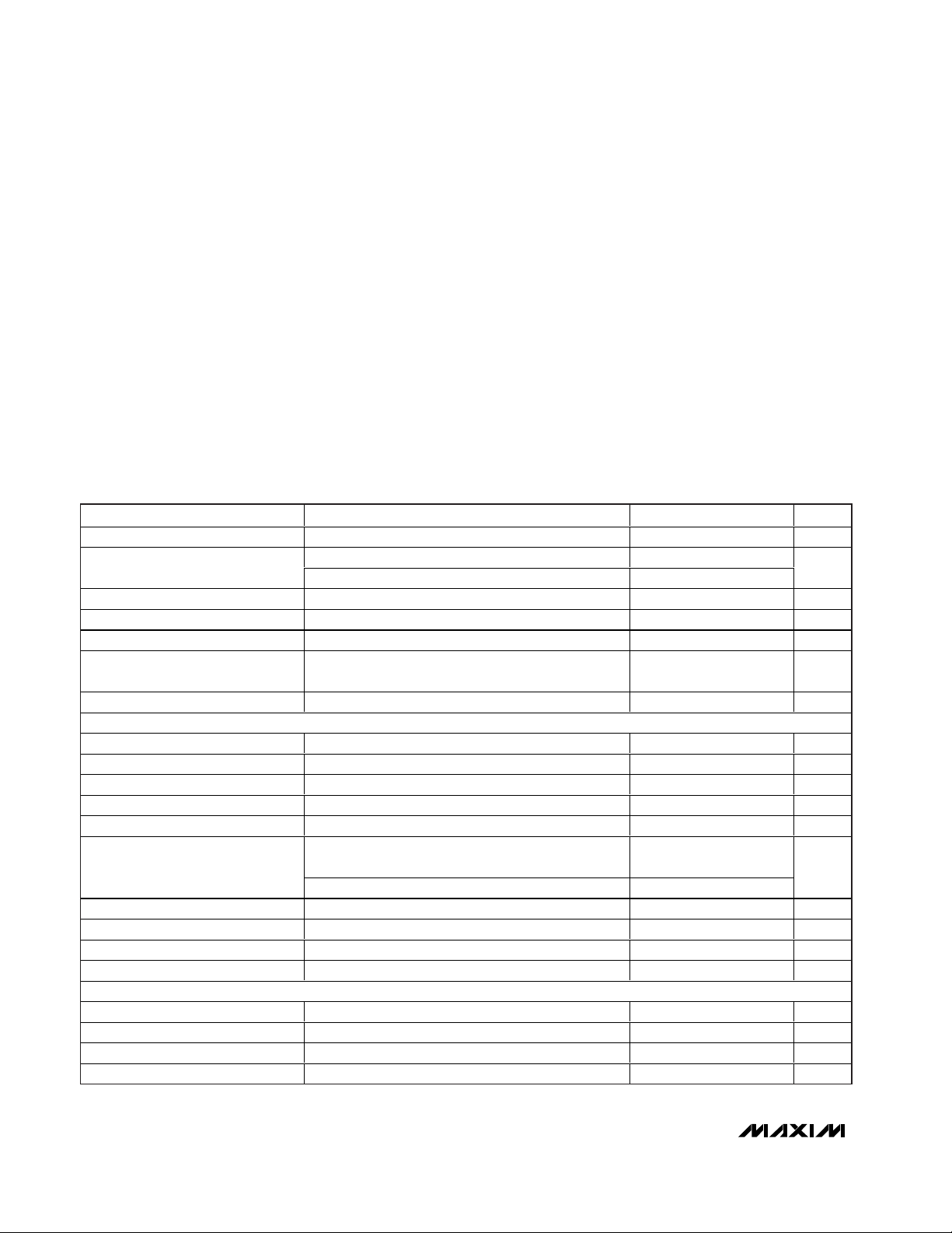
Figures 1, 2, and 3 are the Typical Operating Circuits of
the MAX8710, MAX8711, and MAX8712 for generating
power rails in TFT LCD panels. The input voltage range
is from 10.8V to 13.2V. The AVDD output is 10V at
300mA, the V
GON
output is 27V at 20mA, and the
V
GOFF
output is -5V at 50mA.
Detailed Description
The MAX8710/MAX8711/MAX8712 include a high-performance linear regulator, a positive charge-pump regulator, a negative charge-pump regulator, and built-in
power-up sequence control. The MAX8710 and
MAX8711 also include a high-current operational amplifier. Additionally, the MAX8710 provides logic-controlled
high-voltage switches to control the positive chargepump output. The linear regulator directly steps down the
input voltage to generate the source-driver ICs’ supply
voltage. The two built-in charge-pump regulators are
used to generate the TFT gate-on and gate-off supplies.
The high-current operational amplifier is typically used to
drive the LCD backplane (VCOM) and features high output current (150mA), fast slew rate (12V/µs), and wide
bandwidth (12MHz). Its rail-to-rail inputs and output maximize flexibility.
Linear Regulator
MAX8710/MAX8711/MAX8712 contain a linear regulator
that uses an internal PNP pass transistor to supply load
currents up to 300mA. Connect an external resistive voltage-divider between the regulator output and GND with
the midpoint connected to FBL to adjust the linear-regulator output. An error amplifier compares the FBL voltage
with the 2.5V internal reference voltage and amplifies the
difference. If the feedback voltage is higher than the
MAX8710 MAX8711 MAX8712
Page 11

MAX8710/MAX8711/MAX8712
Low-Cost Linear-Regulator
LCD Panel Power Supplies
______________________________________________________________________________________ 11
POSB
AVDD
OUTB
120kΩ
MMBD4148SE
(FAIRCHILD)
MMBD4148SE
(FAIRCHILD)
MMBD4148SE
(FAIRCHILD)
0.22µF
0.47µF
51.1kΩ
20kΩ
1µF
R5
110kΩ
1%
R6
100kΩ
1%
100kΩ
OUTB
DRVN
FBN
NEGB
OUTL
AVDD
10V/300mA
VP
27V/20mA
IN
GND
GND
IN
10.8V TO 13.2V
IN
0.1µF
10µF
4.7µF
0.1µF
0.1µF
1µF
0.1µF
100kΩ
0.1µF
R3
325kΩ
1%
0.1µF
20kΩ
GON
CTL
0.1µF
0.1µF
C1
47pF
R2
33.2kΩ
1%
R4
33.2kΩ
1%
R1
100kΩ
1%
GOFF
-5V/mA
REF
5V/1mA
SHDN
SUPB
MAX8710
N.C.
INL
REF
THR
MODE
SHDN DLP
CTL
DRN
GON
SRC
FBP
DRVP
SUPCP
FBL
Figure 1. Typical Operating Circuit of the MAX8710
Page 12

MAX8710/MAX8711/MAX8712
Low-Cost Linear-Regulator
LCD Panel Power Supplies
12 ______________________________________________________________________________________
POSB
AVDD
OUTB
120kΩ
MMBD4148SE
(FAIRCHILD)
MMBD4148
2x MMBD4148SE
(FAIRCHILD)
0.22µF
0.47µF
1µF
R5
110kΩ
1%
R6
100kΩ
1%
100kΩ
OUTB
DRVN
FBN
NEGB
OUTL
AVDD
10V/300mA
GON
27V/20mA
GND
GND
IN
10.8V TO 13.2V
IN
0.1µF
10µF
4.7µF
0.1µF
1µF
0.1µF
R3
325kΩ
1%
0.1µF
0.1µF
C1
47pF
R2
33.2kΩ
1%
R4
33.2kΩ
1%
R1
100kΩ
1%
GOFF
-5V/50mA
REF
5V/1mA
SHDN
SUPB
MAX8711
INL
REF
SHDN
DLP
FBP
DRVP
FBL
1µF
0.1µF
Figure 2. Typical Operating Circuit of the MAX8711
Page 13

MAX8710/MAX8711/MAX8712
Low-Cost Linear-Regulator
LCD Panel Power Supplies
______________________________________________________________________________________ 13
MMBD4148SE
(FAIRCHILD)
MMBD4148
2x MMBD4148SE
(FAIRCHILD)
0.22µF
0.47µF
1µF
R5
110kΩ
1%
R6
100kΩ
1%
DRVN
FBN
OUTL
AVDD
10V/300mA
GON
27V/20mA
GND
GND
IN
10.8V TO 13.2V
IN
0.1µF
10µF
4.7µF
1µF
0.1µF
R3
325kΩ
1%
0.1µF
0.1µF
C1
47pF
R2
33.2kΩ
1%
R4
33.2kΩ
1%
R1
100kΩ
1%
GOFF
-5V/50mA
REF
5V/1mA
SHDN
MAX8712
INL
REF
DLP
SHDN
FBP
DRVP
FBL
1µF
0.1µF
Figure 3. Typical Operating Circuit of the MAX8712
reference voltage, the controller lowers the base current
of the PNP transistor, which reduces the amount of current delivered to the output. If the feedback voltage is too
low, the device increases the PNP transistor’s base current, which allows more current to pass to the output and
raises the output voltage. The linear regulator also
includes an output current limit that protects the internal
pass transistor against short circuits.
The input voltage range of the linear regulator is from 8V
to 28V. The Typical Operating Circuits shown use a 12V
input. The output voltage range of the linear regulator
(OUTL) is up to 28V (MAX8710) or up to 14V
(MAX8711/MAX8712). The linear-regulator output is used
to generate the AVDD voltage, which is the analog supply
rail for source-driver ICs in TFT LCD panels. The typical
load of the AVDD supply is a periodic pulsed load, with a
peak current of approximately 1A and pulse width of
approximately 2µs. The period of the pulse load is
between 8.9µs and 31.7µs. The excellent transient performance of the linear regulator can easily meet this transient-response requirement.
The linear regulator can deliver at least 300mA output
current continuously with a 4.7µF output capacitor. Do not
allow the device power dissipation to exceed the package-dissipation limit listed in the Absolute Maximum
Ratings section. The power dissipation can be estimated
by multiplying the voltage difference between the input
and the output with the required maximum continuous
output current. For applications where the power dissipation exceeds the package limit, see the External
Transistor for Higher Current or Power Dissipation section
for more information.
The linear regulator is enabled whenever REF is in regulation and SHDN is logic high. Each time it is enabled, the
Page 14

MAX8710/MAX8711/MAX8712
Low-Cost Linear-Regulator
LCD Panel Power Supplies
14 ______________________________________________________________________________________
FBN
DRVN
DLP
POSB
SUPB
OUTB
NEGB
MODE
CTL
REF
VGOFF
AVDD
VCOM
CTL
AVDD
VIN
SUPCP
INL
OUTL
FBL
AVDD
VP
IN
GND
IN
REF
REF
MAX8710
SHDN
DRVP
FBP
SRC
REF
VGON
GON
DRN
THR
LINEAR
REG
SEQ
SWITCH
CONTROL
OSC
Figure 4. MAX8710 Functional Diagram
Page 15

MAX8710/MAX8711/MAX8712
Low-Cost Linear-Regulator
LCD Panel Power Supplies
______________________________________________________________________________________ 15
REF
V
SUPCP
FBN
250mV
0.5 x V
REF
SUPCP
DRVN
V
NEG
C
OUT(NEG)
C
X(NEG)
D3
D4
C
X(POS)
V
SUPCP
V
POS
C
OUT(POS)
D2
D1
DRVP
FBP
P2
N2
P1
N1
SEQUENCE
OSCILLATOR
MAX8710
Figure 5. Charge-Pump Regulator Functional Diagram
linear regulator goes through a soft-start routine by ramping up its internal reference voltage from 0 to 2.5V in 128
steps. The soft-start period is 2.73ms (typ), and FBL fault
detection is disabled during this period. This soft-start
feature effectively limits the inrush current during startup.
The linear-regulator current-limit circuitry monitors the
current flowing through the internal pass transistor. The
internal current limit is approximately 800mA. The linearregulator output declines when it is not able to supply the
load current. If the FBL voltage drops below 0.75V, the
current limit folds back to approximately 100mA.
The MAX8710/MAX8711/MAX8712 monitor the FBL voltage for undervoltage conditions. If V
FBL
is continuously
below 2V (typ) for approximately 44ms, the device latches off. The foldback current-limit circuit, in conjunction
with the output undervoltage fault latch and thermal-overload protection, protects the output load and the internal
pass transistor against short circuits or overloads.
Positive Charge-Pump Regulator
The positive charge-pump regulator is typically used to
generate the positive supply rail for the TFT LCD gate-driver ICs. The output voltage is set with an external resistive
voltage-divider from its output to GND with the midpoint
connected to FBP. The number of charge-pump stages
and the setting of the feedback divider determine the output voltage of the positive charge-pump regulator. The
charge pump includes a high-side P-channel MOSFET
(P1) and a low-side N-channel MOSFET (N1) to control
the power transfer as shown in Figure 5. The MOSFETs
switch at a constant frequency of 1.5MHz.
During the first half-cycle, N1 turns on and allows V
INPUT
(V
SUPCP
, MAX8710 or VOUTL, MAX8711/MAX8712) to
charge up the flying capacitor C
X(POS)
through diode
D1. The amount of charge transferred from V
INPUT
to
C
X(POS)
is determined by the on-resistance of N1, which
varies according to the output of the feedback error
amplifier. The error amplifier compares the feedback signal (FBP) with a 2.5V internal reference and amplifies the
difference. If the feedback signal is below the reference,
the error-amplifier output increases the supply voltage of
N1’s gate driver, lowering the on-resistance. Similarly, if
the feedback signal is above the reference, the erroramplifier output reduces the driver supply voltage,
increasing the on-resistance. During the second halfcycle, N1 turns off and P1 turns on, level shifting C
X(POS)
by V
INPUT
volts. This connects C
X(POS)
in parallel with
the reservoir capacitor C
OUT(POS)
. If the voltage
across C
OUT(POS)
plus a diode drop (V
POS
+ V
DIODE
) is
smaller than the level-shifted flying-capacitor voltage
Page 16

(V
CX(POS)
+ V
INPUT
), charge flows from C
X(POS)
to
C
OUT(POS)
until diode D2 turns off.
The positive charge-pump regulator’s startup can be
delayed by connecting an external capacitor from DLP
to GND. An internal constant current source begins
charging the DLP capacitor when SHDN is logic high
and REF reaches regulation. When the DLP voltage
exceeds V
REF
/ 2, the positive charge-pump regulator
is enabled. Each time it is enabled, the positive chargepump regulator goes through a soft-start routine by
ramping up its internal reference voltage from 0 to 2.5V
in 128 steps. The soft-start period is 2.73ms (typ), and
FBP fault detection is disabled during this period. The
soft-start feature effectively limits the inrush current during startup. The MAX8710/MAX8711/MAX8712 also
monitor the FBP voltage for undervoltage conditions. If
V
FBP
is continuously below 2V (typ) for approximately
44ms, the device latches off.
Negative Charge-Pump Regulator
The negative charge-pump regulator is typically used to
generate the negative supply rail for the TFT LCD gatedriver ICs. The output voltage is set with an external resistive voltage-divider from its output to REF with the midpoint connected to FBN. The number of charge-pump
stages and the setting of the feedback divider determine
the output of the negative charge-pump regulator. The
charge-pump controller includes a high-side P-channel
MOSFET (P2) and a low-side N-channel MOSFET (N2) to
control the power transfer as shown in Figure 5. The
MOSFETs switch a constant frequency of 1.5MHz.
During the first half-cycle, P2 turns on and allows
V
INPUT
to charge up the flying capacitor C
X(NEG)
through diode D3. During the second half-cycle, P2
turns off and N2 turns on, level shifting C
X(NEG)
by V
IN-
PUT
volts. This connects C
X(NEG)
in parallel with reser-
voir capacitor C
OUT(NEG)
. If the voltage across
C
OUT(NEG)
minus a diode drop is greater than the volt-
age across C
X(NEG)
, charge flows from C
OUT(NEG)
to
C
X(NEG)
until the diode D4 turns off. The amount of
charge transferred to the output is controlled by the onresistance of N2, which varies according to the output
of the feedback error amplifier. The error amplifier compares the feedback signal (FBN) with a 250mV internal
reference and amplifies the difference. If the feedback
signal is above the reference, the error-amplifier output
increases the supply voltage of N2’s gate driver, lowering the on-resistance. Similarly, if the feedback signal is
below the reference, the error-amplifier output reduces
the driver supply voltage, increasing the on-resistance.
The negative charge-pump regulator is enabled when
SHDN is logic high and REF reaches regulation. Each
time it is enabled, the negative charge-pump regulator
goes through a soft-start routine by ramping down its
internal reference voltage from 5V to 250mV in 128
steps. The soft-start period is 2.73ms (typ), and FBN
fault detection is disabled during this period. The softstart feature effectively limits the inrush current during
startup. The MAX8710/MAX8711/MAX8712 also monitor
the FBN voltage for undervoltage conditions. If V
FBN
is
continuously above 700mV (typ) for approximately
44ms, the device latches off.
Operational Amplifier
(MAX8710/MAX8711)
The MAX8710/MAX8711s’ operational amplifier features
high output current (150mA), fast slew rate (7.5V/µs),
and wide bandwidth (12MHz). The operational amplifier
is enabled when REF is in regulation and SHDN is logic
high. The output of the amplifier (OUTB) is internally
pulled to ground through a 1kΩ resistor in shutdown.
The amplifier is typically used to drive the backplane
(VCOM) of TFT LCD panels. The LCD backplane
consists of a distributed series capacitance and resistance, a load that can be easily driven by this operational amplifier. However, if the operational amplifier is
used in an application with a pure capacitive load,
steps must be taken to ensure stable operation. As the
operational amplifier’s capacitive load increases, the
amplifier’s bandwidth decreases and its gain peaking
increases. To ensure stable operation, a 5Ω to 50Ω
resistor can be placed between OUTB and the capacitive load to reduce gain peaking.
The operational amplifier limits short-circuit current to
approximately ±150mA if the output is directly shorted
to SUPB or to GND. If the short-circuit condition
persists, the junction temperature of the IC rises until it
trips the IC’s thermal-overload protection.
Reference Voltage (REF)
The reference output is nominally 5V and can source
up to 1mA (see the Typical Operating Characteristics).
Bypass REF with a 0.22µF ceramic capacitor connected between REF and GND. The reference remains
enabled in shutdown.
Power-Up Sequence and Shutdown Control
When the MAX8710/MAX8711/MAX8712 are powered
up, REF rises with the voltage on IN. After REF reaches
regulation and if SHDN is logic high, the linear regulator, operational amplifier, and negative charge-pump
regulator are enabled and begin their respective softstart routines. After the soft-start routines are complet-
MAX8710/MAX8711/MAX8712
Low-Cost Linear-Regulator
LCD Panel Power Supplies
16 ______________________________________________________________________________________
Page 17

MAX8710/MAX8711/MAX8712
Low-Cost Linear-Regulator
LCD Panel Power Supplies
______________________________________________________________________________________ 17
ed, the fault-protection circuits for the linear regulator
and the negative charge-pump regulator are activated.
When the linear regulator is enabled, the positive
charge-pump-regulator delay block is enabled. An
internal current source starts charging the DLP capacitor. The voltage on DLP linearly rises because of the
constant charging current. When V
DLP
goes above
V
REF
/ 2, the switch control block is enabled, and the
positive charge-pump regulator begins its soft-start.
After the positive charge-pump regulator’s soft-start is
completed, the fault protection of the positive chargepump regulator is also enabled.
The MAX8710/MAX8711/MAX8712 enter into shutdown
when SHDN is pulled low or REF falls below 4.5V. In
shutdown, OUTL, GON and OUTB are all internally
pulled to ground with 1kΩ resistors. FBN, FBP, and DLP
are all internally pulled to ground with 10Ω resistors in
shutdown. The DLP current source is disabled in shutdown and a switch discharges C
DLP
to ground. REF
remains on in shutdown. Pulling SHDN high when REF
is above 4.5V reactivates the IC. Output fault protection
and thermal-overload protection can also turn off the
IC’s outputs. See the respective sections for details.
Output Fault Protection
During steady-state operation, if the output of the linear
regulator or any of the charge-pump regulator outputs
does not exceed its respective fault-detection threshold, the MAX8710/MAX8711/MAX8712 activate an internal fault timer. If any condition or the combination of
conditions indicates a continuous fault for the faulttimer duration (44ms typ), the MAX8710/MAX8711/
MAX8712 set the fault latch, shutting down all the outputs except the reference. Once the fault condition is
removed, cycle the input voltage or toggle SHDN to
clear the fault latch and reactivate the device. Each
regulator’s fault-detection circuit is disabled during the
regulator’s soft-start time.
Thermal-Overload Protection
The thermal-overload protection prevents excessive
power dissipation from overheating the IC. When the
junction temperature exceeds +160°C, a thermal sensor
immediately activates the fault protection, which shuts
down all the outputs except the reference, allowing the
device to cool down. Once the device cools down by
approximately 15°C, the IC restarts automatically.
Switch Control (MAX8710)
The MAX8710’s switch-control block (Figure 6) consists
of a high-voltage P-channel MOSFET Q1 between SRC
and GON, and a common-source-connected P-channel
MOSFET pair Q2 between GON and DRN. The switchcontrol block is enabled when V
DLP
goes above V
REF
/
2. Q1 and Q2 are controlled by CTL and MODE. There
are two different modes of operation.
Activate the first mode by connecting MODE to REF.
When CTL is logic high, Q1 turns on and Q2 turns off,
connecting GON to SRC. When CTL is logic low, Q1
turns off and Q2 turns on, connecting GON to DRN.
GON can then be discharged through a resistor connected between DRN and GND or OUTL. Q2 turns off
and stops discharging GON when V
GON
reaches 10
times the voltage on THR.
When V
MODE
is less than 0.9 x V
REF
, the switch-control
block works in the second mode. The rising edge of V
CTL
turns on Q1 and turns off Q2, connecting GON to SRC.
An internal N-channel MOSFET Q5 between MODE and
GND is also turned on to discharge an external capacitor
between MODE and GND. The falling edge of V
CTL
turns
off Q5, and an internal 50µA current source starts charging the MODE capacitor. Once V
MODE
exceeds 0.5 x
V
REF
, the switch-control block turns off Q1 and turns on
Q2, connecting GON to DRN. GON can then be discharged through a resistor connected between DRN and
GND or OUTL. Q2 turns off and stops discharging GON
when V
GON
reaches 10 times the voltage on THR.
Page 18

MAX8710/MAX8711/MAX8712
Low-Cost Linear-Regulator
LCD Panel Power Supplies
18 ______________________________________________________________________________________
REF
1kΩ
9R
R
Q3
Q2
SRC
GON
DRN
THR
Q1
5µA
50µA
REF
R
4R
5R
1kΩ
Q5
CTL
MODE
Q4
0.5 x V
REF
DLP
FAULT
SHDN
REF OK
MAX8710
Figure 6. MAX8710 High-Voltage Switch Control
Page 19

Design Procedure
Linear Regulator
Output-Voltage Selection
Adjust the linear-regulator output voltage by connecting
a resistive voltage-divider from the linear-regulator output AVDD to GND with the center tap connected to FBL
(Figure 1). Select the lower resistor of the divider R2 in
the range of 10kΩ to 50kΩ. Calculate the upper resistor
R1 with the following equation:
where V
FBL
= 2.5V (typ) is the regulation point of the
linear regulator.
Input-Capacitor Selection
The linear regulator’s output stage consists of a PNP pass
transistor. Rapid movements of the input voltage must be
avoided since the movement can be coupled into the
base of the transistor through the base-to-emitter junction
capacitance. The input capacitor reduces the current
peaks drawn from the input supply and slows down the
input voltage movement. One 10µF ceramic capacitor is
used in the Typical Operating Circuits (Figure 1, 2, and 3)
because of the high source impedance seen in typical
lab setups. Actual applications usually have much lower
source impedance, since the linear regulator typically
runs directly from the output of another regulated supply
and can operate with less input capacitance.
Output-Capacitor Selection
The output capacitor and its equivalent series resistance
(ESR) affect the linear regulator’s stability and transient
response. The regulator can deliver at least 300mA output current continuously with a 4.7µF output capacitor.
The typical load on the linear regulator for source-driver
applications is a large pulsed load, with a peak current
of approximately 1A and pulse width of approximately
2µs. The shape of the pulse is close to a triangle, so it
is equivalent to a square pulse with 1A height and 1µs
pulse width. The total voltage dip during the pulsed
load transient also has two components: the ohmic dip
due to the output capacitor’s ESR, and the capacitive
dip caused by discharging the output capacitance:
where I
PULSE
is the height of the pulse load, and t
PULSE
is the pulse width. Higher capacitance and lower ESR
result in less voltage dip. The ESR dip can be ignored
when using ceramic output capacitors. Calculate the
minimum required capacitance for the maximum allowed
dip using:
The above equations are “worst-case” and assume that
the linear regulator does not react to correct the output
voltage during the load pulse. In fact, the regulator is
fast enough to partially correct the output voltage, so
the actual dip may be smaller, or a smaller capacitor
may be acceptable. For the typical load pulse
described above, assuming the voltage dip must be
limited to 150mV, the minimum output capacitor is:
Because the regulator is able to limit the dip somewhat,
the circuit of Figure 1 uses a 4.7µF output capacitor.
The voltage rating and temperature characteristics of
the output capacitor must also be considered.
Feed-Forward Compensation
The output capacitance and equivalent load resistance
determine the dominant pole. An internal parasitic
capacitance of the regulator creates a second pole.
This pole typically occurs at 100kHz, but can vary
between 60kHz and 140kHz depending on the process
variation. Since the pole occurs after the loop gain
crossover, it does not affect the loop stability. However,
canceling this pole with an additional zero can improve
the load-transient response.
A zero can be added by connecting a feed-forward
capacitor (C1) between OUTL and FBL as shown in
Figure 1. The frequency of the zero can be calculated
with the following equation:
where R1 is the upper resistor of the feedback divider.
To cancel the second pole, the zero should be placed
at or below the frequency of the second pole. Because
the frequency of the second pole varies between
60kHz and 140kHz, the zero can be placed between
40kHz and 60kHz.
f
RC
ZERO
=
××
1
211π
C
As
V
F
OUT MIN()
.
.≈
×
=
11
015
67µµ
C
It
V
OUT MIN
PULSE PULSE
DIP MAX
()
()
≈×
VV V
VIR
V
It
C
DIP DIP ESR DIP C
DIP ESR PULSE ESR
DIP C
PULSE PULSE
OUT
() ()
()
()
=+
=×
≈
×
RR
V
V
AVDD
FBL
12 1 =×
−
MAX8710/MAX8711/MAX8712
Low-Cost Linear-Regulator
LCD Panel Power Supplies
______________________________________________________________________________________ 19
Page 20

MAX8710/MAX8711/MAX8712
Low-Cost Linear-Regulator
LCD Panel Power Supplies
20 ______________________________________________________________________________________
Charge-Pump Regulators
Number of Charge-Pump Stages
For highest efficiency, always choose the lowest number of charge-pump stages that meets the output
requirement.
The number of positive charge-pump stages is given by:
where n
POS
is the number of positive charge-pump
stages, VPis the positive charge-pump regulator output, V
INPUT
is the supply voltage for the charge-pump
regulators (V
SUPCP
, MAX8710 or V
OUTL
, MAX8711/
MAX8712), V
DIODE
is the forward-voltage drop of the
charge-pump diode, and V
SWITCH
is the voltage drop
of the internal switches. Use V
SWITCH
= 0.3V.
The number of negative charge-pump stages is given by:
where n
NEG
is the number of negative charge-pump
stages and V
GOFF
is the negative charge-pump regula-
tor output.
The above equations are derived based on the
assumption that the first stage of the positive charge
pump is connected to V
MAIN
and the first stage of the
negative charge pump is connected to ground.
Sometimes fractional stages are more desirable for better efficiency. This can be done by connecting the first
stage to another available supply, such as a 5V supply.
If the first charge-pump stage is powered from 5V, then
the above equations become:
Output Voltage Selection
Adjust the positive charge-pump-regulator output voltage by connecting a resistive voltage-divider from the
regulator output VPto GND with the center tap connected to FBP (Figure 1). Select the lower resistor of divider
R4 in the range of 10kΩ to 50kΩ. Calculate upper resistor
R3 with the following equation:
where V
FBP
= 2.5V (typ) is the regulation point of the
positive charge-pump regulator.
Adjust the negative charge-pump-regulator output volt-
age by connecting a resistive voltage-divider from the
negative charge-pump output V
GOFF
to REF with the
center tap connected to FBN (Figure 1). Select R6 in
the 20kΩ to 100kΩ range. Calculate R5 with the following equation:
where V
REF
= 5V and V
FBN
= 250mV is the regulation
point of the negative charge-pump regulator.
Flying Capacitor
Increasing the flying-capacitor (CX) value lowers the
effective source impedance and increases the outputcurrent capability of the charge pump. Increasing the
capacitance indefinitely has a negligible effect on output-current capability because the internal switch resistance and the diode impedance place a lower limit on
the source impedance. A 0.1µF ceramic capacitor
works well in most low-current applications. The flying
capacitor’s voltage rating must exceed the following:
VCX> n x V
INPUT
where n is the stage number in which the flying capacitor is used, and V
INPUT
is the supply voltage for the
charge-pump regulators (V
SUPCP
, MAX8710 or V
OUTL
,
MAX8711/MAX8712).
Charge-Pump Input Capacitor
Use an input capacitor with a value equal to or greater
than the flying capacitor. Place the capacitor as close
to the IC as possible. Connect the capacitor directly
to PGND.
RR
VV
VV
FBN GOFF
REF FBN
56
=×
−
−
RR
V
V
P
FBP
34 1 =×
−
n
VV V
VV
n
VV V
VV
POS
PSWITCH
INPUT DIODE
NEG
GOFF SWITCH
INPUT DIODE
=
+
×
=
++
×
−
−
−
−
5
2
5
2
n
VV
VV
NEG
GOFF SWITCH
INPUT DIODE
=
+
×
−
−
2
n
VV V
VV
POS
PSWITCH SUPCP
INPUT DIODE
=
+
×
−
−
2
Page 21

Charge-Pump Output Capacitor
Increasing the output capacitance or decreasing the
ESR reduces the output ripple voltage and the peak-topeak transient voltage. With ceramic capacitors, the
output voltage ripple is dominated by the capacitance
value. Use the following equation to approximate the
required capacitor value:
where C
OUT_CP
is the output capacitor of the charge
pump, I
LOAD_CP
is the load current of the charge
pump, and V
RIPPLE_CP
is the desired peak-to-peak
value of the output ripple.
Charge-Pump Rectifier Diode
Use low-cost silicon switching diodes with a current rating equal to or greater than two times the average
charge-pump input current. If it helps avoid an extra
stage, some or all of the diodes can be replaced with
Schottky diodes with an equivalent current rating.
Applications Information
External Transistor for Higher Current
or Power Dissipation
The load current and the voltage difference between
the input and output determine the linear regulator’s
power dissipation as shown in the following equation:
P
DISSIPATION
= (V
INL
- V
OUTL
) x I
OUTL
For some applications, the input voltage to the linear
regulator is from a 19V adapter. To make a 10V output,
the voltage across the pass transistor is 9V. In this case,
the regulator’s power dissipation may exceed the dissipation limit that the package can handle. In some other
applications, the load current may be much higher than
the regulator’s guaranteed 300mA output current.
The solution for such applications is to connect an external PNP transistor with the internal PNP transistor in a
Darlington configuration as shown in Figure 7. The
external pass transistor must be able to handle most of
the power dissipation since most of the load current
flows through it. On the other hand, the power dissipated in the internal pass transistor is very low. The currentlimit circuit will not work if an external pass transistor is
used because the linear regulator only senses the current of the internal pass transistor.
Using the MAX1512 VCOM Calibrator
to Adjust the Buffer Output
The operational amplifier is typically used as the VCOM
buffer in TFT LCD panels. The output voltage of the
VCOM buffer can be adjusted using the MAX1512,
which is an EEPROM-programmable VCOM calibrator,
using the circuit shown in Figure 8. Refer to the
MAX1512 data sheet for details.
C
I
fV
OUT CP
LOAD CP
OSC RIPPLE CP
_
_
_
≥
2
MAX8710/MAX8711/MAX8712
Low-Cost Linear-Regulator
LCD Panel Power Supplies
______________________________________________________________________________________ 21
MAX8710
MAX8711
MAX8712
LINEAR
REGULATOR
4.7µF
4.7µF
INL
OUTL
FBL
V
IN
= 19V
KSB834W
(FAIRCHILD)
AVDD = 10V
51Ω
140kΩ
20kΩ
Figure 7. High-Power Linear Regulator
MAX8710
MAX8711
REF
V
DD
GND
OUTL
CE
AVDD
OUT
SET
CTL
OUTB
TO
VCOM
SUPB
POSB
NEGB
20kΩ
0.47µF
4.7µF
0.1µF
100kΩ
25kΩ
MAX1512
Figure 8. Using the MAX1512 to Adjust the VCOM Buffer Output
Page 22

PC Board Layout Guidelines
Careful PC board layout is important for proper operation. Use the following guidelines for good PC board
layout:
1) Create a power ground island consisting of the linear-regulator input and output-capacitor ground
connections, the GND pin, and the capacitor
ground connections for the charge-pump regulators. Connect all these together with short, wide
traces or a small ground plane. Maximizing the
width of the power ground traces improves efficiency. Create an analog ground island consisting of all
the feedback-divider ground connections, the operational-amplifier divider ground connection, the REF
capacitor ground connection, the MODE capacitor
ground connection, the DLP capacitor ground connection, and the device’s exposed backside pad.
Connect the analog ground island and the power
ground island by connecting the GND pin directly to
the exposed backside pad. Make no other connections between these separate ground islands.
2) Place all feedback voltage-divider resistors as close
to their respective feedback pins as possible. The
divider’s center trace should be kept short. Placing
the resistors far away causes their FB traces to
become antennas that can pick up noise from the
switching nodes of the charge pumps. Avoid running
any feedback trace near these switching nodes.
3) Place IN, INL, SUPB, SUPCP, and REF pin bypass
capacitors close to the IC. The ground connection
of the IN bypass capacitor should be connected
directly to the GND pin with a wide trace.
4) Minimize the length and maximize the width of the
traces between the output capacitors and the load
for best transient responses.
5) Minimize the size of the switching nodes (DRVP and
DRVN). Keep the switching nodes away from feedback nodes (FBL, FBP, and FBN) and the analog
ground. Use DC traces as a shield if necessary.
Refer to the MAX8710 evaluation kit for an example of
proper board layout.
Pin Configurations (continued)
MAX8710/MAX8711/MAX8712
Low-Cost Linear-Regulator
LCD Panel Power Supplies
22 ______________________________________________________________________________________
16
1
2
3
4
12
11
10
9
15 14 13
5678
FBN
FBN
OUTL
DRVN
DRVP
DLP
FBL
DLP
FBL
SHDN
FBP
SUPB
OUTB
GND
POSB
INL
NEGB
IN
OUTL
DRVN
DRVP
REF
TOP VIEW
MAX8711
THIN QFN 4mm x 4mm
12 11
10
456
1
2INL
3
9
8
7IN
FBP
SHDN
GND
MAX8712
REF
THIN QFN 4mm x 4mm
Chip Information
TRANSISTOR COUNT: 3946
PROCESS: BiCMOS
Page 23

MAX8710/MAX8711/MAX8712
Low-Cost Linear-Regulator
LCD Panel Power Supplies
Maxim cannot assume responsibility for use of any circuitry other than circuitry entirely embodied in a Maxim product. No circuit patent licenses are
implied. Maxim reserves the right to change the circuitry and specifications without notice at any time.
Maxim Integrated Products, 120 San Gabriel Drive, Sunnyvale, CA 94086 408-737-7600 ____________________ 23
© 2004 Maxim Integrated Products Printed USA is a registered trademark of Maxim Integrated Products.
Package Information
(The package drawing(s) in this data sheet may not reflect the most current specifications. For the latest package outline information
go to www.maxim-ic.com/packages
.)
24L QFN THIN.EPS
PACKAGE OUTLINE
12,16,20,24L QFN THIN, 4x4x0.8 mm
21-0139
1
B
2
PACKAGE OUTLINE
12,16,20,24L QFN THIN, 4x4x0.8 mm
21-0139
2
B
2
 Loading...