

Page 1
For free samples & the latest literature: http://www.maxim-ic.com, or phone 1-800-998-8800.
For small orders, phone 408-737-7600 ext. 3468.
General Description
The MAX868 inverting charge pump provides a low-cost
and compact means of generating a regulated negative
voltage up to -2 x VINfrom a positive input voltage
between 1.8V and 5.5V. It uses a pulse-frequencymodulation (PFM) control scheme to generate the regulated negative output voltage. PFM operation is obtained
by gating the internal 450kHz oscillator on and off as
needed to maintain output voltage regulation. This
unique on-demand switching scheme gives the MAX868
excellent light-load efficiency without degrading its fullload operation (up to 30mA), permitting smaller capacitors to take advantage of the oscillator’s high switching
frequency.
The MAX868 requires no inductors; only four capacitors
are required to build a complete DC-DC converter.
Output voltage regulation is achieved by adding just two
resistors. The MAX868 comes in a 10-pin µMAX package, which is only 1.11mm high and occupies just half
the board area of a standard 8-pin SO.
________________________Applications
Small LCD Panels
Cell Phones
Cordless Phones
Camcorders
Handy-Terminals, PDAs
Medical Instruments
Battery-Operated Equipment
____________________________Features
♦ Regulated Negative Output Voltage
(up to -2 x VIN)
♦ Ultra-Small, 10-Pin µMAX Package
♦ On-Demand Switching at up to 450kHz
♦ 30µA Quiescent Supply Current
♦ Requires Only Four Small External Capacitors
♦ 1.8V to 5.5V Input Voltage Range
♦ 0.1µA Logic-Controlled Shutdown
♦ Up to 30mA Output Current
MAX868
Regulated, Adjustable -2x
Inverting Charge Pump
________________________________________________________________
Maxim Integrated Products
1
1
2
3
4
5
10
9
8
7
6
FB
SHDN
C2+
INPGND
C1-
OUT
GND
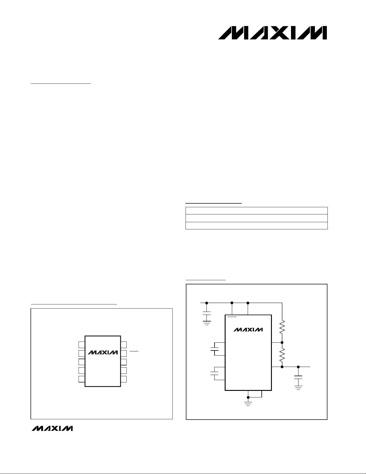
MAX868
µMAX
TOP VIEW
C2-C1+
Configuration
MAX868
C1+
IN
PGND
SHDN
GND
FB
OUT
0.1µF
1µF
2.2µF
V
OUT
= 0V TO -2 x V
IN
V
IN
= 1.8V TO 5.5V
0.1µF
C1-
C2+
C2-
Typical Operating Circuit
19-1290; Rev 1; 2/98
PART
MAX868C/D
MAX868EUB -40°C to +85°C
0°C to +70°C
TEMP. RANGE PIN-PACKAGE
Dice*
10 µMAX
Ordering Information
*
Dice are tested at TA= +25°C.
Page 2
MAX868
Regulated, Adjustable -2x
Inverting Charge Pump
2 _______________________________________________________________________________________
ABSOLUTE MAXIMUM RATINGS
ELECTRICAL CHARACTERISTICS
(VIN= +3.3V, SHDN = IN, C1 = C2 = 0.22µF, CIN= 1µF, C
OUT
= 10µF, TA= 0°C to +85°C, unless otherwise noted. Typical values
are at T
A
= +25°C.)
Stresses beyond those listed under “Absolute Maximum Ratings” may cause permanent damage to the device. These are stress ratings only, and functional
operation of the device at these or any other conditions beyond those indicated in the operational sections of the specifications is not implied. Exposure to
absolute maximum rating conditions for extended periods may affect device reliability.
IN to GND.................................................................-0.3V to +6V
OUT to GND...........................................................+0.3V to -12V
IN to OUT.................................................................-0.3V to -17V
C1+ to GND........................................(V
IN
- 12V) to (VIN+ 0.3V)
C1- to GND.............................................................+0.3V to -12V
C2+ to GND....................................................(V
IN
+ 0.3V) to -6V
C2- to GND...............................................................+0.3V to -6V
SHDN, FB to GND .......................................-0.3V to (V
IN
+ 0.3V)
PGND to GND .......................................................-0.3V to +0.3V
Output Current....................................................................35mA
Short-Circuit Duration.................................................Continuous
Continuous Power Dissipation (T
A
= +70°C)
10-pin µMAX (derate 5.6mW/°C above +70°C)...........444mW
Operating Temperature Range
MAX868EUB....................................................-40°C to +85°C
Storage Temperature Range.............................-65°C to +160°C
Lead Temperature (soldering, 10sec).............................+300°C
FB = IN
No load, VFB= -50mV
RL= 3kΩ to GND
VIN= 5.5V, SHDN = IN or GND
VIN= 1.8V to 5.5V
SHDN = GND (OUT pulls to GND)
VIN= 1.8V to 5.5V, TA= +25°C
I
OUT
= 5mA, FB = IN
No load, SHDN = GND
VFB= 50mV
Closed loop
V
OUT
= -5V
CONDITIONS
nA-100 1 100
SHDN Input Bias Current
V
0.7V
IN
V
IH
SHDN Input Threshold
0.3V
IN
V
IL
nA-50 1 50FB Input Bias Current
mA
30
I
OUT
Output Current
12
mA5
I
IN
Supply Current
µA30 50
V1.8 5.5V
IN
Supply-Voltage Range
mV-30 30
15 50
R
OUT
Open-Loop Output
Resistance
Ω
125
70 100
µA0.1 1IIN,
SHDN
Shutdown Current
kHz
293 450 607
Oscillator Frequency
270 630
f
OSC
Ω0.2R
OUT,CL
Closed-Loop Output
Resistance
UNITSMIN TYP MAXSYMBOLPARAMETER
TA= +25°C
TA= 0°C to +85°C
TA= +25°C
TA= 0°C to +85°C
VIN= 3.3V, V
OUT
= -5V
VIN= 5V, V
OUT
= -3.3V
VIN= 1.8V to 5.5V
mV-40 40
FB Trip Point
TA= 0°C to +85°C
TA= +25°C
Page 3
MAX868
Regulated, Adjustable -2x
Inverting Charge Pump
_______________________________________________________________________________________ 3
ELECTRICAL CHARACTERISTICS
(VIN= +3.3V, C1 = C2 = 0.22µF, CIN= 1µF, C
OUT
= 10µF, TA= -40°C to +85°C, unless otherwise noted. (Note 1)
Note 1: Specifications to -40°C are guaranteed by design, not production tested.
RL= 3kΩ to GND
VFB= 50mV
No load, VFB= -50mV
No load, SHDN = GND
CONDITIONS
kHz270 630f
OSC
Oscillator Frequency
µA1I
IN,SHDN
Shutdown Current
V1.8 5.5V
IN
Supply-Voltage Range
µA55I
IN
Supply Current
UNITSMIN TYP MAXSYMBOLPARAMETER
I
OUT
= 5mA, FB = IN
VIN= 1.8V to 5.5V
SHDN = GND (OUT pulls to GND)
VIN= 1.8V to 5.5V
nA-100 100FB Input Bias Current
mV-40 40FB Trip Point
125
Open-Loop Output
Resistance
Ω
50
R
OUT
VIN= 5.5V, SHDN = IN or GND
VIN= 1.8V to 5.5V
nA-100 100
SHDN Input Bias Current
V
0.7V
IN
V
IH
SHDN Input Threshold
0.3V
IN
V
IL
__________________________________________Typical Operating Characteristics
(Circuit of Figure 5, TA= +25°C, unless otherwise noted.)
-35
-25
-30
-20
-5
0
-10
-15
5
0 10 15 20 255 30 35 40 45 50
LOAD-REGULATION ERROR
vs. LOAD CURRENT
(V
IN
= 5V)
MAX868-01
LOAD CURRENT (mA)
LOAD-REGULATION ERROR (mV)
V
OUT
= -7.5V
V
OUT
= -3.3V
V
OUT
= -5V
-15
-9
-12
0
-3
-6
3
0 5 10 15 20 25
LOAD-REGULATION ERROR
vs. LOAD CURRENT
(V
IN
= 3.3V)
MAX868-02
LOAD CURRENT (mA)
LOAD-REGULATION ERROR (mV)
V
OUT
= -3.3V
V
OUT
= -5V
400
410
430
440
420
480
470
460
450
500
490
-40 -20 0 20 40 60 80 100
MAXIMUM SWITCHING FREQUENCY
vs. TEMPERATURE
MAX868-03
TEMPERATURE (°C)
MAXIMUM SWITCHING FREQUENCY (kHz)
FB = IN
VIN = 3.3V
VIN = 2V
VIN = 5V
Page 4
MAX868
Regulated, Adjustable -2x
Inverting Charge Pump
4 _______________________________________________________________________________________
____________________________Typical Operating Characteristics (continued)
(Circuit of Figure 5, TA= +25°C, unless otherwise noted.)
0
0.01 10.1 10 100
EFFICIENCY vs. LOAD CURRENT
(V
IN
= 5V)
10
MAX868-04
LOAD CURRENT (mA)
EFFICIENCY (%)
50
40
30
20
60
70
80
V
OUT
= -5V
V
OUT
= -7.5V
V
OUT
= -3.3V
0
0.01 10.1 10 100
EFFICIENCY vs. LOAD CURRENT
(V
IN
= 3.3V)
10
MAX868-05
LOAD CURRENT (mA)
EFFICIENCY (%)
50
40
30
20
60
70
80
V
OUT
= -5V
V
OUT
= -3.3V
0
0.01 10.1 10 100
EFFICIENCY vs. LOAD CURRENT
(V
IN
= 5V)
10
MAX868-06
LOAD CURRENT (mA)
EFFICIENCY (%)
50
40
30
20
60
70
80
CIRCUIT OF FIGURE 6
V
OUT
= -2.5V
V
OUT
= -3.3V
0
60
40
20
100
80
180
160
140
120
200
-40 -20 0 20 40 60 80 100
OPEN-LOOP OUTPUT IMPEDANCE
vs. TEMPERATURE
(FB = IN, V
OUT
= -2 x VIN)
MAX868-07
TEMPERATURE (°C)
OUTPUT IMPEDANCE (Ω)
VIN = 2V
VIN = 3.3V
VIN = 5V
20µs/div
20mV/div
V
IN
= 3.3V, V
OUT
= -3.3V, I
LOAD
= 5mA,
V
OUT
AC COUPLED (20mV/div), C
OUT
= 10µF CERAMIC
OUTPUT VOLTAGE RIPPLE
(C
OUT
= 10µF CERAMIC)
MAX868-10
0
60
40
20
100
80
180
160
140
120
200
-40 -20 0 20 40 60 80 100
OPEN-LOOP OUTPUT IMPEDANCE
vs. TEMPERATURE
(FB = IN, V
OUT
= -VIN)
MAX868-08
TEMPERATURE (°C)
OUTPUT IMPEDANCE (Ω)
VIN = 2V
CIRCUIT OF FIGURE 6
VIN = 3.3V
VIN = 5V
20µs/div
20mV/div
V
IN
= 3.3V, V
OUT
= -3.3V, I
LOAD
= 5mA,
V
OUT
AC COUPLED (20mV/div), C
OUT
= 10µF (AVX TPS)
OUTPUT VOLTAGE RIPPLE
(C
OUT
= 10µF TANTALUM)
MAX868-09
20µs/div
20mV/div
V
IN
= 3.3V, V
OUT
= -3.3V, I
LOAD
= 5mA,
V
OUT
AC COUPLED (20mV/div), C
OUT
= 2.2µF CERAMIC
OUTPUT VOLTAGE RIPPLE
MAX868-11
200µs/div
10mA/div
20mV/div
V
IN
= 5V, V
OUT
= -5V, I
OUT
= 1mA TO 11mA STEP
LOAD-TRANSIENT RESPONSE
MAX868-12
Page 5

Detailed Description
The MAX868 inverting charge pump uses pulsefrequency-modulation (PFM) control to generate a regulated negative output voltage up to -2 x VIN. PFM
operation is obtained by enabling the internal 450kHz
oscillator as needed to maintain output voltage regulation. This control scheme reduces supply current at
light loads and permits the use of small capacitors.
The functional diagram shown in Figure 1 indicates the
two phases of MAX868 operation: charge phase (Φ1)
and discharge phase (Φ2). In charge phase, the
switches on the left-hand side close, and the switches
on the right-hand side open. In the discharge phase,
the inverse occurs.
Figure 2 illustrates that in charge phase, both flying
capacitors are charged in parallel. The load is serviced
entirely by the charge stored in the output capacitor.
Figure 3 demonstrates the series connection of the flying capacitors in the discharge phase. The series combination of the flying capacitors, when connected to the
output capacitor, transfers charge to the output in order
to maintain output voltage regulation. In normal operation, the MAX868 operates predominantly in charge
phase, switching to discharge phase only as needed to
maintain a regulated output.
MAX868
Regulated, Adjustable -2x
Inverting Charge Pump
_______________________________________________________________________________________ 5
Pin Description
Active-Low Shutdown Input. Connect SHDN to GND to put the MAX868 in shutdown mode and reduce supply current to 0.1µA. Connect to IN for normal operation. OUT is actively pulled to GND in shutdown.
SHDN
9
Feedback Input. Connect FB to a resistor divider for a regulated output voltage. Connect to IN to generate
an unregulated -2 x VINoutput voltage.
FB10
Positive Terminal of Flying Capacitor C1C1+5
Negative Terminal of Flying Capacitor C2C2-6
Supply-Voltage Input. Input voltage range is 1.8V to 5.5V.IN7
Positive Terminal of Flying Capacitor C2C2+8
Power GroundPGND4
Negative Terminal of Flying Capacitor C1C1-3
PIN
Charge-Pump OutputOUT2
Analog GroundGND1
FUNCTIONNAME
Figure 1. Functional Diagram
IN
Φ1 Φ2
SHDN
OSCILLATOR
C2+
C2C1+
C1-
OUT
FB
V
REF
C
OUT
Page 6

MAX868
__________________Design Procedure
Setting the Output Voltage
Set the output voltage using two external resistors, R1
and R2, as shown in Figure 4. Since the input bias current at FB has a 50nA maximum, large resistor values in
the feedback loop do not significantly degrade accuracy. Begin by selecting R2 in the 100kΩ to 500kΩ range,
and calculate R1 using the following equation:
where V
OUT
is the desired output voltage, and V
REF
is
any available regulated positive voltage. When the
MAX868 is powered by a regulated voltage, VINcan be
used as the reference for setting the output voltage.
When the MAX868 is powered by an unregulated supply, such as when operating directly from a battery, use
any available positive reference voltage in the system.
Note that due to the MAX868’s doubling and inverting
charge-pump action, the output voltage is limited to
-2 x V
IN
.
Alternatively, to configure the MAX868 as a simple,
unregulated doubler-inverter (V
OUT
= -2 x VIN), connect FB to IN. In this configuration, the MAX868 runs at
its maximum oscillator frequency, operating as a conventional, open-loop charge pump.
If multiple oscillator cycles are required to regulate the
output, reduce the values for R1 and R2, or parallel a
small capacitor (CC) across R1 to compensate the
feedback loop and ensure stability. Choose the lowest
capacitor value that ensures stability; values up to 47pF
are adequate for most applications.
R R x
V
V
OUT
REF
1 2
| |
=
Regulated, Adjustable -2x
Inverting Charge Pump
6 _______________________________________________________________________________________
C
OUT
V
OUT
C2C1+
C1-
C2+
IN
IN
GND
(a)
(b)
C
OUT
V
OUT
C2-
C2+
C1-
C1+
Figure 2. a) In charge phase, the left-hand switches are
closed and the right-hand switches are open, charging the flying capacitors (C1 and C2) while the output capacitor (C
OUT
)
services the load. b) The equivalent circuit of the charge phase
of operation.
C2C1+
C1-
C2+
IN
(a)
(b)
C
OUT
V
OUT
C
OUT
V
OUT
C2+
C2-
C1+
C1-
Figure 3. a) In discharge phase, the left-hand switches are
open and the right-hand switches are closed, transferring
energy from the flying capacitors (C1 and C2) to the output
capacitor (C
OUT
). b) The equivalent circuit of the discharge
phase of operation.
Page 7

Capacitor Selection
Choosing the Flying Capacitors
Proper choice of the flying capacitors is dependent primarily upon the desired output current. For flying capacitors in the 0.1µF to 0.33µF range, the maximum output
current can be approximated by the following equation:
where f
MAX
is the maximum oscillator frequency (typically
450kHz), R
OUT
is the MAX868 open-loop output
impedance (typically 70Ω), and C1 and C2 are the flyingcapacitor values. As a general rule, choose the lowestvalue flying capacitors that provide the desired output
current in order to minimize output voltage ripple (see the
section
Choosing the Output Capacitor
).
Surface-mount ceramic capacitors are preferred, due
to their small size, low cost, and low equivalent series
resistance (ESR). To ensure proper operation over the
entire temperature range, choose ceramic capacitors
with X7R (or equivalent) low temperature-coefficient
(tempco) dielectrics. See Table 1 for a list of suggested
capacitor suppliers.
Choosing the Output Capacitor
The output capacitor stores the charge transferred from
the flying capacitors and services the load between
oscillator cycles. A good general rule is to make the
output capacitance at least ten times greater than that
of the flying capacitors.
The output voltage ripple is dependent upon the
capacitance of the flying capacitor and upon the output
capacitor’s capacitance and ESR. When operating in
closed-loop mode (when the MAX868 is generating a
regulated output voltage), use the following equation to
approximate peak-to-peak output voltage ripple:
where C1 and C2 are the flying capacitors, R
ESR
is the
output capacitor’s ESR, and R
OUT
is the MAX868’s
open-loop output impedance, typically 70Ω.
Choose a low-ESR output capacitor for minimum output
ripple. Surface-mount ceramic capacitors are preferred
for their small size, low cost, and low ESR; low-ESR tantalum electrolytic capacitors are also acceptable. When
using a ceramic output capacitor, ensure proper operation over the entire temperature range by choosing a
capacitor with X7R (or equivalent) low tempco dielectric. See Table 1 for a list of suggested capacitor suppliers.
V 2 x V V x
1
1
4 x C
C1 C2
R
R
RIPPLE IN OUT
OUT
ESR
OUT
| |= −
( )
+
+
+
I
2 x V V
4
f x C1 C2
+ R x
10V
V V
OUT(MAX)
IN OUT
MAX
OUT
IN OUT
| |
| |
=
−
+
+
( )
MAX868
Regulated, Adjustable -2x
Inverting Charge Pump
_______________________________________________________________________________________ 7
Table 1. Manufacturers of Surface-Mount, Low-ESR Capacitors
Sprague
TYPE
Matsuo
AVX
Surface-Mount Tantalum
MANUFACTURER
593D, 595D series
267 series
TPS series
PART
(603) 224-1430
(714) 960-6492
(803) 626-3123
FAX
(603) 224-1961
(714) 969-2491
(803) 946-0690
PHONE
X7R type
X7R type
(714) 960-6492
(803) 626-3123
(714) 969-2491
(803) 946-0690
Matsuo
Surface-Mount Ceramic
AVX
Figure 4. Setting the Output Voltage Using Two External
Resistors
C
*
C
V
REF
OPTIONAL
CONNECTION
V
IN
R2 R1
FB
MAX868
IN
OUT
V
OUT
*OPTIONAL
FEED-FORWARD
CAPACITOR
Page 8

MAX868
Regulated, Adjustable -2x
Inverting Charge Pump
8 ___________________________________
__________Applications Information
Low-Output-Voltage Operation
Since the difference between the voltage of the seriesconnected flying capacitors and the output voltage
must be dissipated within the device, the MAX868’s
efficiency is very similar to that of a linear regulator.
Estimate efficiency using the following equation:
where k is a constant equal to 2 for the standard configuration of Figure 5 and equal to 1 for the circuit of
Figure 6. This equation’s denominator is the voltage
resulting from the series connection of the flying capacitors (-2 x VIN, as shown in Figure 3b), while its numerator is simply the regulated output voltage.
For applications in which the output voltage will not be
more negative than -|V
IN
|, the efficiency can be doubled
using the circuit of Figure 6, as compared to the circuit
of Figure 5. In Figure 6, a single flying capacitor is connected between C2+ and C1-, with C2- and C1+ left
unconnected. Furthermore, doubling the flying capacitor to provide the same flying capacitance as the standard configuration (i.e., setting C
F
= C1 + C2) provides
the same load-current capability as the standard configuration and reduces the MAX868’s open-loop output
resistance by a factor of two, due to the reduction in the
number of switches in the current path.
Layout and Grounding
Proper layout is important to obtain optimal performance. Connect GND to PGND together using the
shortest trace possible, and similarly connect these
pins to the ground plane. Mount all capacitors as close
to the MAX868 as possible, keeping traces short to
minimize parasitics. Keep all connections to the FB pin
as short as possible. Specifically, locate R1 and R2
next to FB (Figures 7 and 8). Should it become necessary in the final layout, leave room to parallel a feedforward capacitor across R1.
η
V
k x V
| |
OUT
IN
=
MAX868
C1+
IN
PGND
SHDN
GND
FB
R2
500k
R1
750k
OUT
0.1µF
1µF
10µF
V
OUT
= -7.5V
V
IN
= 5V
0.1µF
C1-
C2+
C2-
Figure 5. Standard Configuration for Generating an Output
Voltage up to -2 x V
IN
MAX868
C2+
IN
PGND
SHDN
GND
FB
OUT
C
F
= 0.2µF
*
*
1µF
10µF
V
OUT
= -3.3V
AT 20mA
V
IN
= 5V
C2-
C1+
C1-
*C1+ AND C2- MUST BE LEFT UNCONNECTED.
R2
500k
R1
330k
Figure 6. Alternative Configuration for |V
OUT
|
≤
V
IN
Chip Information
TRANSISTOR COUNT: 96
SUBSTRATE CONNECTED TO IN
Page 9

MAX868
Regulated, Adjustable -2x
Inverting Charge Pump
_______________________________________________________________________________________ 9
Figure 7a. Suggested Layout for Circuit of Figure 5 Figure 7b. Suggested Layout for Circuit of Figure 5
0.5"
0.5"
COMPONENT PLACEMENT GUIDE PC BOARD LAYOUT
Page 10

MAX868
Regulated, Adjustable -2x
Inverting Charge Pump
10 ______________________________________________________________________________________
Figure 8a. Suggested Layout for External Reference Applications Figure 8b. Suggested Layout for External Reference Applications
0.5"
0.5"
COMPONENT PLACEMENT GUIDE PC BOARD LAYOUT
Page 11

MAX868
Regulated, Adjustable -2x
Inverting Charge Pump
______________________________________________________________________________________ 11
Package Information
10LUMAXB.EPS
Page 12

MAX868
Regulated, Adjustable -2x
Inverting Charge Pump
Maxim cannot assume responsibility for use of any circuitry other than circuitry entirely embodied in a Maxim product. No circuit patent licenses are
implied. Maxim reserves the right to change the circuitry and specifications without notice at any time.
12
____________________Maxim Integrated Products, 120 San Gabriel Drive, Sunnyvale, CA 94086 408-737-7600
© 1998 Maxim Integrated Products Printed USA is a registered trademark of Maxim Integrated Products.
NOTES
 Loading...