

Page 1

General Description
The MAX8667/MAX8668 dual step-down converters
with dual low-dropout (LDO) linear regulators are
intended to power low-voltage microprocessors or
DSPs in portable devices. They feature high efficiency
with small external component size. The step-down
converters are adjustable from 0.6V to 3.3V (MAX8668)
or factory preset (MAX8667) with guaranteed output
current of 600mA for OUT1 and 1200mA for OUT2. The
1.5MHz hysteretic-PWM control scheme allows for tiny
external components and reduces no-load operating
current to 100µA with all outputs enabled. Dual low-quiescent-current, low-noise LDOs operate down to 1.7V
supply voltage. The MAX8667/MAX8668 have individual enables for each output, maximizing flexibility.
The MAX8667/MAX8668 are available in the spacesaving, 3mm x 3mm, 16-pin thin QFN package.
Applications
Cell Phones/Smartphones
PDA and Palmtop Computers
Portable MP3 and DVD Players
Digital Cameras, Camcorders
PCMCIA Cards
Handheld Instruments
Features
♦ Tiny, Thin QFN 3mm x 3mm Package
♦ Individual Enables
♦ Step-Down Converters
600mA Guaranteed Output Current on OUT1
1200mA Guaranteed Output Current on OUT2
Tiny Size 2.2µH Chip Inductor (0805)
Output Voltage from 0.6V to 3.3V (MAX8668)
Ultra-Fast Line and Load Transients
Low 25µA Supply Current Each
♦ LDOs
300mA Guaranteed
Low 1.7V Minimum Supply Voltage
Low Output Noise
MAX8667/MAX8668
1.5MHz Dual Step-Down DC-DC Converters
with Dual LDOs and Individual Enables
________________________________________________________________
Maxim Integrated Products
1
Pin Configuration
IN34
LX2
LX1
OUT2
OUT1
2.6V TO 5.5V
OUT3
OUT4
REF
GND
IN12
300mA
300mA
EN1
EN2
EN3
EN4
600mA
1.2A
PGND1 PGND2
10μF 4.7μF
4.7μF
4.7μF
0.01μF
2.2μH
2.2μH
2.2μF
2.2μF
MAX8667
Typical Operating Circuit
19-0784; Rev 0; 4/07
For pricing, delivery, and ordering information, please contact Maxim/Dallas Direct! at
1-888-629-4642, or visit Maxim’s website at www.maxim-ic.com.
Ordering Information continued at the end of data sheet.
Selector Guide appears at the end of data sheet.
Ordering Information
Note: All MAX8667/MAX8668 parts are in a 16-pin, thin QFN,
3mm x 3mm package and operate in the -40°C to +85°C
extended temperature range.
+
Denotes a lead-free package.
PART PKG CODE TOP MARK
T1633-4 AEQ
T1633-4 AFI
T1633-4 AFM
T1633-4 AFN
MAX8667ETEAA+
MAX8667ETEAB+
MAX8667ETEAC+
MAX8667ETECQ+
TOP VIEW
13
PGND1
EN1
EN2
14
15
16
OUT1 (FB1)
( ) ARE FOR THE MAX8668
LX2
IN34
PGND2
8
7
6
5
4
OUT4
LX1
12 10 9
11
MAX8667
MAX8668
13
2
EN3
OUT3 IN12
THIN QFN
(3mm x 3mm)
OUT2 (FB2)
REF
GND
EN4
Page 2
MAX8667/MAX8668
1.5MHz Dual Step-Down DC-DC Converters
with Dual LDOs and Individual Enables
2 _______________________________________________________________________________________
ABSOLUTE MAXIMUM RATINGS
ELECTRICAL CHARACTERISTICS
(V
IN34
= V
IN12
= 3.6V, TA = -40°C to +85°C, unless otherwise noted. Typical values are at TA= +25°C.) (Note 1)
Stresses beyond those listed under “Absolute Maximum Ratings” may cause permanent damage to the device. These are stress ratings only, and functional
operation of the device at these or any other conditions beyond those indicated in the operational sections of the specifications is not implied. Exposure to
absolute maximum rating conditions for extended periods may affect device reliability.
IN12, IN34, FB1, FB2, EN1, EN2, EN3, EN4, OUT1,
OUT2, REF to GND............................................-0.3V to +6.0V
OUT3,
OUT4 to GND.....-0.3V to the lesser of + 6V or (V
IN34
+ 0.3V)
PGND1, PGND2 to GND .......................................-0.3V to +0.3V
LX1, LX2 Current ..........................................................1.5A RMS
LX1, LX2 to GND (Note 1) .......................-0.3V to (V
IN12
+ 0.3V)
Continuous Power Dissipation (TA= +70°C)
16-Pin, 3mm x 3mm Thin QFN
(derate 20.8mW/°C above +70°C).............................1667mW
Operating Temperature Range ...........................-40°C to +85°C
Junction Temperature..................................................... +150°C
Storage Temperature Range .............................-65°C to +150°C
Lead Temperature (soldering, 10s) .................................+300°C
Note 1: LX_ has internal clamp diodes to GND and IN12. Applications that forward bias these diodes should take care not to exceed
the IC’s package-dissipation limits.
IN34 Supply Range V
IN12 Supply Range MAX8668, V
IN12 Suppy Range MAX8667, V
Shutdown Supply Current,
I
IN12
No Load Supply Current,
I
IN12
UNDERVOLTAGE LOCKOUT
IN12 UVLO
IN34 UVLO
THERMAL SHUTDOWN
Threshold TA rising +160 °C
Hysteresis 15 °C
REFERENCE
Reference Bypass Output
Voltage
REF Supply Rejection 2.6V ≤ (V
LOGIC AND CONTROL INPUTS
EN_ Input Low Level
EN_ Input High Level
EN_ Input Leakage Current V
STEP-DOWN CONVERTERS
Minimum Adjustable Output
Voltage
PARAMETER CONDITIONS MIN TYP MAX UNITS
≥ V
IN12
IN34
≥ V
IN12
IN34
≥ V
IN12
IN34
V
+ I
+ I
IN34
IN34
= V
IN12
MAX8667ETEJS+, all regulators enabled 100 150 µA
V
rising 2.4 2.5 2.6 V
IN12
V
hysteresis 0.1 V
IN12
V
rising 1.5 1.6 1.7 V
IN34
V
hysteresis 0.1 V
IN34
1.7V ≤ V
2.6V ≤ V
1.7V ≤ V
2.6V ≤ V
= V
IN12
MAX8668 0.6 V
IN34
IN12
IN34
IN12
IN34
IN12
IN34
= 4.2V V
= V
≤ 5.5V
≤ 5.5V
≤ 5.5V
≤ 5.5V
= 5.5V
) ≤ 5.5V 0.15 mV/V
IN34
1.7 5.5 V
2.6 5.5 V
2.8 5.5 V
EN_
= 0V
TA = +25°C 1 µA
T
= +85°C 0.05 µA
A
0.591 0.600 0.609 V
1.44 V
TA = +25°C -1 +1
T
= +85°C 0.001
A
0.4 V
µA
Page 3
MAX8667/MAX8668
1.5MHz Dual Step-Down DC-DC Converters
with Dual LDOs and Individual Enables
_______________________________________________________________________________________ 3
Note 1: All devices are 100% production tested at TA= +25°C. Limits over the operating temperature range are guaranteed by design.
ELECTRICAL CHARACTERISTICS (continued)
(V
IN34
= V
IN12
= 3.6V, TA = -40°C to +85°C, unless otherwise noted. Typical values are at TA= +25°C.) (Note 1)
Maximum Adjustable Output
Voltage
FB1, FB2 Regulation Voltage
OUT1, OUT2 Regulation Voltage
FB1, FB2 Line Regulation MAX8668, V
OUT1, OUT2 Line Regulation MAX8667, V
FB1, FB2 Bias Current
OUT1 Current Limit
OUT2 Current Limit
OUT1 On-Resistance
OUT2 On-Resistance
Rectifier-Off Current Threshold
(I
LXOFF
LX Leakage Current LX_ = 5.5V
Minimum On-Time 100 ns
Minimum Off-Time 50 ns
LDO REGULATORS
Supply Current Each LDO 20 µA
Output-Voltage Accuracy
Line Regulation V
Dropout Voltage V
Current Limit V
Soft-Start Ramp Time To 90% of final value 0.1 ms
Output Noise 100Hz to 100kHz, 30mA load, V
Power-Supply Rejection Ratio f < 1kHz, 30mA load 57 dB
Shutdown Output Resistance 1kΩ
TIMING (See Figure 2)
Power-On Time (t
Enable Time (tEN)
PARAMETER CONDITIONS MIN TYP MAX UNITS
MAX8668 3.3 V
MAX8668, no load,
V
falling
FB_
MAX8667ETEJS+, no load, V
falling
= 2.6V to 5.5V 0.01 %/V
IN12
= 2.8V to 5.5V 0.05 %/V
IN12
MAX8668, shutdown mode 0.1
MAX8668, V
pMOSFET switch (I
nMOSFET rectifier (valley current) 500 750 1000
pMOSFET switch (I
nMOSFET rectifier (valley current) 1200 1500 1800
pMOSFET switch, I
nMOSFET rectifier, I
pMOSFET switch, I
nMOSFET rectifier, I
)
1mA load, TA = +25°C -1.5 +1.5
1mA to 300mA load -3.0 +3.0
= 3.6V to 5.5V, 1mA load 0.003 %/V
IN34
= 1.8V, 300mA load 130 250 mV
IN34
, V
OUT3
PWRON
)
OUT1, OUT2 25
OUT3, OUT4 45
OUT1, OUT2 15
OUT3, OUT4 35
= 0.5V 0.01
FB1
) 700 900 1100
LIMP1
) 1333 1667 2000
LIMP2
= -400mA 0.3 0.6
LX1
= 400mA 0.3 0.6
LX1
= -400mA 0.12 0.27
LX2
= 400mA 0.12 0.27
LX2
90% of nominal value 375 420 465 mA
OUT4
TA = +25°C 0.588 0.600 0.612
T
= -40°C to +85°C 0.582 0.600 0.618
A
TA = +25°C 1.274 1.300 1.326
OUT_
T
= -40°C to +85°C 1.261 1.300 1.339
A
TA = +25°C -1 +1
T
= +85°C 0.1
A
OUT3
and V
= 2.8V 75 µV
OUT4
60 120 mA
V
V
µA
mA
mA
Ω
Ω
µA
%
RMS
µs
µs
Page 4
MAX8667/MAX8668
1.5MHz Dual Step-Down DC-DC Converters
with Dual LDOs and Individual Enables
4 _______________________________________________________________________________________
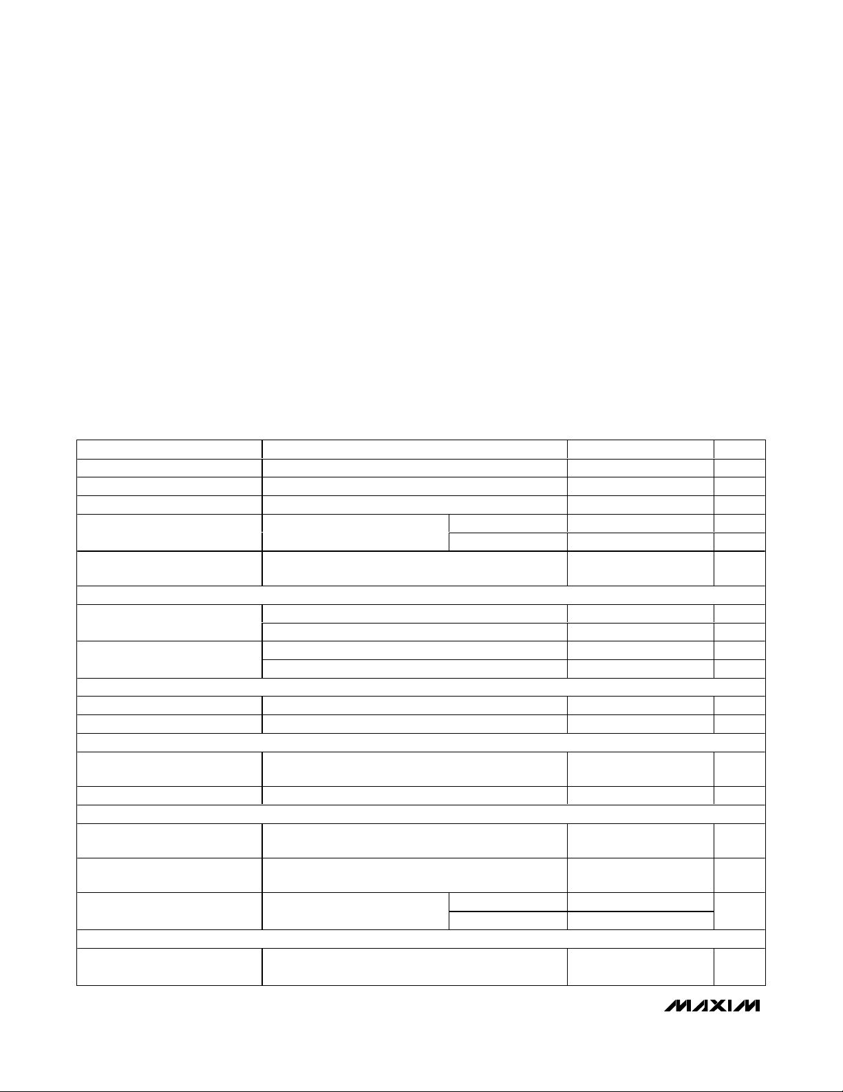
Typical Operating Characteristics
(V
IN12
= V
IN34
= 3.6V, circuit of Figure 4, V
OUT1
= 1.2V, V
OUT2
= 1.8V, V
OUT3
= 2.8V, V
OUT4
= 2.8V, TA = +25°C, unless otherwise noted.)
OUT1 EFFICIENCY vs. LOAD CURRENT
(V
OUT1
= 1.2V)
MAX8667/88 toc01
LOAD CURRENT (mA)
EFFICIENCY (%)
101
10
20
30
40
50
60
70
80
90
0
0.1 1000100
ONLY OUT1 ENABLED
OUT2 EFFICIENCY vs. LOAD CURRENT
(V
OUT2
= 1.8V)
MAX8667/88 toc02
LOAD CURRENT (mA)
EFFICIENCY (%)
1000100101
10
20
30
40
50
60
70
80
90
0
0.1 10000
ONLY OUT2 ENABLED
0.80
0.90
0.85
1.05
1.00
0.95
1.20
1.15
1.10
1.25
0 200100 300 400 500 600
OUT1 LOAD REGULATION
MAX8667/88 toc03
LOAD CURRENT (mA)
OUTPUT VOLTAGE (V)
1.20
1.40
1.30
1.60
1.50
1.80
1.70
1.90
0 400 600200 800 1000 1200
OUT2 LOAD REGULATION
MAX8667/88 toc04
LOAD CURRENT (mA)
OUTPUT VOLTAGE (V)
1.00
1.05
1.10
1.15
1.20
1.25
1.30
1.35
1.40
2.5 3.53.0 4.0 4.5 5.0 5.5
OUT1 OUTPUT VOLTAGE
vs. INPUT VOLTAGE (600mA LOAD)
MAX8667/88 toc05
INPUT VOLTAGE (V)
OUTPUT VOLTAGE (V)
1.60
1.65
1.70
1.75
1.80
1.85
1.90
1.95
2.00
2.5 3.53.0 4.0 4.5 5.0 5.5
OUT2 OUTPUT VOLTAGE
vs. INPUT VOLTAGE (1200mA LOAD)
MAX8667/88 toc06
INPUT VOLTAGE (V)
OUTPUT VOLTAGE (V)
0
1000
500
2000
1500
3000
2500
3500
0 600 900300 1200 1500 1800
SWITCHING FREQUENCY
vs. LOAD CURRENT
MAX8667/88 toc07
LOAD CURRENT (mA)
SWITCHING FREQUENCY (kHz)
OUT2
OUT1
0
20
40
60
80
100
120
1.5 2.52.0 3.0 3.5 4.0 4.5 5.0 5.5
NO-LOAD SUPPLY CURRENT vs. SUPPLY
VOLTAGE ALL REGULATOR ENABLED
MAX8667/88 toc08
SUPPLY VOLTAGE (V)
SUPPLY CURRENT (μA)
SUPPLY VOLTAGE
RISING
SUPPLY VOLTAGE
FALLING
0
20
40
60
80
100
120
1.5 2.52.0 3.0 3.5 4.0 4.5 5.0 5.5
NO-LOAD SUPPLY CURRENT
vs. SUPPLY VOLTAGE OUT1 AND OUT2 ONLY
MAX8667/88 toc09
SUPPLY VOLTAGE (V)
SUPPLY CURRENT (μA)
SUPPLY VOLTAGE
RISING
SUPPLY VOLTAGE
FALLING
Page 5
MAX8667/MAX8668
1.5MHz Dual Step-Down DC-DC Converters
with Dual LDOs and Individual Enables
_______________________________________________________________________________________
5
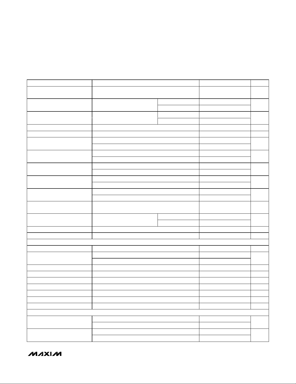
Typical Operating Characteristics (continued)
(V
IN12
= V
IN34
= 3.6V, circuit of Figure 4, V
OUT1
= 1.2V, V
OUT2
= 1.8V, V
OUT3
= 2.8V, V
OUT4
= 2.8V, TA = +25°C, unless otherwise noted.)
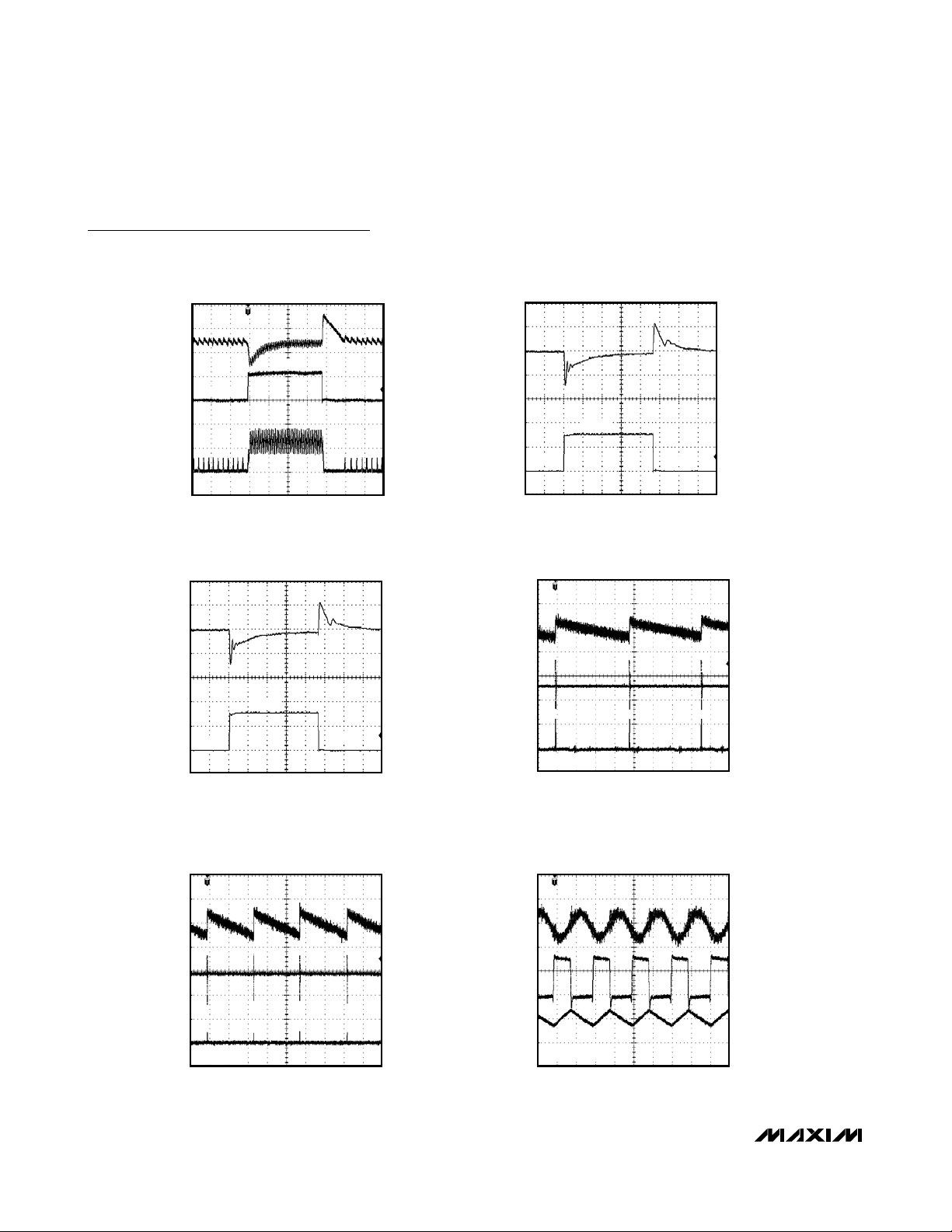
10μs/div
OUT1 LOAD TRANSIENT
V
OUT1
I
OUT1
100mV/div
(AC-COUPLED)
200mA/div
200mA/div
MAX8667/88 toc16
I
L1
300mA
10mA
10mA
NO-LOAD SUPPLY CURRENT vs. SUPPLY
VOLTAGE OUT3 AND OUT4 ONLY
120
100
80
(μA)
IN34
I
V
VOLTAGE
IN34
60
FALLING
40
V
VOLTAGE
20
0
012345
IN34
RISING
SUPPLY VOLTAGE (V)
SUPPLY CURRENT vs. SUPPLY VOLTAGE
1000
900
800
700
600
500
400
300
SUPPLY CURRENT (mA)
200
100
0
2.5 3.53.0 4.0 4.5 5.0 5.5
V
= 5.5V
IN12
SUPPLY VOLTAGE (V)
3.00
2.95
2.90
MAX8667/88 toc10
2.85
2.80
2.75
2.70
OUTPUT VOLTAGE (V)
2.65
2.60
2.55
2.50
IN12 = IN34
2.4Ω LOAD ON OUT1
3.6Ω LOAD ON OUT2
NO LOAD ON OUT3
NO LOAD ON OUT4
OUT3 OUTPUT VOLTAGE
vs. INPUT VOLTAGE (300mA LOAD)
2.5 3.53.0 4.0 4.5 5.0 5.5
INPUT VOLTAGE (V)
EN1/EN2/
I
IN12
EN3/EN4
V
OUT1
V
OUT2
V
OUT3
V
OUT4
+ I
IN34
I
L1
I
L2
MAX8667/88 toc13
OUT3 DROPOUT VOLTAGE
vs. LOAD CURRENT
80
70
MAX8667/88 toc11
60
50
40
30
DROPOUT VOLTAGE (mV)
20
10
0
0 100 200 300
LOAD CURRENT (mA)
ENABLE WAVEFORMS
40
μs/div
MAX8667/88 toc14
5V/div
2V/div
2V/div
2V/div
2V/div
2A/div
2A/div
2A/div
MAX8667/88 toc12
SHUTDOWN WAVEFORMS
EN1/EN2/
EN3/EN4
V
OUT1
V
OUT2
V
OUT3
V
OUT4
40μs/div
MAX8667/88 toc15
5V/div
1V/div
1V/div
1V/div
1V/div
Page 6
MAX8667/MAX8668
1.5MHz Dual Step-Down DC-DC Converters
with Dual LDOs and Individual Enables
6 _______________________________________________________________________________________
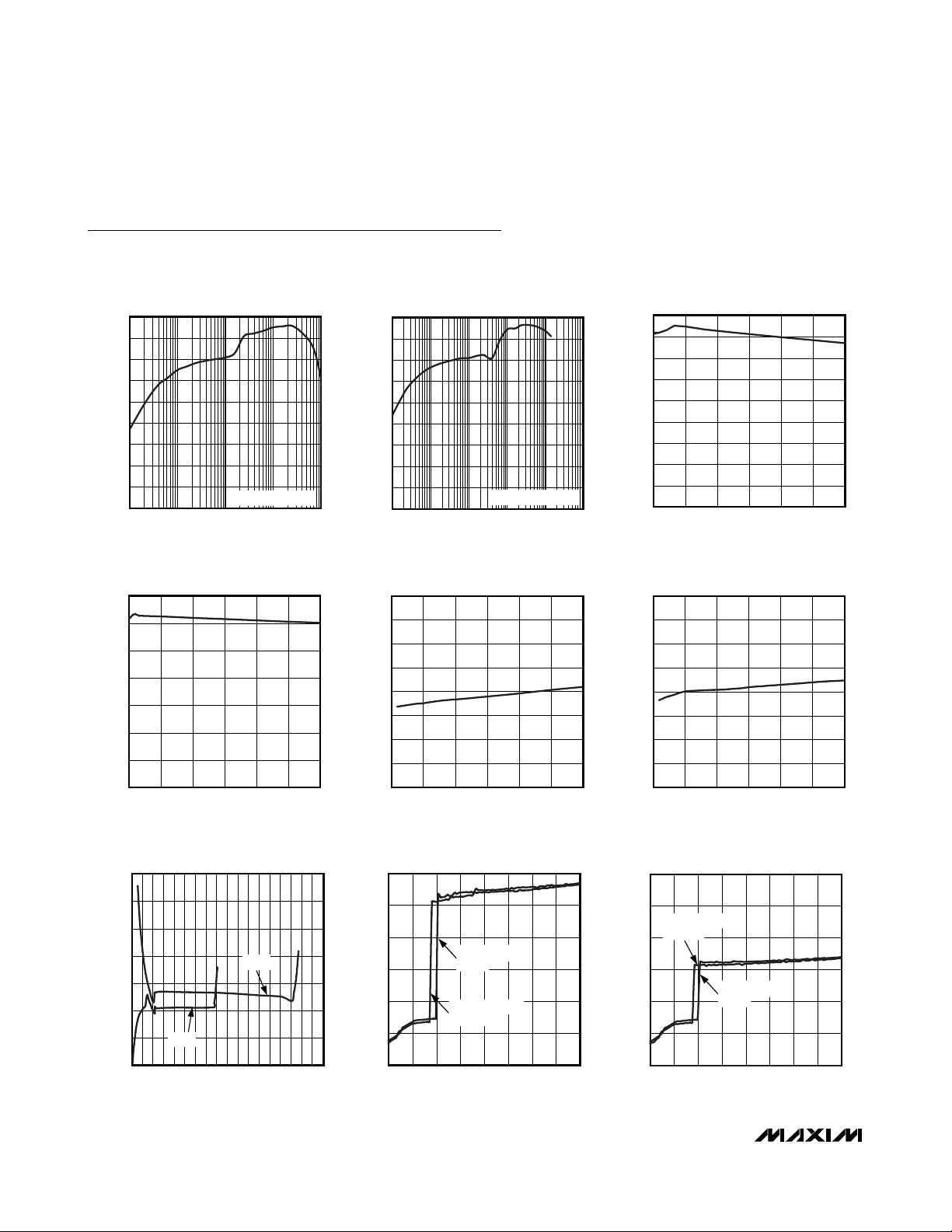
Typical Operating Characteristics (continued)
(V
IN12
= V
IN34
= 3.6V, circuit of Figure 4, V
OUT1
= 1.2V, V
OUT2
= 1.8V, V
OUT3
= 2.8V, V
OUT4
= 2.8V, TA = +25°C, unless otherwise noted.)
OUT2 LOAD TRANSIENT
MAX8667/88 toc17
OUT3 LOAD TRANSIENT
MAX8667/88 toc18
V
OUT2
600mA
I
OUT2
I
L2
10μs/div
10mA10mA
V
OUT4
I
OUT4
OUT4 LOAD TRANSIENT
300mA
0mA
10μs/div
MAX8667/88 toc19
0mA
200mV/div
(AC-COUPLED)
500mA/div
500mA/div
50mV/div
(AC-COUPLED)
200mA/div
V
I
OUT3
OUT3
V
300mA
0mA
OUT1 LIGHT-LOAD SWITCHING
WAVEFORMS
OUT1
V
LX1
I
L1
500μA LOAD
10μs/div
10μs/div
0mA
MAX8667/88 toc20
50mV/div
(AC-COUPLED)
200mA/div
20mV/div
2V/div
100mA/div
V
OUT2 LIGHT-LOAD SWITCHING
WAVEFORMS
OUT2
V
LX2
I
L2
500μA LOAD
40μs/div
MAX8667/88 toc21
20mV/div
2V/div
500mA/div
V
OUT1 HEAVY-LOAD SWITCHING
WAVEFORMS
OUT1
V
LX1
I
L1
500μA LOAD
MAX8667/88 toc22
400ns/div
20mV/div
2V/div
500mA/div
Page 7

MAX8667/MAX8668
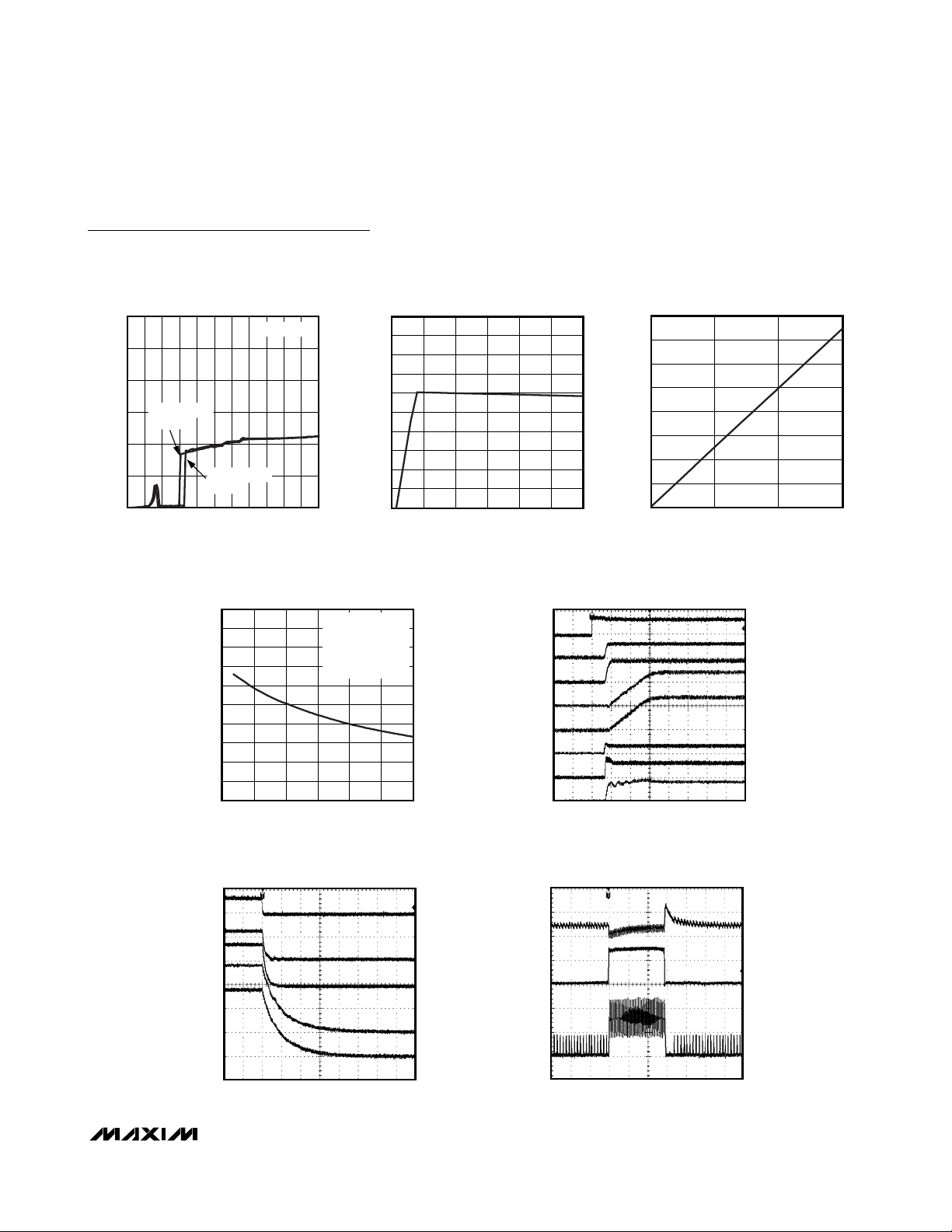
Typical Operating Characteristics (continued)
(V
IN12
= V
IN34
= 3.6V, circuit of Figure 4, V
OUT1
= 1.2V, V
OUT2
= 1.8V, V
OUT3
= 2.8V, V
OUT4
= 2.8V, TA = +25°C, unless otherwise noted.)
1.5MHz Dual Step-Down DC-DC Converters
with Dual LDOs and Individual Enables
_______________________________________________________________________________________
7
V
OUT2
V
LX2
I
L2
OUT2 HEAVY-LOAD SWITCHING
WAVEFORMS
500mA LOAD
400ns/div
OUT3 NOISE
MAX8667/88 toc23
MAX8667/88 toc25
20mV/div
2V/div
500mA/div
100μV/div
PSRR (dB)
POWER-SUPPLY REJECTION RATIO
vs. FREQUENCY
70
60
50
40
30
20
10
0
0.01 10.1 10 100 1000
FREQUENCY (kHz)
OUT4 NOISE
V
I
LOAD
C
OUT3
OUT3
= 2.80V
= 100Ω
= 4.7μF
MAX8667/88 toc26
MAX8667/88 toc24
100μV/div
V
1ms/div
I
OUT3
LOAD
= 2.80V
= 100Ω
1ms/div
V
I
LOAD
OUT4
= 3.30V
= 100Ω
Page 8

MAX8667/MAX8668
1.5MHz Dual Step-Down DC-DC Converters
with Dual LDOs and Individual Enables
8 _______________________________________________________________________________________
Pin Description
PIN
MAX8667 MAX8668
1 EN3 EN3
2 OUT3 OUT3
3 IN34 IN34
4 OUT4 OUT4
5 EN4 EN4
6 GND GND Ground
7 REF REF Reference Output. Bypass REF with a 0.01µF ceramic capacitor to GND.
8 OUT2 — Feedback Input for Regulator 2. Connect OUT2 directly to the output of step-down regulator 2.
9 PGND2 PGND2 Power Ground for Step-Down Regulator 2
10 LX2 LX2 Inductor Connection for Regulator 2
11 IN12 IN12
12 LX1 LX1 Inductor Connection for Regulator 1
13 PGND1 PGND1 Power Ground for Step-Down Regulator 1
14 OUT1 — Feed b ack Inp ut for Reg ul ator 1. C onnect OU T1 d i r ectl y to the outp ut of step - d ow n r eg ul ator 1.
15 EN1 EN1
16 EN2 EN2
— EP EP Exposed Paddle. Connect to GND, PGND1, PGND2, and circuit ground.
NAME
— FB2
— FB1
Enable Input for Regulator 3. Drive EN3 high or connect to IN34 to turn on regulator 3. Drive low
to turn off regulator 3 and reduce input quiescent current.
Output of Regulator 3. Bypass OUT3 with a 4.7µF ceramic capacitor to GND. OUT3 is
discharged to GND through an internal 1kΩ in shutdown.
Input Voltage for LDO Regulators 3 and 4. Supply voltage range is from 1.7V to 5.5V. This
supply voltage must not exceed V
to ground.
Output of Regulator 4. Bypass OUT4 with a 4.7µF ceramic capacitor to GND. OUT4 is
discharged to GND through an internal 1kΩ in shutdown.
Enable Input for Regulator 4. Drive EN4 high or connect to IN34 to turn on regulator 4. Drive low
to turn off regulator 4 and reduce input quiescent current.
Feedback Input for Regulator 2. Connect FB2 to the center of a resistor feedback divider
between the output of regulator 2 and ground to set the output voltage. See the Setting the
Output Voltages and Voltage Positioning section.
Input Voltage for Step-Down Regulators 1 and 2. Supply voltage range is from 2.6V to 5.5V. This
supply voltage must not be less than V
IN12 to ground.
Feedback Input for Regulator 1. Connect FB1 to the center of a resistor feedback divider
between the output of regulator 1 and ground to set the output voltage. See the Setting the
Output Voltages and Voltage Positioning section.
E nab l e Inp ut for Reg ul ator 1. D r i ve E N 1 hi g h or connect to IN 12 to tur n on step - d ow n r eg ul ator 1.
D r i ve l ow to tur n off the r eg ul ator and r ed uce i np ut q ui escent cur r ent.
E nab l e Inp ut for Reg ul ator 2. D r i ve E N 2 hi g h or connect to IN 12 to tur n on step - d ow n r eg ul ator 2.
D r i ve l ow to tur n off the r eg ul ator and r ed uce i np ut q ui escent cur r ent.
FUNCTION
. Connect a 4.7µF or larger ceramic capacitor from IN34
IN12
. Connect a 10µF or larger ceramic capacitor from
IN34
Page 9

MAX8667/MAX8668
1.5MHz Dual Step-Down DC-DC Converters
with Dual LDOs and Individual Enables
_______________________________________________________________________________________ 9
Figure 1. Functional Diagram
REF
GND
IN34
1.7V TO 5.5V
UVLO
EN
REF AND BIAS
IN
EN
IN
REF
EN
STEP-DOWN
OUT1
GND
STEP-DOWN
OUT2
GND
IN12
2.8V TO 5.5V
(2.6V TO 5.5V)
LX1
FB
FB
OUT1
(FB1)
PGND1
LX2
OUT2
(FB2)
PGND2
EN1
EN2
EN3
EN4
PWRON LOGIC
AND ENABLES
() ARE FOR THE MAX8668
LDO
IN
EN
OUT3
GND
OUT
OUT3
LDO
OUT4
GND
OUT
OUT4
IN
EN
Page 10

MAX8667/MAX8668
1.5MHz Dual Step-Down DC-DC Converters
with Dual LDOs and Individual Enables
10 ______________________________________________________________________________________
Detailed Description
The MAX8667/MAX8668 dual step-down converters
with dual low-dropout (LDO) linear regulators are
intended to power low-voltage microprocessors or
DSPs in portable devices. They feature high efficiency
with small external component size. The step-down outputs are adjustable from 0.6V to 3.3V (MAX8668) or
factory preset (MAX8667) with guaranteed output current of 600mA for OUT1 and 1200mA for OUT2. The
1.5MHz hysteretic-PWM control scheme allows for tiny
external components and reduces no-load operating
current to 100µA (typ) with all regulators enabled. Dual,
low-quiescent-current, low-noise LDOs operate down to
1.7V supply voltage. The MAX8667/MAX8668 have
individual enable inputs for each output to facilitate any
supply sequencing.
Step-Down DC-DC Regulators
(OUT1, OUT2)
Step-Down Regulator Architecture
The MAX8667/MAX8668 step-down regulators are optimized for high-efficiency voltage conversion over a
wide load range, while maintaining excellent transient
response, minimizing external component size, and
minimizing output voltage ripple. The DC-DC converters (OUT1, OUT2) also feature an optimized on-resistance internal MOSFET switch and synchronous
rectifier to maximize efficiency. The MAX8667/
MAX8668 utilize a proprietary hysteretic-PWM control
scheme that switches with nearly fixed frequency at up
to 1.5MHz allowing for ultra-small external components.
The step-down converter output current is guaranteed
up to 600mA for OUT1 and 1200mA for OUT2.
When the step-down converter output voltage falls below
the regulation threshold, the error comparator begins a
switching cycle by turning the high-side p-channel
MOSFET switch on. This switch remains on until the minimum on-time (t
ON
) expires and the output voltage is in
regulation or the current-limit threshold (I
LIMP_
) is
exceeded. Once off, the high-side switch remains off
until the minimum off-time (t
OFF
) expires and the output
voltage again falls below the regulation threshold.
During this off period, the low-side synchronous rectifier turns on and remains on until either the high-side
switch turns on or the inductor current reduces to the
rectifier-off current threshold (I
LXOFF
= 60mA typ). The
internal synchronous rectifier eliminates the need for an
external Schottky diode.
Input Supply and Undervoltage Lockout
The input voltage range of step-down regulators OUT1
and OUT2 is 2.6V to 5.5V. This supply voltage must be
greater than or equal to the LDO supply voltage (V
IN34
).
A UVLO circuit prevents step-down regulators OUT1
and OUT2 from switching when the supply voltage is
too low to guarantee proper operation. When V
IN12
falls
below 2.4V (typ), OUT1 and OUT2 are shut down.
OUT1 and OUT2 turn on and begin soft-start when
V
IN12
rises above 2.5V (typ).
Soft-Start
When initially powered up, or enabled with EN_, the
step-down regulators soft-start by gradually ramping
up the output voltage. This reduces inrush current during startup. See the startup waveforms in the
Typical
Operating Characteristics
section.
Current Limit
The MAX8667/MAX8668 limit the peak inductor current
of the p-channel MOSFET (I
LIMP_
). A valley current limit
is used to protect the step-down regulators during
severe overload and output short-circuit conditions.
When the peak current limit is reached, the internal
p-channel MOSFET turns off and remains off until the
output drops below regulation, the inductor current falls
below the valley current-limit threshold, and the minimum off-time has expired.
Voltage Positioning
The OUT1 and OUT2 output voltages and voltage positioning of the MAX8668 are set by a resistor network
connected to FB_. With this configuration, a portion of
the feedback signal is sensed on the switched side of
the inductor, and the output voltage droops slightly as
the load current is increased due to the DC resistance
of the inductor. This output voltage droop is known as
voltage positioning. Voltage positioning allows the load
regulation to be set to match the voltage droop during
a load transient, reducing the peak-to-peak output voltage deviation during a load transient, and reducing the
output capacitance requirements.
Dropout
As the input voltage approaches the output voltage, the
duty cycle of the p-channel MOSFET reaches 100%. In
this state, the p-channel MOSFET is turned on constantly (not switching), and the dropout voltage is the
voltage drop due to the output current across the onresistance of the internal p-channel MOSFET (R
PCH
)
and the inductor’s DC resistance (R
L
):
LDO Linear Regulators (OUT3, OUT4)
The MAX8667/MAX8668 contain two low-dropout linear
regulators (LDOs), OUT3 and OUT4. The LDO output
voltages are factory preset, and each LDO supplies
VI R R
=+
DO LOAD PCH L
()
Page 11

MAX8667/MAX8668
1.5MHz Dual Step-Down DC-DC Converters
with Dual LDOs and Individual Enables
______________________________________________________________________________________ 11
loads up to 300mA. The LDOs include an internal reference, error amplifier, p-channel pass transistor, and
internal voltage-dividers. Each error amplifier compares
the reference voltage to the output voltage (divided by
the internal voltage-divider) and amplifies the difference. If the divided feedback voltage is lower than the
reference voltage, the pass-transistor gate is pulled
lower, allowing more current to pass to the outputs and
increasing the output voltage. If the divided feedback
voltage is too high, the pass-transistor gate is pulled
up, allowing less current to pass to the output.
Input Supply and Undervoltage Lockout
The input voltage range of LDO regulators OUT3 and
OUT4 is 1.7V to 5.5V. This supply voltage must be less
than or equal to the voltage applied to IN12 (V
IN34
≤
V
IN12
).
An undervoltage lockout circuit turns off the LDO regulators when the input supply voltage is too low to guarantee
proper operation. When V
IN34
falls below 1.5V (typ),
OUT3 and OUT4 are shut down. OUT3 and OUT4 turn
on and begin soft-start when V
IN34
rises above 1.6V (typ).
Soft-Start
When initially powered up, or enabled with EN_, the
LDOs soft-start by gradually ramping up the output
voltage. This reduces inrush current during startup. The
soft-start ramp time is typically 100µs from the start of
the soft-start ramp to the output reaching its nominal
regulation voltage.
Current Limit
The OUT3 and OUT4 output current is limited to 375mA
(min). If the output current exceeds the current limit, the
corresponding LDO output voltage drops.
Dropout
The maximum dropout voltage for the linear regulators
is 250mV at 300mA load. To avoid dropout, make sure
the IN34 supply voltage is at least 250mV higher than
the highest LDO output voltage.
Thermal-Overload Protection
Thermal-overload protection limits the total power dissipation in the MAX8667/MAX8668. Thermal-protection
circuits monitor the die temperature. If the die temperature exceeds +160°C, the IC is shut down, allowing the
IC to cool. Once the IC has cooled by 15°C, the IC is
enabled again. This results in a pulsed output during
continuous thermal-overload conditions. The thermaloverload protection protects the MAX8667/MAX8668 in
the event of fault conditions. For continuous operation,
do not exceed the absolute maximum junction temperature of +150°C. See the
Thermal Considerations
sec-
tion for more information.
Figure 2. Timing Diagram
IN12
ENx
OUTx
ENy
OUTy
t
IS THE PERIOD REQUIRED TO ENABLE FROM SHUTDOWN
PWRON
t
PWRON
tEN IS THE ENABLE TIME FOR SUBSEQUENT ENABLE
SIGNALS FOLLOWING THE FIRST ENABLE
t
EN
ENx, ENy ARE ANY COMBINATION OF EN1–EN4.
Page 12

MAX8667/MAX8668
1.5MHz Dual Step-Down DC-DC Converters
with Dual LDOs and Individual Enables
12 ______________________________________________________________________________________
Figure 3. MAX8667 Typical Application Circuit
Figure 4. MAX8668 Typical Application Circuit
C3
INPUT
2.8V TO 5.5V
10μF
0.01μF
C2
C1
EN1
EN2
REF
GND
IN12
IN34
1.7V TO 5.5V
EN3
EN4
OUT3
OUT4
4.7μF
4.7μF
300mA
300mA
C8
C9
4.7μF
MAX8667
OUT2
1.2A
2.2μF
L2
2.2μH
C7
LX2
OUT2
PGND2 PGND1
LX1
OUT1
L1
2.2μH
OUT1
600mA
C6
2.2μF
INPUT
2.6V TO 5.5V
OUT2
0.6V TO 3.3V, 1.2A
C7
2.2μF
10μF
0.01μF
C5
C2
C1
C10*
L2
2.2μH
R5*
IN34
IN12
EN1
EN2
REF
GND
MAX8668
LX2
R3
FB2
R4
PGND1 PGND2
*C10, R5, AND R6 ARE OPTIONAL
EN3
EN4
OUT3
OUT4
LX1
FB1
4.7μF
R1
R2
C8
L1
2.2μH
R6*
C4
OUT3, 300mA
OUT4, 300mA
C9
4.7μF
OUT1
0.6V TO 3.3V, 600mA
C6
2.2μF
Page 13

MAX8667/MAX8668
1.5MHz Dual Step-Down DC-DC Converters
with Dual LDOs and Individual Enables
______________________________________________________________________________________ 13
Applications Information
Setting the Output Voltages
and Voltage Positioning
The LDO output voltages of the MAX8667/MAX8668,
and the step-down outputs of the MAX8667 are factory
preset. See the
Selector Guide
to find the part number
corresponding to the desired output voltages.
The OUT1 and OUT2 output voltages of the MAX8668
are set by a resistor network connected to FB_ as
shown in Figure 5. With this configuration, a portion of
the feedback signal is sensed on the switched side of
the inductor (LX), and the output voltage droops slightly
as the load current is increased due to the DC resistance of the inductor (DCR). This allows the load regulation to be set to match the voltage droop during a
load transient (voltage positioning), reducing the peakto-peak output-voltage deviation during a load transient, and reducing the output capacitance
requirements.
For the simplest method of setting the output voltage,
R6 is not installed. Choose the value of R2 (a good
starting value is 100kΩ), and then calculate the value of
R1 as follows:
where VFBis the feedback regulation voltage (0.6V).
With the voltage set in this manner, the voltage positioning depends only on the DCR, and the maximum
output voltage droop is:
Setting the Output Voltages with
Reduced Voltage Positioning
To obtain less voltage positioning than described in the
previous section, use the following procedure for setting the output voltages. The OUT1 and OUT2 output
voltages and voltage positioning of the MAX8668 are
set by a resistor network connected to FB_ as shown in
Figure 5.
To set the output voltage (V
OUT
), first select a value for
R2 (a good starting value is 100kΩ). Then calculate the
value of REQ(the equivalent parallel resistance of R1
and R6) as follows:
where VFBis the feedback-regulation voltage (0.6V).
Calculate the factor m based on the desired load-regulation improvement:
where I
OUT(MAX)
is the maximum output current, DCR is
the inductor series resistance, and ΔV
OUT(DESIRED)
is the
maximum allowable droop in the output voltage at full
load. The calculated value for m must be between 1.1 and
2; m = 2 results in a 2x improvement in load regulation.
Now calculate the values of R1 and R6 as follows:
The value of R1 should always be lower than the value
of R6.
Power-Supply Sequencing
The MAX8667/MAX8668 have individual enable inputs
for each regulator to allow complete control over the
power sequencing. When all EN_ inputs are low, the IC
is in low-power shutdown mode, reducing the supply
current to less than 1µA. After one of the EN_ inputs
asserts high, the corresponding regulator begins softstart after a delay of tEN(see Figure 2). The first output
enabled from shutdown mode or initially powering up
the IC has a longer delay (t
PWRON
) as the IC exits the
low-power shutdown mode.
Inductor Selection
The MAX8667/MAX8668 step-down converters operate
with inductors between 2.2µH and 4.7µH. Low inductance values are physically smaller, but require faster
switching, resulting in some efficiency loss. The inductor’s DC current rating must be high enough to account
Figure 5. MAX8668 Feedback Network
RR
12 1=× −
ΔV DCR I
OUT MAX OUT MAX() ()
V
⎛
OUT
⎜
⎝
V
FB
⎞
⎟
⎠
=×
R1
R2
L1 DCR
C4
(OPTIONAL)
OUT
R6
ESR
C6
R
LOAD
LX_
FB_
I DCR
OUT MAX
m
=
V
Δ
OUT DESIRED
×
()
()
RR m
1
=×
EQ
RR
6
=×
EQ
m
m
1
−
R
V
⎛
OUT
=−
EQ
⎜
⎝
V
FB
⎞
×12
R
⎟
⎠
Page 14

MAX8667/MAX8668
1.5MHz Dual Step-Down DC-DC Converters
with Dual LDOs and Individual Enables
14 ______________________________________________________________________________________
for peak ripple current and load transients. The stepdown converter’s unique architecture has minimal current overshoot during startup and load transients and in
most cases, an inductor capable of 1.3x the maximum
load current is acceptable.
For output voltages above 2V, when light-load efficiency
is important, the minimum recommended inductor is
2.2µH. For optimum voltage-positioning load transients,
choose an inductor with DC series resistance in the
50mΩ to 150mΩ range. For higher efficiency at heavy
loads (above 200mA) and minimal load regulation,
keep the inductor resistance as small as possible. For
light-load applications (up to 200mA), higher resistance
is acceptable with very little impact on performance.
Capacitor Selection
Input Capacitors
The input capacitor for the step-down converters (C2 in
Figures 3 and 4) reduces the current peaks drawn from
the battery or input power source and reduces switching noise in the IC. The impedance of C2 at the switching frequency should be very low. Surface-mount
ceramic capacitors are a good choice due to their
small size and low ESR. Make sure the capacitor maintains its capacitance over temperature and DC bias.
Ceramic capacitors with X5R or X7R temperature characteristics generally perform well. A 10µF ceramic
capacitor is recommended.
A 4.7µF ceramic capacitor is recommended for the
LDO input capacitor (C3 in Figure 3).
Step-Down Output Capacitors
The step-down output capacitors (C6 and C7 in Figures
3 and 4) are required to keep the output-voltage ripple
small and to ensure regulation loop stability. These
capacitors must have low impedance at the switching
frequency. Surface-mount ceramic capacitors are a
good choice due to their small size and low ESR. Make
sure the capacitor maintains its capacitance over temperature and DC bias. Ceramic capacitors with X5R or
X7R temperature characteristics generally perform well.
The output capacitance can be very low. For most
applications, a 2.2µF ceramic capacitor is sufficient.
For optimum load-transient performance and very low
output ripple, the output capacitor value in µF should
be equal to or greater than the inductor value in µH.
Feed-Forward Capacitor
The feed-forward capacitors on the MAX8668 (C4 and
C5 in Figure 4) set the feedback loop response, control
the switching frequency, and are critical in obtaining
the best efficiency possible. Small X7R and C0G
ceramic capacitors are recommended.
For OUT1, calculate the value of C4 as follows:
C4 = 1.2 x 10⁻⁵(s/V) x (V
OUT
/ R1)
For OUT2, calculate the value of C5 and C10 as follows:
Cff= 1.2 x 10⁻⁵(s/V) x (V
OUT
/ R3)
Cff= C5 + (C10 / 2)
(C10 / C5) + 1 = (V
OUT
/ VFB), where VFBis 0.6V.
Rearranging the formulas:
C10 = 2 x Cffx (V
OUT
- VFB)/(V
OUT
+ VFB)
C5 = Cff– (C10 / 2)
C10 is needed if V
OUT
> 1.5V or V
IN12
can be less than
V
OUT
/ 0.65.
Table 1. Recommended Inductors
MANUFACTURER INDUCTOR L (µH) RL (mΩ) CURRENT RATING (A) L x W x H (mm)
FDK MIPF2016 2.2 110 1.1 2.0 x 1.6 x 1.0
FDK MIPF2520D 2.2 80 1.3 2.5 x 2.0 x 1.0
Murata
Sumida CDRH2D09 2.2 120 0.44 3.2 x 3.2 x 1.0
TDK GLF251812T 2.2 200 0.6 2.5 x 1.8 x 1.35
TOKO D2812C 2.2 140 0.77 2.8 x 2.8 x 1.2
TOKO MDT2520-CR 2.2 80 0.7 2.5 x 2.0 x 1.0
Wurth
Taiyo Yuden CB2518T 2.2 90 0.51 2.5 x 1.8 x 2.0
LQH32CN2R2M5 2.2 97 0.79 3.2 x 2.5 x 1.55
LQM31P 2.2 220 0.9 3.2 x 1.6 x 0.95
TPC Series 2.2 55 1.8 4.0 x 4.0 x 1.1
TPC Series 4.7 124 1.35 4.0 x 4.0 x 1.1
Page 15

MAX8667/MAX8668
1.5MHz Dual Step-Down DC-DC Converters
with Dual LDOs and Individual Enables
______________________________________________________________________________________ 15
LDO Output Capacitor and Stability
Connect a 4.7µF ceramic capacitor between OUT3 and
GND, and a second 4.7µF ceramic capacitor from
OUT4 to GND. For a constant loading above 10mA, the
output capacitors can be reduced to 2.2µF. The equivalent series resistance (ESR) of the LDO output capacitors affects stability and output noise. Use output
capacitors with an ESR of 0.1Ω or less to ensure stable
operation and optimum transient response. Surfacemount ceramic capacitors have very low ESR and are
commonly available. Connect these capacitors as
close as possible to the IC’s pins to minimize PCB trace
inductance.
Thermal Considerations
The maximum package power dissipation of the
MAX8667/MAX8668 is 1667mW. Make sure the power
dissipated by the MAX8667/MAX8668 does not exceed
this rating. The total IC power dissipation is the sum of
the power dissipation of the four regulators:
Estimate the OUT1 and OUT2 power dissipations as
follows:
where RLis the inductor’s DC resistance, and η is the
efficiency (see the
Typical Operating Characteristics
section).
Calculate the OUT3 and OUT4 power dissipations as
follows:
The maximum junction temperature of the MAX8667/
MAX8668 is +150°C. The junction-to-case thermal
resistance (θ
JC
) of the MAX8667/MAX8668 is 6.9°C/W.
When mounted on a single-layer PCB, the junction to
ambient thermal resistance (θ
JA
) is about 64°C/W.
Mounted on a multilayer PCB, θJAis about 48°C/W.
Calculate the junction temperature of the
MAX8667/MAX8668 as follows:
where TAis the maximum ambient temperature. Make
sure the calculated value of TJdoes not exceed the
+150°C maximum.
PCB Layout
High switching frequencies and relatively large peak
currents make PCB layout a very important aspect of
design. Good design minimizes excessive EMI on the
feedback paths and voltage gradients in the ground
plane, both of which can result in instability or regulation errors. Connect the input capacitors as close as
possible to the IN_ and PGND_ pins. Connect the
inductor and output capacitors as close as possible to
the IC and keep the traces short, direct, and wide.
The feedback network traces are sensitive to inductor
magnetic field interference. Route these traces away
from the inductors and noisy traces such as LX. Keep
the feedback components close to the FB_ pin.
Connect GND and PGND_ to the ground plane.
Connect the exposed paddle to the ground plane with
one or more vias to help conduct heat away from the
IC.
Refer to the MAX8668 evaluation kit for a PCB layout
example.
PPPPP
=+++
DDDDD
1234
=× ×
PI V
D OUT OUT 11 1
=× ×
PI V
D OUT OUT 22 2
PI V V
=× −
D OUT IN OUT 3334 3
()
1
1
−η
η
−η
η
TTP
=+× θ
JADJA
PI V V
=×−
D OUT IN OUT 4434 4
()
Page 16

MAX8667/MAX8668
1.5MHz Dual Step-Down DC-DC Converters
with Dual LDOs and Individual Enables
16 ______________________________________________________________________________________
Chip Information
PROCESS: BiCMOS
Ordering Information (continued)
All MAX8667/MAX8668 parts are in a 16-pin, thin QFN, 3mm x
3mm package and operate in the -40°C to = +85°C extended
temperature range.
+
Denotes a lead-free package.
PART PKG CODE TOP MARK
T1633-4 AFJ
T1633-4 AFQ
T1633-4 AER
T1633-4 AFK
T1633-4 AFR
MAX8668ETET+ T1633-4 AFS
T1633-4 AFL
T1633-4 AFT
T1633-4 AFU
T1633-4 AFV
Selector Guide
PART
OUT1
(V)
OUT2
(V)
OUT3
(V)
OUT4
(V)
1.20 1.80 2.80 2.80
1.20 1.80 2.85 2.85
1.20 1.80 1.20 1.20
1.60 1.80 2.80 1.20
1.80 1.20 2.60 2.80
1.30 1.30 3.30 2.70
MAX8668ETEA+ ADJ ADJ 2.80 2.80
MAX8668ETEP+ ADJ ADJ 3.30 1.80
ADJ ADJ 2.80 1.20
MAX8668ETET+ ADJ ADJ 3.30 3.30
MAX8668ETEU+ ADJ ADJ 3.30 2.80
MAX8668ETEV+ ADJ ADJ 3.30 2.50
ADJ ADJ 3.30 3.00
MAX8668ETEX+ ADJ ADJ 2.80 1.80
MAX8667ETEHR+
MAX8667ETEJS+
MAX8668ETEA+
MAX8668ETEP+
MAX8668ETEQ+
MAX8668ETEU+
MAX8668ETEV+
MAX8668ETEW+
MAX8668ETEX+
MAX8667ETEAA+
MAX8667ETEAB+
MAX8667ETEAC+
MAX8667ETECQ+
MAX8667ETEHR+
MAX8667ETEJS+
MAX8668ETEQ+
MAX8668ETEW+
Page 17

MAX8667/MAX8668
1.5MHz Dual Step-Down DC-DC Converters
with Dual LDOs and Individual Enables
______________________________________________________________________________________ 17
Package Information
(The package drawing(s) in this data sheet may not reflect the most current specifications. For the latest package outline information
go to www.maxim-ic.com/packages
.)
MARKING
D/2
D
E
E/2
AAAA
C
L
0.10 C 0.08 C
A
A2
A1
(NE - 1) X e
(ND - 1) X e
C
L
L
e
k
L
C
L
e
E2/2
E2
D2/2
D2
b
0.10 M C A B
C
L
L
e
12x16L QFN THIN.EPS
PACKAGE OUTLINE
8, 12, 16L THIN QFN, 3x3x0.8mm
21-0136
1
I
2
Page 18

MAX8667/MAX8668
1.5MHz Dual Step-Down DC-DC Converters
with Dual LDOs and Individual Enables
Maxim cannot assume responsibility for use of any circuitry other than circuitry entirely embodied in a Maxim product. No circuit patent licenses are
implied. Maxim reserves the right to change the circuitry and specifications without notice at any time.
18
____________________Maxim Integrated Products, 120 San Gabriel Drive, Sunnyvale, CA 94086 408-737-7600
© 2007 Maxim Integrated Products is a registered trademark of Maxim Integrated Products. Inc.
Package Information (continued)
(The package drawing(s) in this data sheet may not reflect the most current specifications. For the latest package outline information
go to www.maxim-ic.com/packages
.)
8L 3x3
PKG
REF. MIN.
MIN.
NOM. M
3.00 3.10
0.65 BSC.
0.55 0.75
8
2
2
0.02
0.20 REF
-
AX.
0.05
-
0.70 0.75 0.80
A
b
0.25 0.30 0.35
2.90
D
2.90 3.00 3.10
E
e
0.35
L
ND
NE
A1
A2
k
0.25
0
12L 3x3
NOM. MAX. NOM.
0.70
0.75
0.50 BSC.
0
0.20 REF
0.25
3.00
3.00
0.55
0.02
0.80
0.30
3.10
3.10
0.65
12N
3
3
0.05
-
-
0.20
2.90
2.90
0.45
0.25
16L 3x3
MIN. MAX.
0.70
0.75
0.25
3.00
3.00
0.50 BSC.
0.40
040.02
0.20 REF
0.80
0.30
3.10
3.10
0.50
16
4
0.05
-
0.20
2.90
2.90
0.30
0.25
EXPOSED PAD VARIATIONS
PKG.
CODES
TQ833-1 1.250.25 0.70 0.35 x 45° WEE C1.250.700.25
T1233-1
3
T1233-
T1233-4
T1633-2 0.9 5
T1633F-3
T1633FH-3 0.65 0.80 0.95
T1633-4 0.9 5
-
T1633-5 0.9 5
D2
MIN.
0.95
0.95
0.95
0.65
MAX.
NOM.
1.25
1.10
1.25
1.10
1.251.10
1.25
1.10
0.95
0.80
1.10 1.25 0.95 1.10
1.25
1.10
E2
NOM.
MIN.
0.95
0.95 1.10 0.35 x 45°1.25 WEED-1
0.95
0.65
0.65 0.80
1.10
1.100.95
1.10
0.80
1.10
MAX.
1.25
1.25
0.95
0.95
1.25
1.25
ID
PIN
0.35 x 45°
0.35 x 45°
0.35 x 45°
0.225 x 45°
0.225 x 45°
0.35 x 45°
0.35 x 45°
JEDEC
WEED-1
WEED-11.25
WEED-2
WEED-2
WEED-2
WEED-2
WEED-20.95
NOTES:
1. DIMENSIONING & TOLERANCING CONFORM TO ASME Y14.5M-1994.
2. ALL DIMENSIONS ARE IN MILLIMETERS. ANGLES ARE IN DEGREES.
3. N IS THE TOTAL NUMBER OF TERMINALS.
4. THE TERMINAL #1 IDENTIFIER AND TERMINAL NUMBERING CONVENTION SHALL CONFORM TO
JESD 95-1 SPP-012. DETAILS OF TERMINAL #1 IDENTIFIER ARE OPTIONAL, BUT MUST BE LOCATED
WITHIN THE ZONE INDICATED. THE TERMINAL #1 IDENTIFIER MAY BE EITHER A MOLD OR
MARKED FEATURE.
5. DIMENSION b APPLIES TO METALLIZED TERMINAL AND IS MEASURED BETWEEN 0.20 mm AND 0.25 mm
FROM TERMINAL TIP.
6. ND AND NE REFER TO THE NUMBER OF TERMINALS ON EACH D AND E SIDE RESPECTIVELY.
7. DEPOPULATION IS POSSIBLE IN A SYMMETRICAL FASHION.
8. COPLANARITY APPLIES TO THE EXPOSED HEAT SINK SLUG AS WELL AS THE TERMINALS.
9. DRAWING CONFORMS TO JEDEC MO220 REVISION C.
10. MARKING IS FOR PACKAGE ORIENTATION REFERENCE ONLY.
11. NUMBER OF LEADS SHOWN ARE FOR REFERENCE ONLY.
12. WARPAGE NOT TO EXCEED
0.10mm.
PACKAGE OUTLINE
8, 12, 16L THIN QFN, 3x3x0.8mm
21-0136
I
2
2
 Loading...