

Page 1
_______________General Description
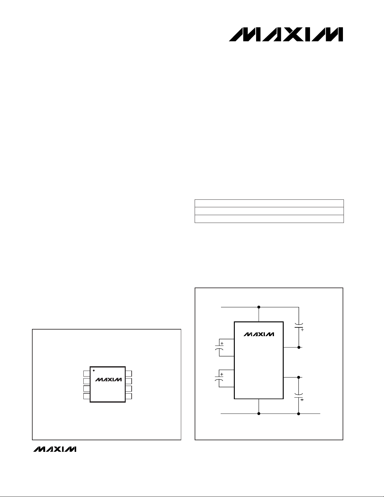
The MAX865 is a CMOS charge-pump DC-DC converter in an ultra-small µMAX package. It produces positive
and negative outputs from a single positive input, and
requires only four capacitors. The charge pump first
doubles the input voltage, then inverts the doubled voltage. The input voltage ranges from +1.5V to +6.0V.
The internal oscillator is guaranteed to be between
20kHz and 38kHz, keeping noise above the audio
range while consuming minimal supply current. A 75Ω
output impedance permits useful output currents up to
20mA.
The MAX865 comes in a 1.11mm-high, 8-pin µMAX
package that occupies half the board area of a standard 8-pin SOIC. For a device with selectable frequencies and logic-controlled shutdown, refer to the MAX864
data sheet.
________________________Applications
Low-Voltage GaAsFET Bias in Wireless Handsets
VCO and GaAsFET Supplies
Split Supply from 3 Ni Cells or 1 Li+ Cell
Low-Cost Split Supply for Low-Voltage
Data-Acquisition Systems
Split Supply for Analog Circuitry
LCD Panels
____________________________Features
♦ 1.11mm-High µMAX Package
♦ Compact: Circuit Fits in 0.08in
2
♦ Requires Only Four Capacitors
♦ Dual Outputs (positive and negative)
♦ +1.5V to +6.0V Input Voltage
♦ 20kHz (min) Frequency (above the audio range)
MAX865
Compact, Dual-Output Charge Pump
________________________________________________________________
Maxim Integrated Products
1
1
2
3
4
8
7
6
5
C1+
V+
IN
GND
V-
C2-
C2+
C1-
MAX865
µMAX
TOP VIEW
__________________Pin Configuration
MAX865
C1+
V+
GND
GND
+VIN to ±2V
IN
CONVERTER
V-
IN
GND
C1-
C2+
C2-
+2*V
IN
V
IN
(+1.5V to +6.0V)
-2*V
IN
__________Typical Operating Circuit
19-0472; Rev 1; 7/97
PART
MAX865C/D
MAX865EUA -40°C to +85°C
0°C to +70°C
TEMP. RANGE PIN-PACKAGE
Dice
8 µMAX
______________Ordering Information
For free samples & the latest literature: http://www.maxim-ic.com, or phone 1-800-998-8800.
For small orders, phone 408-737-7600 ext. 3468.
Page 2
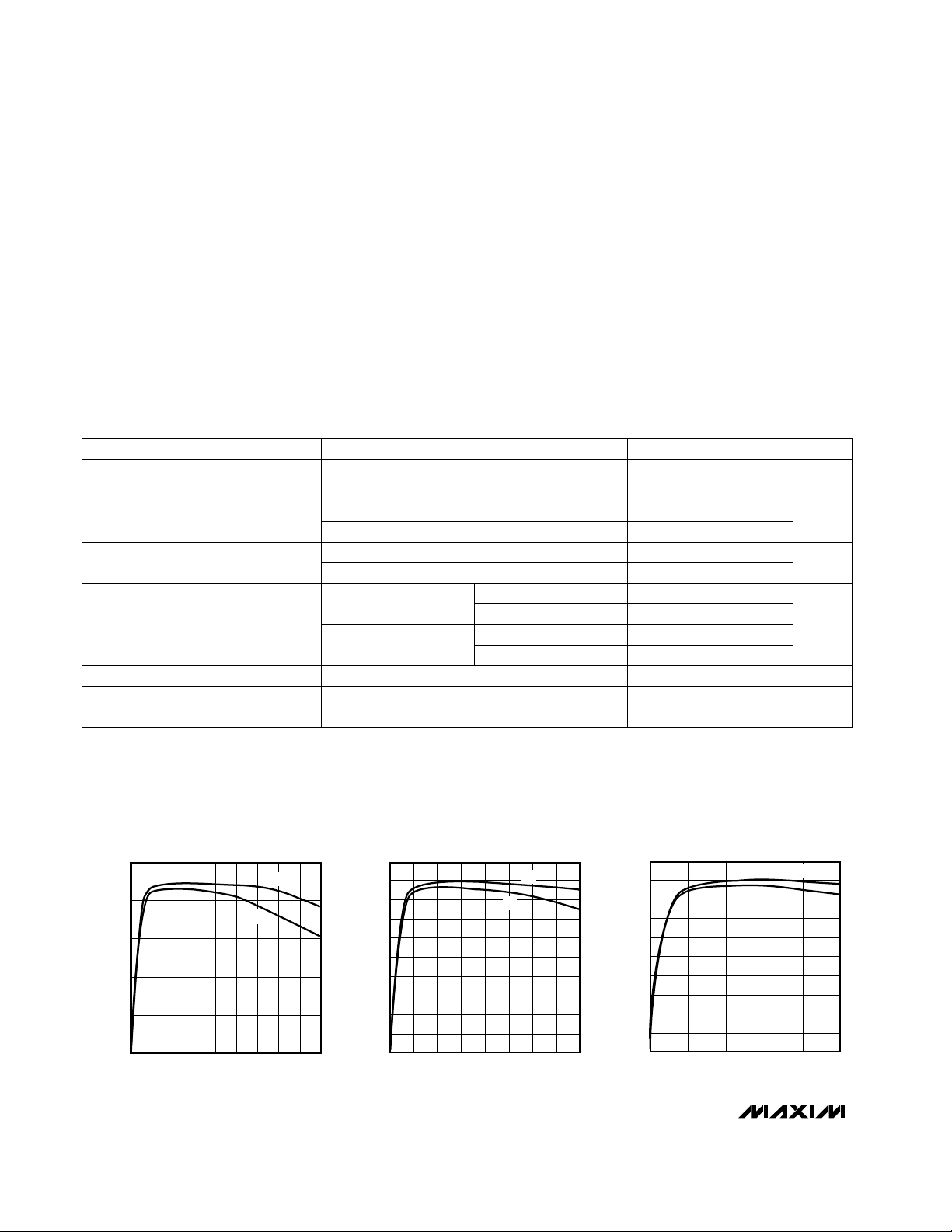
100
90
0
0 2 8 10 18
EFFICIENCY vs. OUTPUT CURRENT
(V
IN
= 5V)
30
20
10
80
70
MAX865-01
OUTPUT CURRENT (mA)
EFFICIENCY (%)
4 6 12 14
50
40
60
16
V-
V+
100
90
0
0 1 3 4 8
EFFICIENCY vs. OUTPUT CURRENT
(V
IN
= 3.3V)
30
20
10
80
70
MAX865-02
OUTPUT CURRENT (mA)
EFFICIENCY (%)
2 5 6
50
40
60
7
V-
V+
100
90
0
0
1.0
2.5
EFFICIENCY vs. OUTPUT CURRENT
(V
IN
= 2V)
30
20
10
80
70
MAX865-03
OUTPUT CURRENT (mA)
EFFICIENCY (%)
0.5 1.5
50
40
60
2.0
V-
V+
__________________________________________Typical Operating Characteristics
(Circuit of Figure 1, VIN= 5V, TA= +25°C, unless otherwise noted.)
MAX865
Compact, Dual-Output Charge Pump
2 _______________________________________________________________________________________
ABSOLUTE MAXIMUM RATINGS
ELECTRICAL CHARACTERISTICS
(VIN= 5V, C1 = C2 = C3 = C4 = 3.3µF, TA= T
MIN
to T
MAX
, unless otherwise noted. Typical values are at TA= +25°C.)
Stresses beyond those listed under “Absolute Maximum Ratings” may cause permanent damage to the device. These are stress ratings only, and functional
operation of the device at these or any other conditions beyond those indicated in the operational sections of the specifications is not implied. Exposure to
absolute maximum rating conditions for extended periods may affect device reliability.
V+ to GND.................................................................+12V, -0.3V
IN to GND.................................................................+6.2V, -0.3V
V- to GND..................................................................-12V, +0.3V
V- Output Current .............................................................100mA
V- Short-Circuit to GND ................................................Indefinite
Continuous Power Dissipation (T
A
= +70°C)
µMAX (derate 4.1mW/°C above +70°C) .......................330mW
Operating Temperature Range
MAX865EUA.....................................................-40°C to +85°C
Storage Temperature Range.............................-65°C to +160°C
Lead Temperature (soldering, 10sec).............................+300°C
T
A
= +25°C
R
LOAD
= 10kΩ
R
LOAD
= 10kΩ
IL= 5mA
V+ = 10V (forced),
IV-= 1mA
IV+= 1mA,
IV-= 0mA
TA= -40°C to +85°C (Note 1)
TA= +25°C
TA= -40°C to +85°C (Note 1)
CONDITIONS
0.6 1.05
V6.0Maximum Supply Voltage
V2.0 1.5Minimum Supply Voltage
%85Power Efficiency
Ω
140
Output Resistance
75 100
280
mA
1.15
Supply Current
19.5 24 32.5
kHz
18 34
Oscillator Frequency
150 200
UNITSMIN TYP MAXPARAMETER
TA= +25°C
TA= T
MIN
to T
MAX
TA= +25°C
TA= T
MIN
to T
MAX
V-, RL= ∞
V+, RL= ∞
%
90 98
Voltage Conversion Efficiency
95 99
Note 1: These specifications are guaranteed by design and are not production tested.
Page 3
MAX865
Compact, Dual-Output Charge Pump
_______________________________________________________________________________________
3
10
8
-10
0 2 6 14
OUTPUT VOLTAGE vs.
OUTPUT CURRENT
-4
-6
-8
6
4
MAX865-04
OUTPUT CURRENT (mA)
OUTPUT VOLTAGE, V+, V- (V)
4 8 10
0
-2
2
12
V-
C1 = C2 = C3 = C4 = 3.3µF
V
IN
= 4.75V
V-
BOTH V+ AND
V- LOADED EQUALLY
V+
V+
400
350
0
0 20 25 50
OUTPUT VOLTAGE RIPPLE
vs. PUMP CAPACITANCE
100
50
300
MAX865-05
PUMP CAPACITANCE (µF)
OUTPUT VOLTAGE RIPPLE (mVp-p)
5 10 15 30 35
200
150
250
40 45
C1 = C2 = C3 = C4
A
B
D
E
F
C
A: V+, IN = 4.75V, V+ + |V-| = 16V
B: V+, IN = 3.15V, V+ + |V-| = 10V
C: V+, IN = 1.90V, V+ + |V-| = 6V
D: V-, IN = 4.75V, V+ + |V-| = 16V
E: V-, IN = 3.15V, V+ + |V-| = 10V
F: V-, IN = 1.90V, V+ + |V-| = 6V
7
6
0
0 20 25 50
OUTPUT CURRENT
vs. PUMP CAPACITANCE
2
1
5
MAX865-06
PUMP CAPACITANCE (µF)
OUTPUT CURRENT, V+ TO V- (mA)
5 10 15 30 35
3
4
40 45
VIN = 4.75V, V+ + |V-| = 16V
C1 = C2 = C3 = C4
VIN = 3.15V, V+ + |V-| = 10V
VIN = 1.90V, V+ + |V-| = 6V
1000
900
0
2.0 3.5 4.0 6.0
SUPPLY CURRENT
vs. SUPPLY VOLTAGE
300
200
100
800
700
MAX865-07
SUPPLY VOLTAGE (V)
SUPPLY CURRENT (µA)
2.5
3.0
4.5
400
600
500
5.0 5.5
C1 = C2 = C3 = C4 = 3.3µF
300
0
-55 5
25
125
OUTPUT RESISTANCE
vs. TEMPERATURE
100
50
250
MAX865-08
TEMPERATURE (°C)
OUTPUT RESISTANCE (Ω)
-35
-15
45
65
200
150
85
105
C1 = C2 = C3 = C4 = 3.3µF
V-, VIN = 3.3V
V+, VIN = 3.3V
V+, VIN = 5.0V
V-, VIN = 5.0V
27
15
-40 0 20 100
PUMP FREQUENCY
vs. TEMPERATURE
19
17
25
MAX865-09
TEMPERATURE (°C)
PUMP FREQUENCY (kHz)
-20 40
23
21
60
80
C1 = C2 = C3 = C4 = 3.3µF
VIN = 5.0V
VIN = 3.3V
VIN = 2.0V
250
0
2.0 3.0 3.5 6.0
OUTPUT RESISTANCE
vs. SUPPLY VOLTAGE
50
200
MAX865-10
SUPPLY VOLTAGE (V)
OUTPUT RESISTANCE (Ω)
2.5 4.0 4.5
150
100
5.0 5.5
C1 = C2 = C3 = C4 = 3.3µF
V-
V+
____________________________Typical Operating Characteristics (continued)
(Circuit of Figure 1, VIN= 5V, TA= +25°C, unless otherwise noted.)
Page 4

_____________________Pin Description
NAME FUNCTION
1
C1-
Negative Terminal of the Flying Boost
Capacitor
2 C2+
Positive Terminal of the Flying
Inverting Capacitor
PIN
3 C2-
Negative Terminal of the Flying
Inverting Capacitor
4 V- Output of the Inverting Charge Pump
8 C1+
Positive Terminal of the Flying Boost
Capacitor
7 V+ Output of the Boost Charge Pump
6 IN Positive Power-Supply Input
5 GND Ground
Figure 1. Test Circuit
MAX865
Compact, Dual-Output Charge Pump
4 _______________________________________________________________________________________
____________________________Typical Operating Characteristics (continued)
(Circuit of Figure 1, VIN= 5V, TA= +25°C, unless otherwise noted.)
10µs/div
V
IN
= 4.75V, 1mA LOAD
OUTPUT RIPPLE
(C1 = C2 = C3 = C4 = 1µF)
V- OUTPUT
20mV/div
V+ OUTPUT
50mV/div
10µs/div
V
IN
= 4.75V, 1mA LOAD
OUTPUT RIPPLE
(C1 = C2 = C3 = C4 = 3.3µF)
V- OUTPUT
10mV/div
V+ OUTPUT
10mV/div
V
IN
3.3µF
C1-
C2+
3.3µF
C2-
V-
MAX865
C1+
V+
IN
GND
3.3µF
3.3µF
OUT+
I
+
V
R
+
L
IV-
R
-
L
OUT-
Page 5

MAX865
Compact, Dual-Output Charge Pump
_______________________________________________________________________________________ 5
_______________Detailed Description
The MAX865 contains all the circuitry needed to implement a voltage doubler/inverter. Only four external
capacitors are needed. These may be polarized electrolytic or ceramic capacitors with values ranging from
1µF to 100µF.
Figure 2a shows the ideal operation of the positive voltage doubler. The on-chip oscillator generates a 50%
duty-cycle clock signal. During the first half cycle,
switches S2 and S4 open, switches S1 and S3 close,
and capacitor C1 charges to the input voltage (VIN).
During the second half cycle, switches S1 and S3
open, switches S2 and S4 close, and capacitor C1 is
level shifted upward by VIN. Assuming ideal switches
and no load on C3, charge transfers into C3 from C1
such that the voltage on C3 will be 2VIN, generating the
positive supply output (V+).
Figure 2b illustrates the ideal operation of the negative
converter. The switches of the negative converter are
out of phase with the positive converter. During the
second half cycle, switches S6 and S8 open and
switches S5 and S7 close, charging C2 from V+
(pumped up to 2VINby the positive charge pump) to
GND. In the first half of the clock cycle, switches S5
and S7 open, switches S6 and S8 close, and the
charge on capacitor C2 transfers to C4, generating the
negative supply. The eight switches are CMOS power
MOSFETs. Switches S1, S2, S4, and S5 are P-channel
devices, while switches S3, S6, S7, and S8 are N-channel devices.
Charge-Pump Output
The MAX865 is not a voltage regulator: the output
source resistance of either charge pump is approximately 150Ω at room temperature with VIN= +5V, and
V+ and V- will approach +10V and -10V, respectively,
when lightly loaded. Both V+ and V- will droop toward
GND as the current draw from either V+ or V- increases, since V- is derived from V+. Treating each converter separately, the droop of the negative supply
(V
DROOP-
) is the product of the current draw from V(IV-) and the source resistance of the negative converter (RS-):
The droop of the positive supply (V
DROOP+
) is the
product of the current draw from the positive supply
(I
LOAD+
) and the source resistance of the positive
IN
a) b)
S1
S3
C1+
C1
C3
C1-
S2
S4
S5
S6
S7 S8
C2-
GND
V-
R
L
-
RL+
C2+
C4
C2
GND
I
N
IV-
GND
IV+
V+ V+
Figure 2. Idealized Voltage Quadrupler: a) Positive Charge Pump; b) Negative Charge Pump
V = I x RS-
DROOP- V-
Page 6

converter (RS+), where I
LOAD+
is the combination of I
V-
and the external load on V+ (IV+):
Determine V+ and V- as follows:
The output resistance for the positive and negative
charge pumps are tested and specified separately. The
positive charge pump is tested with V- unloaded. The
negative charge pump is tested with V+ supplied from
an external source, isolating the negative charge
pump.
Current draw from either V+ or V- is supplied by the
reservoir capacitor alone during one half cycle of the
clock. Calculate the resulting ripple voltage on either
output as follows:
where I
LOAD
is the load on either V+ or V-. For the typi-
cal f
PUMP
of 30kHz with 3.3µF reservoir capacitors, the
ripple is 25mV when I
LOAD
is 5mA. Remember that, in
most applications, the total load on V+ is the V+ load
current (IV+) and the current taken by the negative
charge pump (IV-).
Efficiency Considerations
Theoretically, a charge-pump voltage multiplier can
approach 100% power efficiency under the following
conditions:
• The charge-pump switches have virtually no offset
and extremely low on-resistance.
• The drive circuitry consumes minimal power.
• The impedances of the reservoir and pump capaci-
tors are negligible.
For the MAX865, the energy loss per clock cycle is the
sum of the energy loss in the positive and negative
converters, as follows:
The average power loss is simply:
Resulting in an efficiency of:
MAX865
C1+
1
2
3
4
C1-
GND
3.3µF
3.3µF
3.3µF
3.3µF
3.3µF 3.3µF
OUT+
IN
OUT-
8
7
6
5
C2-
C2-
V-
V+
IN
GND
MAX865
C1+
1
2
3
4
C1-
8
7
6
5
C2+
C2-
V
IN
V-
V+
IN
GND
Figure 3. Paralleling MAX865s
MAX865
Compact, Dual-Output Charge Pump
6 _______________________________________________________________________________________
V = I x RS+= I + I x RS+
DROOP+ LOAD+ V+ V-
( )
P = LOSS x f
LOSS CYCLE PUMP
η = −
( )
Total Output Power Total Output Power P
LOSS
/
V = I (1 / f ) (1 / C )
RIPPLE
1
2
LOAD PUMP RESERVOIR
V+ = 2V - V
V- = (V+ - V )=-(2V -V -V )
IN DROOP+
DROOP IN DROOP+ DROOP-
LOSS = LOSS + LOSS
= C1
CYCLE POS NEG
1
2
1
2
V V V
C V V
IN
+
(
)
− +
()(
)
+ +
(
)
− −
(
)
2
2 2
22
Page 7

A substantial voltage difference exists between (V+ VIN) and VIN for the positive pump, and between V+
and V- if the impedances of the pump capacitors
(C1 and C2) are large with respect to their output
loads.
Larger values of reservoir capacitors (C3 and C4)
reduce output ripple. Larger values of both pump and
reservoir capacitors improve power efficiency.
Charge-Pump Capacitor Selection
To maintain the lowest output resistance, use capacitors
with low effective series resistance (ESR). The chargepump output resistance is a function of C1, C2, C3, and
C4’s ESR. Therefore, minimizing the charge-pump
capacitors’ ESR minimizes the total output resistance.
__________Applications Information
Positive and Negative Converter
The MAX865 is most commonly used as a dual chargepump voltage converter that provides positive and negative outputs of two times a positive input voltage. The
Typical Operating Circuit
shows that only four external
components are needed: capacitors C1 and C3 for the
positive pump, C2 and C4 for the negative pump. In
most applications, all four capacitors are low-cost,
3.3µF polarized electrolytics. For applications where PC
board space is at a premium and very low currents are
being drawn from the MAX865, 1µF capacitors may be
used for the pump capacitors C1 and C2, with 1µF
reservoir capacitors C3 and C4. Capacitors C2 and C4
must be rated at 12V or greater.
Paralleling Devices
Paralleling multiple MAX865s (Figure 3) reduces the
output resistance of both the positive and negative converters. The effective output resistance is the output
resistance of one device divided by the number of
devices. Separate C1 and C2 charge-pump capacitors
are required for each MAX865, but the reservoir capacitors C3 and C4 can be shared.
Heavy Output Current Loads
When under heavy loads, where V+ is sourcing current
into V- (i.e., load current flows from V+ to V-, rather than
from supply to ground), do not allow the V- supply to
pull above ground. In applications where large currents
flow from V+ to V-, use a Schottky diode (1N5817)
between GND and V-, with the anode connected to
GND (Figure 4).
Layout and Grounding
Good layout is important, primarily for good noise performance. To ensure good layout:
• Mount all components as close together as possible
• Keep traces short to minimize parasitic inductance
and capacitance
• Use a ground plane.
MAX865
Compact, Dual-Output Charge Pump
_______________________________________________________________________________________ 7
MAX865
GND
V-
Figure 4. A Schottky diode protects the MAX865 when large
currents flow from V+ to V-.
Page 8

MAX865
Compact, Dual-Output Charge Pump
________________________________________________________Package Information
___________________Chip Topography
TRANSISTOR COUNT: 80
SUBSTRATE CONNECTED TO V+
L
α
C
A1B
DIM
A
A1
B
C
D
E
e
H
L
α
MIN
0.036
0.004
0.010
0.005
0.116
0.116
0.188
0.016
0°
MAX
0.044
0.008
0.014
0.007
0.120
0.120
0.198
0.026
6°
MIN
0.91
0.10
0.25
0.13
2.95
2.95
4.78
0.41
0°
MAX
1.11
0.20
0.36
0.18
3.05
3.05
5.03
0.66
6°
INCHES MILLIMETERS
8-PIN µMAX
MICROMAX SMALL-OUTLINE
PACKAGE
0.650.0256
A
e
E H
D
0.101mm
0.004 in
21-0036D
GND
V-
C2-
0.084"
(2.13mm)
0.058"
(1.47mm)
C1- C1+
C2+ V+
IN
Maxim cannot assume responsibility for use of any circuitry other than circuitry entirely embodied in a Maxim product. No circuit patent licenses are
implied. Maxim reserves the right to change the circuitry and specifications without notice at any time.
8
_____________________Maxim Integrated Products, 120 San Gabriel Drive, Sunnyvale, CA 94086 408-737-7600
© 1997 Maxim Integrated Products Printed USA is a registered trademark of Maxim Integrated Products.
 Loading...