

Page 1

General Description
The MAX8640Y/MAX8640Z step-down converters are
optimized for applications where small size, high efficiency, and low output ripple are priorities. They utilize
a proprietary PWM control scheme that optimizes the
switching frequency for high efficiency with small external components and maintains low output ripple voltage at all loads. The MAX8640Z switches at up to
4MHz to allow a tiny 1µH inductor and 2.2µF output
capacitor. The MAX8640Y switches at up to 2MHz for
higher efficiency while still allowing small 2.2µH and
4.7µF components. Output current is guaranteed up to
500mA, while typical quiescent current is 24µA.
Factory-preset output voltages from 0.8V to 2.5V eliminate external feedback components.
Internal synchronous rectification greatly improves efficiency and replaces the external Schottky diode
required in conventional step-down converters. Internal
fast soft-start eliminates inrush current so as to reduce
input capacitor requirements.
The MAX8640Y/MAX8640Z are available in the tiny 6pin, SC70 lead-free package (2.0mm x 2.1mm footprint,
1.1mm max height).
Applications
Microprocessor/DSP Core Power
I/O Power
Cell Phones, PDAs, DSCs, MP3s
Other Handhelds Where Space Is Limited
Features
♦ Tiny 6-Pin SC70 Package
♦ 500mA Guaranteed Output Current
♦ 4MHz or 2MHz PWM Switching Frequency
♦ Tiny External Components: 1µH/2.2µF or
2.2µH/4.7µF
♦ 24µA Quiescent Current
♦ Factory Preset Outputs from 0.8V to 2.5V
♦ ±1% Initial Accuracy
♦ Low Output Ripple at All Loads
♦ Ultrasonic Skip Mode Down to 1mA Loads
♦ Ultra-Fast Line- and Load-Transient Response
♦ Fast Soft-Start Eliminates Inrush Current
MAX8640Y/MAX8640Z
500mA, 4MHz/2MHz Synchronous
Step-Down DC-DC Converters in SC70
________________________________________________________________ Maxim Integrated Products 1
19-3997; Rev 0; 5/06
For pricing, delivery, and ordering information, please contact Maxim/Dallas Direct! at
1-888-629-4642, or visit Maxim’s website at www.maxim-ic.com.
EVALUATION KIT
AVAILABLE
Ordering Information
Pin Configuration
L1
1μH OR 2.2μH
C2
2.2μF OR
4.7μF
C1
2.2μF
OUT
LX
GND
IN
SHDN
ON/OFF
MAX8640Y
MAX8640Z
INPUT
2.7V TO 4.9V
OUTPUT
0.8V TO 2.5V
UP TO 500mA
Typical Operating Circuit
Ordering Information continued and Selector Guide appears
at end of data sheet.
*Contact factory for availability of each version.
+Denotes lead-free package.
Note: All devices are specified over the -40°C to +85°C
operating temperature range.
PART*
MAX8640YEXT08+T 6 SC70-6 X6S-1
MAX8640YEXT11+T 6 SC70-6 X6S-1
MAX8640YEXT12+T 6 SC70-6 X6S-1
MAX8640YEXT13+T 6 SC70-6 X6S-1
MAX8640YEXT15+T 6 SC70-6 X6S-1
MAX8640YEXT16+T 6 SC70-6 X6S-1
MAX8640YEXT18+T 6 SC70-6 X6S-1
MAX8640YEXT19+T 6 SC70-6 X6S-1
MAX8640YEXT25+T 6 SC70-6 X6S-1
PINPACKAGE
PKG
CODE
TOP
MARK
ACQ
ACR
ACS
ACG
ADD
ADB
ACH
ACJ
ACI
TOP VIEW
GND
OUT
+
1
LX
MAX8640Y
2
MAX8640Z
34
SC70
6IN
5 GND
SHDN
Page 2
MAX8640Y/MAX8640Z
500mA, 4MHz/2MHz Synchronous
Step-Down DC-DC Converters in SC70
2 _______________________________________________________________________________________
ABSOLUTE MAXIMUM RATINGS
Stresses beyond those listed under “Absolute Maximum Ratings” may cause permanent damage to the device. These are stress ratings only, and functional
operation of the device at these or any other conditions beyond those indicated in the operational sections of the specifications is not implied. Exposure to
absolute maximum rating conditions for extended periods may affect device reliability.
IN to GND .................................................................-0.3V to +6V
LX, OUT, SHDN to GND ..............................-0.3V to (V
IN
+ 0.3V)
LX Current (Note 1) ........................................................0.8A
RMS
OUTPUT Short Circuit to GND ...................................Continuous
Continuous Power Dissipation (T
A
= +70°C)
6-Pin SC70 (derate 3.1mW/°C above +70°C)..............245mW
Operating Temperature Range ...........................-40°C to +85°C
Junction Temperature......................................................+150°C
Storage Temperature Range .............................-65°C to +150°C
Lead Temperature (soldering, 10s) .................................+300°C
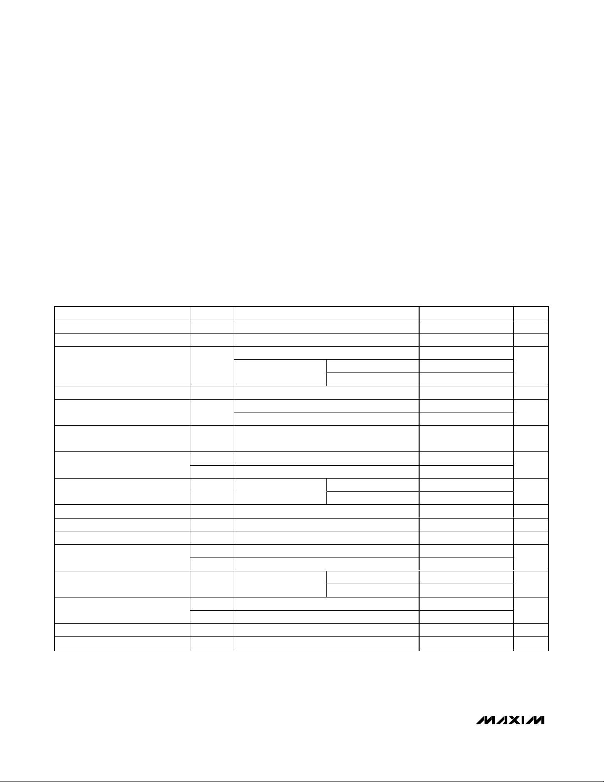
ELECTRICAL CHARACTERISTICS
(VIN= 3.6V, SHDN = IN, TA= -40°C to +85°C, typical values are at TA= +25°C, unless otherwise noted.) (Note 2)
)
)
Note 1: LX has internal clamp diodes to IN and GND. Applications that forward bias these diodes should not exceed the IC’s package
power-dissipation limit.
Note 2: All devices are 100% production tested at T
A
= +25°C. Limits over the operating temperature range are guaranteed by design.
Supply Range V
UVLO Threshold UVLO VIN rising, 100mV hysteresis 2.44 2.6 2.70 V
Supply Current I
Output Voltage Range V
Output Voltage Accuracy
(Falling Edge)
Output Load Regulation
(Voltage Positioning)
SHDN Logic Input Level
SHDN Logic Input Bias Current I
Peak Current Limit I
Valley Current Limit I
Rectifier Off-Current Threshold I
On-Resistance
LX Leakage Current I
Minimum On and Off Times
Thermal Shutdown +160 °C
Thermal-Shutdown Hysteresis 20 °C
PARAMETER
SYMBOL CONDITIONS MIN TYP MAX UNITS
IN
No load, no switching 24 48
CC
SHDN = GND
OUT
V
V
IH,IL
LIMP
LIMN
LXOFF
R
ONP
R
ONN
LXLKG
t
ON(MIN
t
OFF(MIN
Factory preset 0.8 2.5 V
I
= 0mA, TA = +25°C -1 0 +1
LOAD
I
= 0mA, TA = -40°C to +85°C -2 +2
LOAD
Equal to inductor DC resistance R
VIN = 2.7V to 4.9V 1.4
IH
VIN = 2.7V to 4.9V 0.4
IL
VIN = 4.9V,
SHDN = GND or IN
pFET switch 590 770 1400 mA
nFET rectifier 450 650 1300 mA
nFET rectifier 10 40 70 mA
pFET switch, ILX = -40mA 0.6 1.2
nFET rectifier, ILX = 40mA 0.35 0.7
V
= 4.9V, LX = GND
IN
to IN, SHDN = GND
2.7 4.9 V
TA = +25°C 0.01 0.1
T
= +85°C 0.1
A
L
TA = +25°C 0.001 1
= +85°C 0.01
T
A
TA = +25°C 0.1 1
T
= +85°C 1
A
95
95
µA
%
V/A
V
µA
Ω
µA
ns
Page 3
MAX8640Y/MAX8640Z
500mA, 4MHz/2MHz Synchronous
Step-Down DC-DC Converters in SC70
_______________________________________________________________________________________ 3
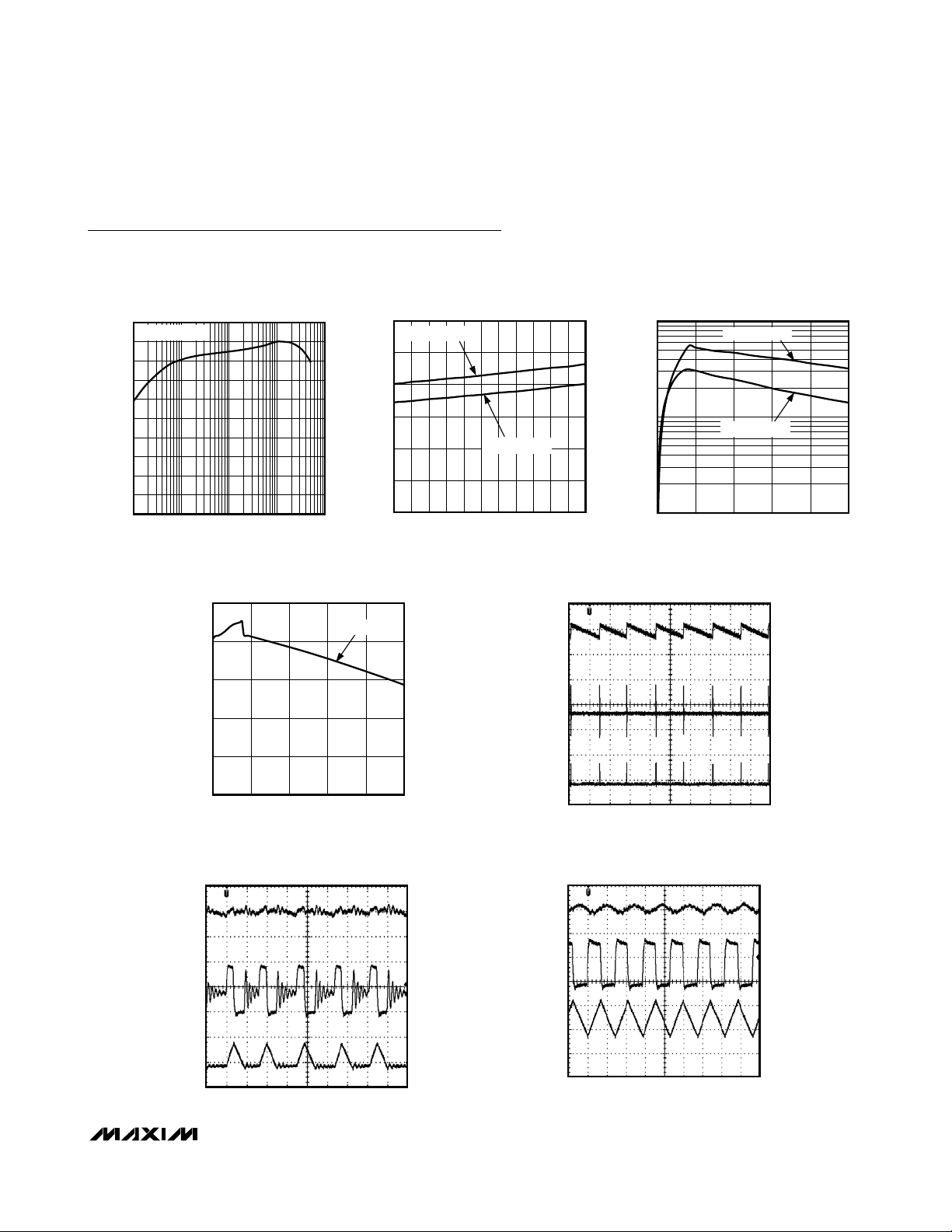
Typical Operating Characteristics
(VIN= 3.6V, V
OUT
= 1.5V, MAX8640Z, L = Murata LQH32CN series, TA= +25°C, unless otherwise noted.)
EFFICIENCY vs. LOAD CURRENT
1.8V OUTPUT
LOAD CURRENT (mA)
EFFICIENCY (%)
MAX8640Y/Z toc01
0
10
20
30
40
50
60
70
80
90
100
0.1 1 10 100 1000
MAX8640YEXT18
NO-LOAD SUPPLY CURRENT
vs. SUPPLY VOLTAGE
SUPPLY VOLTAGE (V)
SUPPLY CURRENT (μA)
MAX8640Y/Z toc02
2.9 3.3 3.7 4.1 4.5 4.9
5
10
15
20
25
30
35
MAX8640ZEXT15
MAX8640YEXT18
SWITCHING FREQUENCY
vs. LOAD CURRENT
LOAD CURRENT (mA)
SWITCHING FREQUENCY (MHz)
MAX8640Y/Z toc03
0 100 200 300 400 500
0.1
1
10
MAX8640ZEXT15
MAX8640YEXT18
OUTPUT VOLTAGE vs. LOAD CURRENT
(VOLTAGE POSITIONING)
LOAD CURRENT (mA)
OUTPUT VOLTAGE (V)
MAX8640Y/Z toc04
0 100 200 300 400 500
1.30
1.35
1.40
1.45
1.50
1.55
MAX8640ZEXT15
I
LX
V
LX
V
OUT
200mA/div
2V/div
20mV/div
(AC-COUPLED)
10μs/div
LIGHT-LOAD SWITCHING WAVEFORMS
(I
OUT
= 1mA)
MAX8640Y/Z toc05
I
LX
V
LX
V
OUT
200mA/div
2V/div
0V
0mA
20mV/div
(AC-COUPLED)
200ns/div
MEDIUM-LOAD SWITCHING WAVEFORMS
(I
OUT
= 40mA)
MAX8640Y/Z toc06
I
LX
V
LX
V
OUT
200mA/div
2V/div
0V
0mA
20mV/div
(AC-COUPLED)
200ns/div
HEAVY-LOAD SWITCHING WAVEFORMS
(I
OUT
= 300mA)
MAX8640Y/Z toc07
Page 4

MAX8640Y/MAX8640Z
500mA, 4MHz/2MHz Synchronous
Step-Down DC-DC Converters in SC70
4 _______________________________________________________________________________________
Typical Operating Characteristics (continued)
(VIN= 3.6V, V
OUT
= 1.5V, MAX8640Z, L = Murata LQH32CN series, TA= +25°C, unless otherwise noted.)
I
LX
I
IN
V
SHDN
V
OUT
100mA/div
500mA/div
1V/div
0V
0mA
0mA
5V/div
20μs/div
LIGHT-LOAD STARTUP WAVEFORM
(100Ω LOAD)
MAX8640Y/Z toc08
I
LX
I
IN
V
SHDN
V
OUT
100mA/div
500mA/div
1V/div
0V
0mA
0mA
5V/div
20μs/div
HEAVY-LOAD STARTUP WAVEFORM
(5Ω LOAD)
MAX8640Y/Z toc09
I
LX
V
OUT
V
IN
20mV/div
AC-COUPLED
200mA/div
0mA
1V/div
4V
20μs/div
LINE-TRANSIENT RESPONSE
(4V TO 3.5V TO 4V)
MAX8640Y/Z toc10
I
OUT
V
OUT
I
LX
500mA/div
50m/div
AC-COUPLED
200mA/div
0mA
40μs/div
LOAD-TRANSIENT RESPONSE
(5mA TO 250mA TO 5mA)
MAX8640Y/Z toc11
I
OUT
V
OUT
I
LX
500mA/div
100mV/div
AC-COUPLED
200mA/div
0V
40μs/div
LOAD-TRANSIENT RESPONSE
(10mA TO 500mA TO 10mA)
MAX8640Y/Z toc12
Page 5

MAX8640Y/MAX8640Z
500mA, 4MHz/2MHz Synchronous
Step-Down DC-DC Converters in SC70
_______________________________________________________________________________________ 5
Pin Description
Detailed Description
The MAX8640Y/MAX8640Z step-down converters deliver over 500mA to outputs from 0.8V to 2.5V. They utilize
a proprietary hysteretic PWM control scheme that
switches at up to 4MHz (MAX8640Z) or 2MHz
(MAX8640Y), allowing some trade-off between efficiency and size of external components. At loads below
100mA, the MAX8640Y/MAX8640Z automatically switch
to pulse-skipping mode to minimize the typical quiescent current (24µA). Output ripple remains low at all
loads, while the skip-mode switching frequency
remains ultrasonic down to 1mA (typ) loads. Figure 1 is
the simplified functional diagram.
Control Scheme
A proprietary hysteretic PWM control scheme ensures
high efficiency, fast switching, fast transient response,
low output ripple, and physically tiny external components. This control scheme is simple: when the output
voltage is below the regulation threshold, the error
comparator begins a switching cycle by turning on the
high-side switch. This switch remains on until the minimum on-time expires and the output voltage is above
the regulation threshold or the inductor current is above
the current-limit threshold. Once off, the high-side
switch remains off until the minimum off-time expires
and the output voltage falls again below the regulation
threshold. During the off period, the low-side synchronous rectifier turns on and remains on until either the
high-side switch turns on again or the inductor current
approaches zero. The internal synchronous rectifier
eliminates the need for an external Schottky diode.
Voltage-Positioning Load Regulation
The MAX8640Y/MAX8640Z utilize a unique feedback
network. By taking DC feedback from the LX node, the
usual phase lag due to the output capacitor is
removed, making the loop exceedingly stable and
allowing the use of very small ceramic output capacitors.
This configuration yields load regulation equal to the
inductor’s series resistance multiplied by the load current.
This voltage-positioning load regulation greatly reduces
overshoot during load transients, effectively halving the
peak-to-peak output-voltage excursions compared to traditional step-down converters. See the Load-Transient
Response in the Typical Operating Characteristics.
Shutdown Mode
Connecting SHDN to GND or logic low places the
MAX8640Y/MAX8640Z in shutdown mode and reduces
supply current to 0.1µA (typ). In shutdown, the control
circuitry and internal MOSFET switches turn off and LX
becomes high impedance. Connect SHDN to IN or
logic high for normal operation.
Figure 1. Simplified Functional Diagram
PIN NAME FUNCTION
1LX
2, 5 GND Ground. Connect these pins together directly under the IC.
3 OUT
4 SHDN
6IN
Inductor Connection to the Internal Drains of the p-channel and n-channel MOSFETs. High impedance
during shutdown.
Output Sense Input. Bypass with a ceramic capacitor as close as possible to pin 3 (OUT) and pin 2 (GND).
OUT is internally connected to the internal feedback network.
Active-Low Shutdown Input. Connect to IN or logic-high for normal operation. Connect to GND or logic-low for
shutdown mode.
Supply Voltage Input. Input voltage range is 2.7V to 4.9V. Bypass with a ceramic capacitor as close as
possible to pin 6 (IN) and pin 5 (GND).
SHDN
PWM
LOGIC
MAX8640Y
MAX8640Z
IN
LX
GND
OUT
0.6V
Page 6

Soft-Start
The MAX8640Y/MAX8640Z include internal soft-start
circuitry that eliminates inrush current at startup, reducing transients on the input source. Soft-start is particularly useful for higher impedance input sources, such
as Li+ and alkaline cells. See the Soft-Start Response
in the Typical Operating Characteristics.
Applications Information
The MAX8640Y/MAX8640Z are optimized for use with a
tiny inductor and small ceramic capacitors. The correct
selection of external components ensures high efficiency, low output ripple, and fast transient response.
Inductor Selection
A 1µH inductor is recommended for use with the
MAX8640Z, and 2.2µH is recommended for the
MAX8640Y. A 1µH inductor is physically smaller but
requires faster switching, resulting in some efficiency
loss. Table 1 lists several recommended inductors.
It is acceptable to use a 1.5µH inductor with either the
MAX8640Y or MAX8640Z, but efficiency and ripple
should be verified. Similarly, it is acceptable to use a
3.3µH inductor with the MAX8640Y, but performance
should be verified.
For optimum voltage positioning of load transients,
choose an inductor with DC series resistance in the
75mΩ to 150mΩ range. For higher efficiency at heavy
loads (above 200mA) or minimal load regulation (but
some transient overshoot), the resistance should be
kept as low as possible. For light-load applications up
to 200mA, higher resistance is acceptable with very little impact on performance.
MAX8640Y/MAX8640Z
500mA, 4MHz/2MHz Synchronous
Step-Down DC-DC Converters in SC70
6 _______________________________________________________________________________________
Table 1. Suggested Inductors
MANUFACTURER SERIES
MIPFT2520D 2.0 0.16 900 2.5 x 2.0 x 0.5
FDK
Sumida CDRH2D09
Taiyo Yuden CKP3216T
TDK
TOKO
MIPF2520D
GLF201208T
GLF2012T
GLF251812T
MDT2520-CR
D2812C
INDUCTANCE
(µH)
1.5 0.07 1500
2.2 0.08 1300
3.3 0.10 1200
1.0 0.12 1200
1.5 0.16 1000Murata LQM31P
2.2 0.22 900
1.2 0.08 590
1.5 0.09 520
2.2 0.12 440
1.0 0.11 1100
1.5 0.13 1000
2.2 0.14 900
1.0 0.15 460
2.2 0.36 300
1.0 0.07 400
2.2 0.10 300
1.0 0.10 800
2.2 0.20 600
1.0 0.05 1000
2.2 0.08 700
1.0 0.07 1100
2.2 0.14 770
DC RESISTANCE
(Ω typ)
CURRENT RATING
(mA)
DIMENSIONS
L x W x H (mm)
2.5 x 2.0 x 1.0
3.2 x 1.6 x 0.95
3.0 x 3.0 x 1.0
3.2 x 1.6 x 0.9
2.0 x 1.25 x 0.9
2.0 x 1.25 x 1.35
2.5 x 1.8 x 1.35
2.5 x 2.0 x 1.0
2.8 x 2.8 x 1.2
Page 7

MAX8640Y/MAX8640Z
500mA, 4MHz/2MHz Synchronous
Step-Down DC-DC Converters in SC70
_______________________________________________________________________________________ 7
Capacitor Selection
Output Capacitor
The output capacitor, C2, is required to keep the output
voltage ripple small and to ensure regulation loop stability. C2 must have low impedance at the switching
frequency. Ceramic capacitors are recommended due
to their small size and low ESR. Make sure the capacitor maintains its capacitance over temperature and DC
bias. Capacitors with X5R or X7R temperature characteristics typically perform well. The output capacitance
can be very low; see the Selector Guide for recommended capacitance values. For optimum load-transient performance and very low output ripple, the
output capacitor value in µF should be equal to or larger than the inductor value in µH.
Input Capacitor
The input capacitor, C1, reduces the current peaks
drawn from the battery or input power source and
reduces switching noise in the IC. The impedance of
C1 at the switching frequency should be kept very low.
Ceramic capacitors are recommended due to their
small size and low ESR. Make sure the capacitor main-
tains its capacitance over temperature and DC bias.
Capacitors with X5R or X7R temperature characteristics typically perform well. Due to the MAX8640Y/
MAX8640Z soft-start, the input capacitance can be
very low. For optimum noise immunity and low input ripple, choose a capacitor value in µF that is equal to or
larger than the inductor’s value in µH.
PC Board Layout and Routing
High switching frequencies and large peak currents
make PC board layout a very important part of design.
Good design minimizes excessive EMI on the feedback
paths and voltage gradients in the ground plane, both
of which can result in instability or regulation errors.
Connect the inductor, input capacitor, and output
capacitor as close together as possible, and keep their
traces short, direct, and wide. Connect the two GND
pins under the IC and directly to the grounds of the
input and output capacitors. Keep noisy traces, such
as the LX node, as short as possible. Refer to the
MAX8640Z evaluation kit for an example PC board layout and routing scheme.
Selector Guide
PART
MAX8640YEXT08 0.8 1.2 2.2
MAX8640YEXT11 1.1 1.7 2.2
MAX8640YEXT12 1.2 1.8 2.2
MAX8640YEXT13 1.3 1.9 2.2
MAX8640YEXT15 1.5 2.0 2.2
MAX8640YEXT16 1.6 2.0 2.2
MAX8640YEXT18 1.8 2.0 2.2
MAX8640YEXT19 1.9 2.0 2.2
MAX8640YEXT25 2.5 1.7 2.2
MAX8640ZEXT08 0.8 2.4 1
MAX8640ZEXT11 1.1 3.4 1
MAX8640ZEXT12 1.2 3.6 1
MAX8640ZEXT13 1.3 3.7 1
MAX8640ZEXT15 1.5 3.9 1
MAX8640ZEXT18 1.8 4.0 1
OUTPUT
VOLTAGE (V)
FREQUENCY
(MHz)
RECOMMENDED COMPONENTS
L1 (µH)
C2 (µF)
10
4.7
4.7
4.7
4.7
4.7
4.7
4.7
4.7
4.7
2.2
2.2
2.2
2.2
2.2
TOP MARK
ACQ
ACR
ACS
ACG
ADD
ADB
ACI
ACH
ACJ
ACL
ACM
ACN
ACO
ACP
ACU
Page 8

MAX8640Y/MAX8640Z
500mA, 4MHz/2MHz Synchronous
Step-Down DC-DC Converters in SC70
8 _______________________________________________________________________________________
Chip Information
PROCESS: BiCMOS
Ordering Information (continued)
*Contact factory for availability of each version.
Note: All devices are specified over the -40°C to +85°C
operating temperature range.
PART*
MAX8640ZEXT08+T 6 SC70-6 X6S-1
MAX8640ZEXT11+T 6 SC70-6 X6S-1
MAX8640ZEXT12+T 6 SC70-6 X6S-1
MAX8640ZEXT13+T 6 SC70-6 X6S-1
MAX8640ZEXT15+T 6 SC70-6 X6S-1
MAX8640ZEXT18+T 6 SC70-6 X6S-1
PINPACKAGE
PKG
CODE
TOP
MARK
ACL
ACM
ACN
ACO
ACP
ACU
Page 9

MAX8640Y/MAX8640Z
500mA, 4MHz/2MHz Synchronous
Step-Down DC-DC Converters in SC70
Maxim cannot assume responsibility for use of any circuitry other than circuitry entirely embodied in a Maxim product. No circuit patent licenses are
implied. Maxim reserves the right to change the circuitry and specifications without notice at any time.
Maxim Integrated Products, 120 San Gabriel Drive, Sunnyvale, CA 94086 408-737-7600 _____________________ 9
© 2006 Maxim Integrated Products Printed USA is a registered trademark of Maxim Integrated Products, Inc.
Package Information (continued)
(The package drawing(s) in this data sheet may not reflect the most current specifications. For the latest package outline information,
go to www.maxim-ic.com/packages
.)
SC70, 6L.EPS
PACKAGE OUTLINE, 6L SC70
1
21-0077
D
1
 Loading...