

Page 1
_______________General Description
The MAX863 dual-output DC-DC converter contains
two independent step-up controllers in a single compact package. This monolithic Bi-CMOS design draws
only 85µA when both controllers are on. The input
range extends down to 1.5V, permitting use in organizers, translators, and other low-power hand-held products. The MAX863 provides 90% efficiency at output
loads from 20mA to over 1A. This space-saving device
is supplied in a 16-pin QSOP package that fits in the
same area as an 8-pin SOIC.
The device uses a current-limited, pulse-frequencymodulated (PFM) control architecture that reduces startup surge currents and maintains low quiescent currents
for excellent low-current efficiency. Each controller
drives a low-cost, external, N-channel MOSFET switch,
whose size can be optimized for any output current or
voltage.
In larger systems, two MAX863s can be used to generate 5V, 3.3V, 12V, and 28V from just two or three battery cells. An evaluation kit (MAX863EVKIT) is available
to speed designs. For a single-output controller, refer to
the MAX608 and MAX1771 data sheets.
________________________Applications
2- and 3-Cell Portable Equipment
Organizers
Translators
Hand-Held Instruments
Palmtop Computers
Personal Digital Assistants (PDAs)
Dual Supply (Logic and LCD)
____________________________Features
♦ Smallest Dual Step-Up Converter: 16-Pin QSOP
♦ 90% Efficiency
♦ 1.5V Start-Up Voltage
♦ 85µA Max Total Quiescent Supply Current
♦ 1µA Shutdown Mode
♦ Independent Shutdown Inputs
♦ Drives Surface-Mount, Dual N-Channel MOSFETs
♦ Low-Battery Input/Output Comparator
♦ Step-Up/Down Configurable
MAX863
Dual, High-Efficiency, PFM, Step-Up
DC-DC Controller
________________________________________________________________ Maxim Integrated Products 1
__________________Pin Configuration
16
15
14
13
12
11
10
9
1
2
3
4
5
6
7
8
SENSE1 REF
SHDN2
LBI
LBO
FB2
SHDN1
CS2
EXT2
TOP VIEW
MAX863
QSOP
V
DD
FB1
EXT1
BOOT
CS1
GND
PGND
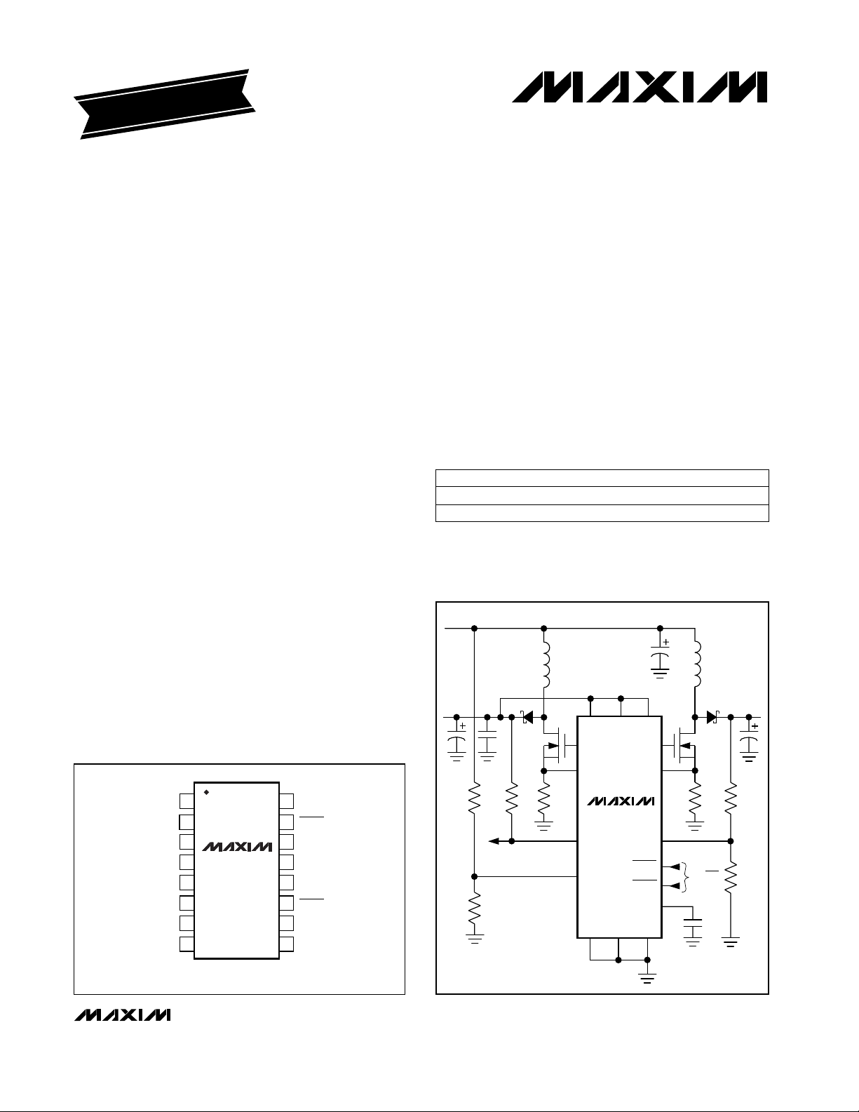
__________Typical Operating Circuit
19-1218; Rev 2; 2/98
PART
MAX863C/D
MAX863EEE -40°C to +85°C
0°C to +70°C
TEMP. RANGE PIN-PACKAGE
Dice*
16 QSOP
EVALUATION KIT MANUAL
AVAILABLE
______________Ordering Information
*Dice are tested at TA= +25°C.
For pricing, delivery, and ordering information, please contact Maxim/Dallas Direct! at
1-888-629-4642, or visit Maxim’s website at www.maxim-ic.com.
V
IN
OUT1
SENSE1 V
N
EXT1
CS1
BOOT
DD
EXT2
CS2
OUT2
N
MAX863
PGND
FB2
SHDN1
SHDN2
REF
GND
ON/OFF
LOW-BATTERY
DETECTOR OUTPUT
LBO
LBI
FB1
Page 2
MAX863
Dual, High-Efficiency, PFM, Step-Up
DC-DC Controller
2 _______________________________________________________________________________________
ABSOLUTE MAXIMUM RATINGS
ELECTRICAL CHARACTERISTICS
(VDD= +5V, I
LOAD
= 0mA, TA= 0°C to +85°C, unless otherwise noted. Typical values are at TA= +25°C.)
Stresses beyond those listed under “Absolute Maximum Ratings” may cause permanent damage to the device. These are stress ratings only, and functional
operation of the device at these or any other conditions beyond those indicated in the operational sections of the specifications is not implied. Exposure to
absolute maximum rating conditions for extended periods may affect device reliability.
VDDto GND............................................................-0.3V to +12V
PGND to GND .......................................................-0.3V to +0.3V
SHDN1, SHDN2, SENSE1, LBO to GND ................-0.3V to +12V
EXT1, EXT2 to PGND..................................-0.3V to (V
DD
+ 0.3V)
FB1, FB2, CS1, CS2, SEL,
LBI, BOOT to GND.................................-0.3V to (V
DD
+ 0.3V)
LBO Continuous Output Current.........................................15mA
EXT1, EXT2 Continuous Output Current .............................50mA
Continuous Power Dissipation (T
A
= +70°C)
QSOP (derate 8.30mW/°C above +70°C) ...................667mW
Operating Temperature Range
MAX863EEE ....................................................-40°C to +85°C
Junction Temperature......................................................+150°C
Storage Temperature Range .............................-65°C to +160°C
Lead Temperature (soldering, 10sec) .............................+300°C
V
DD
= OUT1 = BOOT (Note 1)
CONDITIONS
1.5 11
UNITSMIN TYP MAXSYMBOLPARAMETER
(Note 2)
V
2.7 11
V
DD
VDDInput Voltage
SHDN1 = VDD, SHDN2 = GND,
measured from V
DD
µA
35 60
I
DD
Quiescent Current
SHDN1 = SHDN2 = VDD, measured from V
DD
50 85
VIN= 2.7V to 5V, V
OUT1
= 5V,
I
LOAD
= 300mA, Figure 2
mV/V8Line Regulation
VIN= 3.3V, V
OUT1
= 5V,
I
LOAD
= 0mA to 500mA, Figure 2
mV/A40Load Regulation
nA210IFB, I
LBI
FB1, FB2, LBI Input Current
VDD= 1.5V
V
0.7 x V
DD
V
IH
2.7V < VDD< 11V 1.6
SHDN1, SHDN2, SEL, BOOT
Input High Voltage
mV85 100 115V
CS
CS1, CS2 Threshold Voltage
µs14 17.5 22
Logic input = VDDor GND
t
ON
Maximum Switch On-Time
µA125CS1, CS2 Input Current
µA1I
I
SHDN1, SHDN2, SEL, BOOT
Input Current
V1.225 1.25 1.275VFB, V
LBI
FB1, FB2, LBI
Threshold Voltage (Note 4)
C
LOAD
= 1nF, 10% to 90% ns50EXT Rise/Fall Time (Note 5)
µs1.6 2 2.4t
OFF
Minimum Switch Off-Time
FB1 = GND
V
4.85 5 5.15
V
OUT1
OUT1 Output Voltage
(Note 3)
FB1 = V
DD
3.2 3.3 3.4
VDD= 1.5V
V
0.2 x V
DD
V
IL
2.7V < VDD< 11V 0.4
SHDN1, SHDN2, SEL, BOOT
Input Low Voltage
SHDN1 = SHDN2 = GND
µA1I
DD, SHDN
Shutdown Current
Ω
5EXT On-Resistance
V
LBO
= 11V, V
LBI
> 1.275V µA1I
LBO
LBO Leakage Current
I
LBO,SINK
= 1mA, V
LBI
< 1.225V V0.1 0.4V
LBO,L
LBO Low Level
Page 3
MAX863
Dual, High-Efficiency, PFM, Step-Up
DC-DC Controller
_______________________________________________________________________________________ 3
ELECTRICAL CHARACTERISTICS
(VDD= +5V, I
LOAD
= 0mA, TA= -40°C to +85°C, unless otherwise noted.) (Note 6)
Note 1: When bootstrapped, an internal low-voltage oscillator drives the EXT1 pin rail-to-rail for low supply voltages.
Note 2: For non-bootstrapped operation, V
DD
> 2.7V is required to allow valid operation of all internal circuitry.
Note 3: For adjustable output voltages, see the Set the Output Voltage section.
Note 4: Measured with LBI falling. Typical hysteresis is 15mV.
Note 5: EXT1 and EXT2 swing from V
DD
to GND.
Note 6: Specifications to -40°C are guaranteed by design and not production tested.
VDD= OUT1 (Note 1) 1.6 11
CONDITIONS
VDDInput Voltage
(Note 2)
V
2.8 11
V
DD
V1.21 1.285V
FB
FB1, FB2 Threshold Voltage
60
mV85 115V
CS
CS1, CS2 Threshold Voltage
UNITSMIN TYP MAXSYMBOLPARAMETER
FB1 = V
DD
3.15 3.45
OUT1 Output Voltage
(Note 3)
FB1 = GND
V
4.8 5.2
V
OUT1
SHDN1 = SHDN2 = VDD, measured from V
DD
85
Quiescent Current
SHDN1 = VDD, SHDN2 = GND,
measured from V
DD
µAI
DD
SHDN1 = SHDN2 = GND
µA1I
DD, SHDN
Shutdown Current
__________________________________________Typical Operating Characteristics
(TA = +25°C, unless otherwise noted.)
0.01 0.1 1 10 100 1000
EFFICIENCY vs. OUTPUT CURRENT
(V
OUT1
= 3.3V, BOOTSTRAPPED)
MAX863 toc01
OUTPUT CURRENT (mA)
EFFICIENCY (%)
B
C
A
10
0
30
20
50
40
70
60
90
80
100
V
OUT1
= 3.3V
A: V
IN
= 1.5V
B: V
IN
= 2.4V
C: V
IN
= 2.7V
0.01 0.1
10
0
30
20
50
40
70
60
90
80
100
1 10 100 1000
EFFICIENCY vs. OUTPUT CURRENT
(V
OUT1
= 5.0V, BOOTSTRAPPED)
MAX863 toc02
OUTPUT CURRENT (mA)
EFFICIENCY (%)
V
OUT1
= 5.0V
A: V
IN
= 1.5V
B: V
IN
= 2.4V
C: V
IN
= 2.7V
D: V
IN
= 3.3V
E: V
IN
= 3.6V
F: V
IN
= 4.0V
B
C
A
D
E
F
0.01 0.1
0
10
20
30
40
50
60
70
80
90
100
1 10 100 1000
EFFICIENCY vs. OUTPUT CURRENT
(V
OUT1
= 5.0V, NON-BOOTSTRAPPED)
MAX863 toc03
OUTPUT CURRENT (mA)
EFFICIENCY (%)
V
OUT1
= 5.0V
A: V
IN
= 2.7V
B: V
IN
= 3.3V
C: V
IN
= 3.6V
D: V
IN
= 4.0V
A
B
C
D
Page 4
MAX863
Dual, High-Efficiency, PFM, Step-Up
DC-DC Controller
4 _______________________________________________________________________________________
____________________________Typical Operating Characteristics (continued)
(TA = +25°C, unless otherwise noted.)
0.01 0.1
10
20
30
40
50
60
70
80
90
100
0
1 10 100 1000
EFFICIENCY vs. OUTPUT CURRENT
(V
OUT1
= 12V, NON-BOOTSTRAPPED)
MAX863 toc04
OUTPUT CURRENT (mA)
EFFICIENCY (%)
V
OUT1
= 5.0V
A: V
IN
= 2.7V
B: V
IN
= 3.3V
C: V
IN
= 3.6V
D: V
IN
= 4.0V
E: V
IN
= 6.0V
A
B
C
D
E
3.5
1
1 10 1000
BOOTSTRAPPED-MODE MINIMUM
START-UP INPUT VOLTAGE
vs. OUTPUT CURRENT
0.5
1.0
1.5
2.0
2.5
3.0
MAX863toc05
OUTPUT CURRENT (mA)
START-UP INPUT VOLTAGE (V)
100
V
OUT1
= 3.3V
V
OUT1
= 5V
0
012
VDD CURRENT
vs. V
DD
VOLTAGE
10
20
60
MAX863 toc15
VDD VOLTAGE (V)
V
DD
CURRENT (µA)
40
30
8
50
10
24 6
Cond: Single +5V
BOTH ON
CONVERTER 1 ON
CONVERTER 2 ON
LOAD-TRANSIENT RESPONSE
A
MAX863 toc08
B
100µs/div
V
OUT1
= 3.3V, I
OUT1
= 100mA TO 600mA
A: V
OUT1
, 100mV/div, 3.3V DC OFFSET
B: I
OUT1
, 200mA/div
RESPONSE ENTERING/
EXITING SHUTDOWN (BOOTSTRAPPED)
B
A
MAX863 toc09
C 3.3V
200µs/div
V
OUT1
= 3.3V, I
OUT1
= 100mA, VIN = 2.4V
A: SHDN1, 5V/div
B: INDUCTOR CURRENT, 2A/div
C: V
OUT1
, 3.3V OFFSET, 500mV/div
LINE-TRANSIENT RESPONSE
B
A
MAX863 toc10
C0A
500µs/div
V
OUT1
= 5V, I
OUT1
= 800mA
A: V
IN
= 2.7V TO 3.7V, 500mV/div
B: V
OUT1
, AC COUPLED, 50mV/div
C: INDUCTOR CURRENT, 2A/div
0
012
EXT RISE AND FALL TIMES vs.
SUPPLY VOLTAGE AND MOSFET CAPACITANCE
20
140
MAX863 toc07
SUPPLY VOLTAGE (V)
RISE/FALL TIME (ns)
6
60
80
40
24 8
120
100
C,1
C,2
B,1
B,2
A,1
A,2
10
A: 470pF
B: 1.0nF
C: 2.2nF
1: RISE
2: FALL
Page 5
MAX863
Dual, High-Efficiency, PFM, Step-Up
DC-DC Controller
_______________________________________________________________________________________ 5
_______________Detailed Description
The MAX863 dual, bi-CMOS, step-up, switch-mode
power-supply controller provides preset 3.3V, 5V, or
adjustable outputs. Its pulse-frequency-modulated
(PFM) control scheme combines the advantages of low
supply current at light loads and high efficiency with
heavy loads. These attributes make the MAX863 ideal
for use in portable battery-powered systems where
small size and low cost are extremely important, and
where low quiescent current and high efficiency are
needed to maximize operational battery life. Use of
external current-sense resistors and MOSFETs allows
the designer to tailor the output current and voltage
capability for a diverse range of applications.
PFM Control Scheme
Each DC-DC controller in the MAX863 uses a one-shotsequenced, current-limited PFM design, as shown in
Figure 1. Referring to the Typical Operating Circuit
(Figure 2) and the switching waveforms (Figures 3a–3f),
the circuit works as follows. Output voltage is sensed
by the error comparator using either an internal voltage
divider connected to SENSE1 or an external voltage
divider connected to FB1. When the output voltage
drops, the error comparator sets an internal flip-flop.
The flip-flop turns on an external MOSFET, which allows
inductor current to ramp-up, storing energy in a magnetic field.
______________________________________________________________Pin Description
PIN
Feedback Input for DC-DC Controller 1 in Fixed-Output ModeSENSE11
FUNCTIONNAME
IC Power-Supply InputV
DD
2
Bootstrap Low-Voltage-Oscillator Enable Input. BOOT is an active-high, logic-level input. It enables the
low-voltage oscillator to allow start-up from input voltages down to 1.5V while in a bootstrapped circuit
configuration. Connect BOOT to GND when in a non-bootstrapped configuration. If BOOT is high, V
DD
must be connected to OUT1.
BOOT4
Adjustable Feedback and Preset Output Voltage Selection Input for DC-DC Controller 1. Connect to V
DD
for 3.3V preset output or to GND for 5V output. Connect a resistor voltage divider to adjust the output voltage. See the section Set the Output Voltage.
FB13
Gate-Drive Output of DC-DC Controller 1. Drives an external N-channel power MOSFET.EXT16
High-Current Ground Return for Internal MOSFET DriversPGND8
Analog Ground for Internal Reference, Feedback, and Control CircuitsGND7
Input to the Current-Sense Comparator of DC-DC Controller 1CS15
Input to the Current-Sense Amplifier of DC-DC Controller 2CS210
Adjustable Feedback Input for DC-DC Controller 2. Connect a resistor voltage divider to adjust the output
voltage. See the section Set the Output Voltage.
FB212
Active-Low Shutdown Input for DC-DC Controller 1. Connect to VDDfor normal operation.
SHDN1
11
Low-Battery Comparator Input. When the voltage on LBI drops below 1.25V, LBO sinks current. If unused,
connect to GND.
LBI14
Reference Bypass Input. Connect a 0.1µF ceramic capacitor from REF to GND.REF16
Active-Low Shutdown Input for DC-DC Controller 2. Connect to VDDfor normal operation.
SHDN2
15
Low-Battery Output. An open-drain N-channel MOSFET output. Sinks current when the voltage on LBI
drops below 1.25V. If unused, connect to GND.
LBO13
Gate-Drive Output of DC-DC Controller 2. Drives an external N-channel power MOSFET.EXT29
Page 6

MAX863
Dual, High-Efficiency, PFM, Step-Up
DC-DC Controller
6 _______________________________________________________________________________________
The flip-flop resets and turns off the MOSFET when
either a) the voltage across the current-sense resistor
exceeds 100mV, or b) the 17.5µs maximum on-time
one-shot trips. When the MOSFET turns off, the magnetic field begins to collapse, and forces current into
the output capacitor and load. As the stored energy is
transferred to the output, the inductor current ramps
down. The output capacitor smoothes out the energy
transfer by storing charge when the diode current is
high, then supplying current to the load during the first
half of each cycle, maintaining a steady output voltage.
Resetting the flip-flop sets the off-time one-shot, disabling the error-comparator output and forcing the
MOSFET off for at least 2µs to enforce a minimum time
for energy transfer to the output. The MAX863 waits
until the output voltage drops again before beginning
another cycle. The MAX863’s switching frequency
depends on the load current and input voltage.
Figure 1. Functional Diagram
FB2
CS2
CS1
SENSE1
FB1
V
DD
100mV
- 100mV
REF
100mV
ERROR
COMPARATOR
CURRENT-SENSE
COMPARATOR
TRIG
MIN ON-TIME
ONE-SHOT
100mV
REF
Q
Q
MAX ON-TIME
ONE-SHOT
CURRENT-
SENSE
COMPARATOR
ERROR
COMPARATOR
TRIG
S
Q
R
OSCILLATOR
TIMING
BLOCK
LOW-
VOLTAGE
TIMING
BLOCK
MAX863
UVLO
EXT2
PGND
BOOT
EXT1
V
DD
LBO
LBI
REF
N
N
V
DD
REF
1.25V
GND SHDN2 SHDN1REF
BIAS
Page 7

MAX863
Dual, High-Efficiency, PFM, Step-Up
DC-DC Controller
_______________________________________________________________________________________ 7
Continuous/Discontinuous-Conduction
Modes
Each converter in the MAX863 determines from moment
to moment whether to switch or not, waiting until the output voltage drops before initiating another cycle. Under
light loads, the inductor current ramps to zero before the
next cycle; this is discontinuous-conduction mode.
Continuous-conduction mode occurs when the next
switching cycle begins while current is still flowing
through the inductor. The transition point between discontinuous- and continuous-conduction mode is determined by input and output voltages, and by the size of
the inductor relative to the peak switching current. In
general, reducing inductance toward the minimum recommended value pushes the transition point closer to
the maximum load current. If the inductor value is low
enough or the output/input voltage ratio high enough,
the DC-DC converter may remain in discontinuous-conduction mode throughout its entire load range.
The MAX863 transitions into continuous-conduction
mode in two ways, depending on whether preset or
adjustable mode is used and how the external feedback network is compensated. Under light loads, the IC
switches in single pulses (Figure 3a). The threshold of
transition into continuous-conduction mode is reached
when the inductor current waveforms are adjacent to
one another, as shown in Figure 3b. As the load
increases, the transition into continuous-conduction
mode progresses by raising the minimum inductor current (Figures 3c, 3d). Depending on feedback compensation, transition into continuous-conduction mode may
also progress with grouped pulses (Figures 3e, 3f).
Pulse groups should be separated by less than two or
three switching cycles. Output ripple should not be
significantly more than the single-cycle no-load case.
V
Figure 2. Bootstrapped Typical Operating Circuit
= 1.5V TO THE LOWER OF V
IN
V
= 5V
OUT1
C1
220µF
10V
≤0.1Ω
R5
OR V
OUT1
OUT2
C4
100µF
10V
≤0.1Ω
BOOT
DD
EXT2
CS2
50mΩ
R2
L2
10µH
2A
MBRS340T3
N1B
IRF7301
D2
V
= 3.3V
OUT2
C5
330µF
10V
≤0.1Ω
R3
165k
1%
C6
10pF
C2
0.1µF
100k
R7
D1
MBRS340T3
L1
10µH
2A
R1
50mΩ
N1A
C3
100µF
10V
≤0.1Ω
SENSE1 V
EXT1
CS1
MAX863
LOW-BATTERY
DETECTOR OUTPUT
R6
LBO
LBI
FB1
PGND
FB2
SHDN1
SHDN2
REF
GND
ON/OFF
C7
0.1µF
R4
100k
1%
Page 8

MAX863
Dual, High-Efficiency, PFM, Step-Up
DC-DC Controller
8 _______________________________________________________________________________________
Figure 4a. Non-Bootstrapped Typical Operating Circuit
Figures 3a–3f. MAX863 Switching Waveforms During Transition into Continuous Conduction
A
B
C
20µs/div
= 287mA
a) I
OUT1
V
= 3.3V
OUT1
PLOTS a-d: INTERNAL FEEDBACK
PLOTS e-f: UNCOMPENSATED,
EXTERNAL FEEDBACK
A: MOSFET DRAIN, 2V/div
1, 100mV/div, 3.3V DC OFFSET
B: V
OUT
C: INDUCTOR CURRENT, 1A/div
b) I
20µs/div
= 608mA
OUT1
A
B
C
c) I
e) I
20µs/div
= 767mA
OUT1
20µs/div
= 757mA
OUT1
= 2.7V TO THE LOWER OF V
V
IN
= 5V
V
OUT1
C1
220µF
10V
≤0.1Ω
R5
R6
OR V
OUT1
OUT2
D1
MBRS340T3
R7
100k
LOW-BATTERY
DETECTOR OUTPUT
N1.A
L1
10µH
2A
R1
50mΩ
100µF
10V
≤0.1Ω
C3
SENSE1
EXT1
CS1
LBO
LBI
FB1
MAX863
BOOT
PGND
C2
0.1µF
V
DD
EXT2
CS2
FB2
SHDN1
SHDN2
REF
GND
100µF
10V
≤0.1Ω
C4
50mΩ
R2
N1.B
IRF7301
ON/OFF
C7
0.1µF
L2
10µH
2A
MBRS340T3
1M
OV
3.3V
0A
20µs/div
= 1.01A
d) I
OUT1
OV
3.3V
0A
20µs/div
= 881mA
f) I
OUT1
D2
R3
1M
1%
R4
115k
1%
V
C6
10pF
OUT2
= 12V
C5
100µF
20V
≤0.1Ω
C8
82pF
Page 9

MAX863
Dual, High-Efficiency, PFM, Step-Up
DC-DC Controller
_______________________________________________________________________________________ 9
Low-Voltage Start-Up Oscillator
(BOOT Pin)
The MAX863 features a low-voltage start-up oscillator
that guarantees start-up in bootstrapped configuration
down to 1.5V. At these low supply voltages, the error
comparator and internal biasing of the IC are locked
out. The low-voltage oscillator switches the external
MOSFET with around 30% duty cycle until the voltage
at VDDrises above 2.7V. At this point, the error comparator and one-shot timing circuitry turn on. The lowvoltage oscillator is enabled by connecting the BOOT
pin to VDD. When BOOT is high, VDDmust be connected to V
OUT1
.
Use the start-up oscillator in the bootstrapped configuration only, since the MAX863 operates in an open-loop
state while the start-up oscillator is active. When using
a non-bootstrapped circuit configuration, connect
BOOT to GND to disable the start-up oscillator. This
prevents the output from rising too high when V
DD
is
between 1.5V and 2.7V, such as during power-up and
low-battery conditions.
Bootstrapped/Non-Bootstrapped Modes
Figures 2 and 4 show standard applications in bootstrapped and non-bootstrapped modes. In boot-
strapped mode, the IC is powered from the output (V
DD
is connected to OUT1, BOOT is connected to VDD).
Bootstrapped-mode operation is useful for increasing
the gate drive to the MOSFETs in low-input-voltage
applications, since EXT1 and EXT2 swing from VDDto
GND. Increasing the gate-drive voltage reduces MOSFET on-resistance, which improves efficiency and
increases the load range. For supply voltages below
5V, bootstrapped mode is recommended. In bootstrapped mode, the output connected to VDDmust not
exceed 11V. If BOOT is high, VDDmust be connected to OUT1.
In non-bootstrapped mode, the IC is powered by a
direct connection from the input voltage to VDD. Since
the voltage swing applied to the gate of the external
MOSFET is derived from VDD, the external MOSFET onresistance increases at low input voltages. The minimum input voltage is 2.7V. For operation down to 4V,
use logic-level MOSFETs. For lower input voltages, use
low-threshold logic-level MOSFETs. When both output
voltages are set above 11V, non-bootstrapped mode is
mandatory.
Figure 4b. Adjustable Non-Bootstrapped Typical Operating Circuit
V
= 2.7V TO 11V
IN
C3
R1
50mΩ
100µF
20V
≤0.1Ω
EXT1
CS1
LBO
FB1
SENSE1
BOOT
V
DD
MAX863
V
100µF
16V
≤0.1Ω
10pF
82pF
OUT1
C1
C8
C9
= 12V
R8
1M
1%
R9
115k
1%
L1
10µH
2A
D1
MBRS340T3
N1.A
R7
100k
LOW-BATTERY
DETECTOR OUTPUT
PGND
C2
0.1µF
LBI
EXT2
CS2
FB2
SHDN1
SHDN2
REF
GND
R6R5
C4
100µF
20V
≤0.1Ω
100mΩ
R2
L2
10µH
1A
N1.B
IRF7301
ON/OFF
C7
0.1µF
D2
MBRS140
R3
1M
1%
R4
56k
1%
V
OUT2
C6
15pF
C10
270pF
= 24V
C5
22µF
35V
0.1Ω
Page 10

MAX863
Dual, High-Efficiency, PFM, Step-Up
DC-DC Controller
10 ______________________________________________________________________________________
Shutdown Mode
The MAX863 has two shutdown inputs useful for conserving power and extending battery life. Driving
SHDN1 or SHDN2 low turns off the corresponding DCDC controller and reduces quiescent current. Driving
both shutdown pins low turns off the reference, control,
and biasing circuitry, putting the MAX863 in a 1µA
shutdown mode. Connect SHDN1 and SHDN2 to V
DD
for normal operation.
__________________Design Procedure
Boost DC-DC converters using the MAX863 can be
designed in a few simple steps to yield a working firstiteration design. All designs should be prototyped and
tested prior to production. Table 1 provides a list of
component suppliers.
Two design methods are included. The first uses
graphs for selecting the peak current required for 3.3V,
5V, 12V, and 24V outputs. The second uses equations
for selecting the peak current and inductor value in circuits with other outputs. When designing high-voltage,
flyback, SEPIC, and autotransformer boost circuits,
contact Maxim’s Applications Department for the
appropriate design equations.
Specify Design Objectives
For each of the two outputs, specify the output voltage
and maximum load current, as well as maximum and
Figure 5d. Maximum Output Current vs. Input Voltage and
I
PEAK
(V
OUT
= 24V)
Figure 5b. Maximum Output Current vs. Input Voltage and
I
PEAK
(V
OUT
= 5V)
Figure 5c. Maximum Output Current vs. Input Voltage and
I
PEAK
(V
OUT
= 12V)
Figure 5a. Maximum Output Current vs. Input Voltage and
I
PEAK
(V
OUT
= 3.3V)
2.5
V
= 3.3V, L = 1.5 L
OUT
A: I
= 3A
PEAK
2.0
1.5
1.0
0.5
MAXIMUM OUTPUT CURRENT (A)
0
= 2A
B: I
PEAK
= 1.47A
C: I
PEAK
= 1A
D: I
PEAK
= 0.67A
E: I
PEAK
= 0.5A
F: I
PEAK
1.4 2.4
1.0 3.0
Cond: Single +5V
Code = FFFhex
MIN
2.0
INPUT VOLTAGE (V)
A
MAX863 FIG05A
B
C
D
E
F
2.81.81.2 1.6 2.2
2.6
2.0
V
= 5V, L = 1.5 L
OUT
1.8
A: I
PEAK
B: I
PEAK
1.6
C: I
PEAK
1.4
D: I
PEAK
E: I
PEAK
1.2
F: I
PEAK
1.0
0.8
0.6
0.4
MAXIMUM OUTPUT CURRENT (A)
0.2
0
1.0 4.5
Cond: Single +5V
Code = FFFhex
= 3A
= 2A
= 1.47A
= 1A
= 0.67A
= 0.5A
2.51.5 2.0 3.0
INPUT VOLTAGE (V)
MIN
A
MAX863 FIG05B
B
C
D
E
F
3.5
4.0
2.5
V
A: I
B: I
2.0
C: I
D: I
E: I
1.5
F: I
1.0
0.5
MAXIMUM OUTPUT CURRENT (A)
0
012
Cond: Single +5V
Code = FFFhex
= 12V, L = 1.5 L
OUT
= 3A
PEAK
= 2A
PEAK
= 1.47A
PEAK
= 1A
PEAK
= 0.67A
PEAK
= 0.5A
PEAK
24 6
INPUT VOLTAGE (V)
MIN
A
MAX863 FIG05C
B
C
D
E
F
8
10
1.0
V
0.9
A: I
B: I
0.8
C: I
0.7
D: I
E: I
0.6
F: I
0.5
0.4
0.3
0.2
MAXIMUM OUTPUT CURRENT (A)
0.1
0
012
Cond: Single +5V
Code = FFFhex
= 24V, L = 1.5 L
OUT
= 3A
PEAK
= 2A
PEAK
= 1.47A
PEAK
= 1A
PEAK
= 0.67A
PEAK
= 0.5A
PEAK
24 6
INPUT VOLTAGE (V)
MIN
8
A
MAX863 FIG05D
B
C
D
E
F
10
Page 11

MAX863
Dual, High-Efficiency, PFM, Step-Up
DC-DC Controller
______________________________________________________________________________________ 11
minimum input voltages. Estimate the maximum input
currents for each output based on the minimum input
voltage and desired output power:
where 0.8 is chosen as a working value for the nominal
efficiency. The power source must be capable of delivering the sum of the maximum input currents of both
DC-DC converters.
Determine the Peak Switching Current
(Graphical Method)
The peak switching current set by R
SENSE
determines
the amount of energy transferred from the input on
each cycle. For 3.3V, 5V, 12V, and 24V output circuits,
the peak current can be selected using the output current curves shown in Figures 5a–5d.
Determine the Peak Switching Current and
Inductance (Analytical Method)
The following boost-circuit equations are useful when
the desired output voltage differs from those listed in
Figure 5. They allow trading off peak current and inductor value in consideration of component availability,
size, and cost.
Begin by calculating the minimum allowable ratio of
inductor AC ripple current to peak current, ξ
MIN
(Figure 6):
where t
OFF(MIN)
= 2µs and t
ON(MAX)
= 17.5µs.
Select a value for ξ greater than ξ
MIN
. If ξ
MIN
is less
than 1, an acceptable choice is (ξ
MIN
+ 1) / 2. If ξ
MIN
is
greater than 1, values between ξ
MIN
and 2 x ξ
MIN
are
acceptable (1.5 x ξ
MIN
, for example). Values greater
than 1 represent designs with full-load operation in discontinuous-conduction mode.
Now calculate the peak switching current and inductance. If ξ
MIN
≤ξ≤1, use:
For ξ≥1%, use:
The suggested inductor value is:
Round L up to the next standard inductor value.
Choose R
SENSE
The peak switching current is set by R
SENSE
(R1 and
R2 in Figure 2):
Verify that you’ve selected the correct R
SENSE
by testing the prototype using the minimum input voltage
while supplying the maximum output current. If the output voltage droops, then decrease the value of the current-sense resistor and adjust the other components as
necessary.
The current-sense resistor must be a small, low-inductance type such as a surface-mount metal-strip resistor.
Do not use wire-wound resistors, since their high inductance will corrupt the current feedback signal. In order
to allow use of standard resistor values, round R
SENSE
to the next lowest value.
The current-sense resistor’s power rating should be
higher than:
Figure 6. Ratio of Inductor AC Ripple Current to Peak Current
I
IN,DC MAX
()
V x I
OUT OUT
≅
0.8 x V
IN MIN
()
ξ
MIN
=
t
OFF MIN
()
t
ON MAX
x
()
VV
−
OUT IN MIN
()
V
IN MIN
()
∆I
L
ξ
=
MIN
I
L
INDUCTOR CURRENT, I
L
≅
PEAK
∆I
L
I
PEAK
t
V - V x t
OUT IN MIN OFF MIN
() ()
Ix
PEAK
ξ
R
SENSE
V
CS MIN
()
≤=
I
PEAK
85mV
I
PEAK
I = 2 x I x
PEAK IN,DC MAX
I = I x
PEAK IN,DC MAX
()
()
V + V x
OUT IN
2-
V
ξ
OUT
2
−
ξ 1
()
R
POWER RATING
2
V
CS MAX
=
()
R
SENSE
Page 12

MAX863
Dual, High-Efficiency, PFM, Step-Up
DC-DC Controller
12 ______________________________________________________________________________________
Select the Inductor Component
Two essential parameters are required for selecting the
inductor: inductance and current rating.
Inductance should be low enough to allow the MAX863
to reach the peak current limit during each cycle before
the 17.5µs maximum on-time. Conversely, if the inductance is too low, the current will ramp up to a high level
before the current-sense comparator can turn the
switch off. A practical minimum on-time (t
ON(MIN)
) is
1.5µs.
and:
When selecting I
PEAK
using the graphs in Figure 5,
choose inductance values between 1.3 and 1.7 times
the minimum inductance value to provide a good tradeoff between switching frequency and efficiency.
The lower of the inductor saturation current rating or
heating current rating should be greater than I
PEAK
:
I
SATURATION
and I
HEATING
> I
PEAK
The saturation current limit is the current level where
the magnetic field in the inductor has reached the maximum the core can sustain, and inductance starts to
fall. The heating current rating is the maximum DC current the inductor can sustain without overheating.
Disregarding the inductor’s saturation current rating is
a common mistake that results in poor efficiency, bad
regulation, component overheating, or other problems.
The resistance of the inductor windings should be comparable to or less than that of the current-sense
resistor. To minimize radiated noise in sensitive
applications, use a toroid, pot core, or shielded bobbin
core inductor.
Choose the MOSFET Power Transistor
Use N-channel MOSFETs with the MAX863. When
selecting an N-channel MOSFET, five important parameters are gate-drive voltage, drain-to-source breakdown voltage, current rating, on-resistance (R
DS(ON)
),
and total gate charge (Qg).
The MAX863’s EXT1 and EXT2 outputs swing from
GND to VDD. To ensure the external N-channel MOSFET is turned on sufficiently, use logic-level MOSFETs
when VDDis less than 8V and low-threshold logic-level
MOSFETs when starting from input voltages below 4V.
This also applies in bootstrapped mode to ensure
start-up.
The MOSFET in a simple boost converter must withstand the output voltage plus the diode forward voltage. Voltage ratings in SEPIC, flyback, and
autotransformer-boost circuits are more stringent.
Choose a MOSFET with a maximum continuous draincurrent rating higher than the current limit set by CS.
The two most significant losses contributing to the
MOSFET’s power dissipation are I2R losses and switching losses. Reduce I
2
R losses by choosing a MOSFET
with low R
DS(ON)
, preferably near the current-sense
resistor value or lower.
A MOSFET with a gate charge (Qg) of 50nC or smaller
is recommended for rise and fall times less than 100ns
on the EXT pins. Exceeding this limit results in slower
MOSFET switching speeds and higher switching losses, due to a longer transition time through the linear
region as the MOSFET turns on and off.
Select the Output Diode
Schottky diodes, such as the 1N5817–1N5822 family or
surface-mount equivalents, are recommended. Ultrafast silicon rectifiers with reverse recovery times around
60ns or faster, such as the MUR series, are acceptable
but have greater forward voltage drop. Make sure that
the diode’s peak current rating exceeds the current
limit set by R
SENSE
, and that its breakdown voltage
exceeds V
OUT
. Schottky diodes are preferred for heavy
loads, especially in low-voltage applications, due to
their low forward voltage. For high-temperature applications, some Schottky diodes may be inadequate due to
high leakage currents. In such cases, ultra-fast silicon
rectifiers are recommended, although acceptable performance can often be achieved by using a Schottky
diode with a higher reverse voltage rating.
Determine Input and Output Filter
Capacitors
Low-ESR capacitors are recommended for both input
bypassing and output filtering. Capacitor equivalent
series resistance (ESR) is a major contributor to output
ripple—typically 60% to 90%. Low-ESR tantalum
capacitors offer a good tradeoff between price and
performance. Ceramic and Sanyo OS-CON capacitors
have the lowest ESR. Ceramic capacitors are often a
good choice in high-output-voltage applications where
large capacitor values may not be needed. Low-ESR
aluminum-electrolytic capacitors are tolerable and can
be used when cost is the primary consideration; however, standard aluminum-electrolytic capacitors should
be avoided.
L
MIN
L
MAX
≥
≥
V
IN MAX
V
IN MIN
xt
() ()
() ( )
ON MIN
I
PEAK
xt
ON MAX
I
PEAK
Page 13

MAX863
Dual, High-Efficiency, PFM, Step-Up
DC-DC Controller
______________________________________________________________________________________ 13
Voltage ripple is the sum of contributions associated
with ESR and the capacitor value, as shown below:
V
RIPPLE
≅ V
RIPPLE,ESR
+ V
RIPPLE,C
To simplify selection, assume that 75% of the ripple
results from ESR and that 25% results from the capacitor value. Voltage ripple as a consequence of ESR is
approximated by:
V
RIPPLE,ESR
≅ R
ESR
x I
PEAK
so:
Estimate input and output capacitor values for a given
voltage ripple as follows:
where V is the input or output voltage, depending on
which capacitor is being calculated.
Choose input capacitors with working voltage ratings
over the maximum input voltage, and output capacitors
with working voltage ratings higher than their respective outputs.
Add VDDand REF Bypass Capacitors
Bypass the MAX863 with 0.1µF or higher value ceramic
capacitors placed as close to the VDD, REF, and GND
pins as possible.
Set the Output Voltage
DC-DC converter 1 operates with a 3.3V, 5V, or
adjustable output. For a preset output, connect
SENSE1 to OUT1 (Figures 2 and 4a), then set FB1 to
VDDfor 3.3V operation or to GND for 5V operation. For
an adjustable output, connect a resistor voltage divider
to the FB1 pin (Figure 7). In adjustable output circuits,
connect SENSE1 to GND.
DC-DC converter 2 can be adjusted from very high
voltages down to VINusing external resistors connected to the FB2 pin, as shown in Figure 7. Select feedback resistor R2 in the 10kΩ to 500kΩ range. R1 is
given by:
where 1.25V is the voltage of the internal reference.
Figure 7. Adjustable Output Circuit
Table 1. Component Suppliers
PHONE
Inductors
SUPPLIER
Marcon/United
Chemi-Con
(847) 696-2000
TDK (847) 390-4373
Vishay/Vitramon (203) 268-6261
(847) 390-4428
(203) 452-5670
Large-Value Ceramic Capacitors
(847) 696-9278
Motorola (602) 303-5454
AVX (803) 946-0690
Sanyo USA (619) 661-6835
Sprague (603) 224-1961
(619) 661-1055
(603) 224-1430
Electrolytic Capacitors
(803) 626-3123
Dale/Vishay (402) 564-3131
IRC (512) 992-7900
(402) 563-6418
(512) 992-3377
(602) 994-6430
Current-Sense Resistors
Sumida USA (847) 956-0666
Central Semiconductor (516) 435-1110
International Rectifier (310) 322-3331
(516) 435-1824
(310) 322-3232
(847) 956-0702
MOSFETs and Diodes
Coiltronics (561) 241-7876
Dale Inductors (605) 668-4131
(561) 241-9339
(605) 665-1627
FAX
(847) 639-1469Coilcraft (847) 639-6400
OR V
V
OUT1
OUT2
C
R1
MAX863
FB1 OR FB2
R2
C1
(OPTIONAL)
C2
(OPTIONAL FOR HIGHVOLTAGE CIRCUITS)
OUT
R
ESR
V
≤
RIPPLE,ESR
I
PEAK
C
≥
Vx V
0.5L x I
RIPPLE,C
2
PEAK
R1 = R2
V
OUT
1.25V
−
1
Page 14

MAX863
Dual, High-Efficiency, PFM, Step-Up
DC-DC Controller
14 ______________________________________________________________________________________
Set Feedback Compensation
External voltage feedback to the MAX863 should be
compensated for stray capacitance and EMI in the
feedback network. Proper compensation is achieved
when the MAX863 switches evenly, rather than in widely spaced bursts of pulses with large output ripple.
Typically, lead compensation consisting of a 10pF to
220pF ceramic capacitor (C1 in Figure 7) across the
upper feedback resistor is adequate. Circuits with
V
OUT
or VDDgreater than 7.5V may require a second
capacitor across the lower feedback resistor. Initially,
choose this capacitor so that R2C2 = R1C1. Set the
final values of the compensation capacitors based on
empirical analysis of a prototype.
PC Board Layout and Routing
High switching speeds and large peak currents make
PC board layout an important part of design. Poor layout can cause excessive EMI and ground-bounce, both
of which can cause instability or regulation errors by
corrupting the voltage and current-feedback signals.
Place power components as close together as possible, and keep their traces short, direct, and wide. Keep
the extra copper on the board and integrate it into
ground as an additional plane. On multi-layer boards,
avoid interconnecting the ground pins of the power
components using vias through an internal ground
plane. Instead, place the ground pins of the power
components close together and route them in a “star”
ground configuration using component-side copper,
then connect the star ground to the internal ground
plane using multiple vias.
The current-sense resistor and voltage-feedback networks should be very close to the MAX863. Noisy
traces, such as from the EXT pins, should be kept away
from the voltage-feedback networks and isolated from
them using grounded copper. Consult the MAX863
evaluation kit manual for a full PC board example.
Figure 8. Bootstrapped 3.3V Logic and 24V LCD Bias Supply
V
= 1.8V TO V
V
OUT1
220µF
10V
≤0.1Ω
IN
= 5V
C1
R5
OUT1
C2
0.1µF
100k
R7
D1
MBRS340T3
L1
10µH
2A
N1A
R1
50mΩ
C3
100µF
10V
≤0.1Ω
SENSE1
EXT1
CS1
C4
V
DD
MAX863
100µF
10V
≤0.1Ω
BOOT
EXT2
CS2
100mΩ
L2
10µH
1A
D2
MBRS140
N1B
IRF7103
R2
R3
909k
1%
V
OUT2
= 24V, 35mA
C5
22µF
35V
0.1Ω
C6
15pF
GND
FB2
SHDN1
SHDN2
REF
ON/OFF
C7
0.1µF
49.9k
1%
R4
C8
270pF
LOW-BATTERY
LBO
DETECTOR OUTPUT
LBI
R6
PGNDFB1
Page 15

MAX863
Dual, High-Efficiency, PFM, Step-Up
DC-DC Controller
______________________________________________________________________________________ 15
Figure 9. 3-Cell to 3.3V Step-Up/Step-Down Logic Supply with 12V for Flash Memory or Analog Functions
__________Applications Information
Low-Input-Voltage Operation
When the voltage at VDDfalls and EXT1 or EXT2
approaches the MOSFET gate-to-source threshold voltage, the MOSFET may operate in its linear region and
dissipate excessive power. Prolonged operation in this
mode may damage the MOSFET if power dissipation
ratings are inadequate. This effect is more significant in
non-bootstrapped mode, but can occur in bootstrapped mode if the input voltage drops so low that it
cannot support the load and causes the output voltage
to collapse. To avoid this condition, use logic-level or
low-threshold MOSFETs.
Starting Up Under Load
The Typical Operating Characteristics show the
Bootstrapped-Mode Minimum Start-Up Input Voltage
vs. Output Current graph. The MAX863 is not intended
to start up under full load in bootstrapped mode with
low input voltages.
________________Application Circuits
Bootstrapped 5V Logic and
24V LCD Bias Supply
The circuit in Figure 8 operates from two AA or AAA
cells, and generates 5V (up to 750mA) for logic and
24V (up to 35mA) for an LCD bias supply. OUT1 is
used to bootstrap the MAX863 for better MOSFET gate
drive. V
OUT1
can be set to 3.3V if low threshold
MOSFETs are used.
= 2.0V TO 11V OR V
V
IN
FLYBACK OR SEPIC
OUTPUT
= 3.3V, 600mA
V
OUT1
C1
330µF
10V
≤0.1Ω
R7
100k
OUT2
10µH, 2.5A
CTX10-4
D1
MBRS340T3
T1
10µF
50mΩ
C9
N1A
R1
C3
100µF
10V
≤0.1Ω
CMPSH-3C
SENSE1
EXT1
CS1
R5
LBI
R6
C4
100µF
10V
V
DD
SHDN1
SHDN2
≤0.1Ω
C2
1µF
BOOT
EXT2
CS2
FB2
D3
FB1
MAX863
L2
10µH
2A
D2
50mΩ
R2
ON/OFF
MBRS340T3
N1B
IRF7301
R3
1M
1%
R4
115k
1%
V
OUT2
C6
10pF
C8
82pF
= 12V
C5
100µF
20V
≤0.1Ω
LOW-BATTERY
DETECTOR OUTPUT
LBO
PGND
REF
C7
0.1µF
GND
Page 16

MAX863
Dual, High-Efficiency, PFM, Step-Up
DC-DC Controller
16 ______________________________________________________________________________________
___________________Chip Information
TRANSISTOR COUNT: 858
SUBSTRATE CONNECTED TO GND
Step-Up/Down SEPIC Converter
and 12V Supply
The circuit in Figure 9 provides a buck/boost function for
applications where the input voltage range can be
greater than or less than V
OUT1
. It provides 3.3V (up to
600mA) or 5V, as well as 12V (up to 200mA at VIN= 2.4V)
for powering flash memory or analog functions.
The main output employs a SEPIC topology using a
coupled inductor and a capacitor to transfer energy to
the output. C2 must be a low-ESR type capable of
withstanding high ripple current. Ceramic and Sanyo
OS-CONs work well, but low-ESR aluminum electrolytics (which are less costly) are tolerable. Do not use a
tantalum capacitor for C2. C2’s voltage rating must be
higher than the maximum input voltage. The MOSFET
must withstand a voltage equal to the sum of the input
and output voltages; i.e., when converting 11V to 3.3V,
the MOSFET must withstand 14.3V. The dual Schottky
diode D3 bootstraps power to the MAX863, allowing
use of the low-voltage start-up oscillator, as well as
improved gate-drive voltages during normal operation.
________________________________________________________Package Information
QSOP.EPS
 Loading...