

Page 1
For pricing, delivery, and ordering information, please contact Maxim Direct at 1-888-629-4642,
or visit Maxim's website at www.maxim-ic.com.
General Description
The MAX8625A PWM step-up/down regulator is intended to power digital logic, hard disk drives, motors, and
other loads in portable, battery-powered devices such
as PDAs, cell phones, digital still cameras (DSCs), and
MP3 players. The MAX8625A provides either a fixed
3.3V or adjustable output voltage (1.25V to 4V) at up to
0.8A from a 2.5V to 5.5V input. The MAX8625A utilizes
a 2A peak current limit.
Maxim’s proprietary H-bridge topology* provides a
seamless transition through all operating modes without
the glitches commonly seen with other devices. Four
internal MOSFETs (two switches and two synchronous
rectifiers) with internal compensation minimize external
components. A SKIP input selects a low-noise, fixedfrequency PWM mode, or a high-efficiency skip mode
where the converter automatically switches to PFM
mode under light loads for best light-load efficiency.
The internal oscillator operates at 1MHz to allow for a
small external inductor and capacitors.
The MAX8625A features current-limit circuitry that shuts
down the IC in the event of an output overload. In addition, soft-start circuitry reduces inrush current during
startup. The IC also features True Shutdown
TM
, which
disconnects the output from the input when the IC is
disabled. The MAX8625A is available in a 3mm x 3mm,
14-pin TDFN package.
Applications
PDAs and Smartphones
DSCs and Camcorders
MP3 Players and Cellular Phones
Battery-Powered Hard Disk Drive (HDD)
Features
♦ Four Internal MOSFET True H-Bridge Buck/Boost
♦ Glitch-Free, Buck-Boost Transitions
♦ Minimal Output Ripple Variation on Transitions
♦ Up to 92% Efficiency
♦ 37µA (typ) Quiescent Current in Skip Mode
♦ 2.5V to 5.5V Input Range
♦ Fixed 3.3V or Adjustable Output
♦ 1µA (max) Logic-Controlled Shutdown
♦ True Shutdown
♦ Output Overload Protection
♦ Internal Compensation
♦ Internal Soft-Start
♦ 1MHz Switching Frequency
♦ Thermal-Overload Protection
♦ Small 3mm x 3mm, 14-Pin TDFN Package
MAX8625A
High-Efficiency, Seamless Transition,
Step-Up/Down DC-DC Converter
________________________________________________________________
Maxim Integrated Products
1
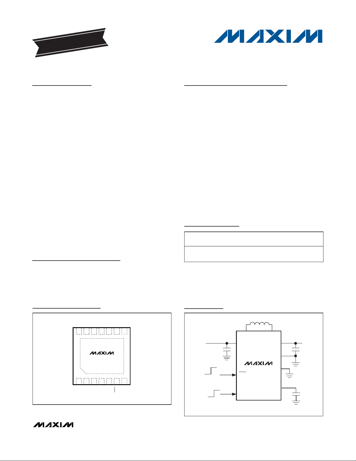
Ordering Information
Typical Operating Circuit
19-1006; Rev 1; 5/08
*
US Patent #7,289,119.
True Shutdown is a trademark of Maxim Integrated Products, Inc.
EVALUATION KIT
AVAILABLE
Note: The device is specified over the -40°C to +85°C extended
temperature range.
+
Denotes a lead-free package.
**
EP = Exposed pad.
Pin Configuration
PART
MAX8625AETD+
PINPACKAGE
14 TDFN-EP**
(3mm x 3mm)
TOP MARK
ABQ
TOP VIEW
IN
GND
GNDLX2
MAX8625A
LX2
OUT
ON
OUTSKIP
REFFB
9
8
EP
6
7
INLX1
14
13 11 10
12
+
245
1
3
LX1
EP = EXPOSED PAD.
TDFN-EP
OFF
INPUT
2.7V TO 5.5V
PWM
SKIP
ON
LX1
IN
MAX8625A
SKIP
ON
LX2
OUT
GND
FB
REF
OUTPUT
3.3V
Page 2
MAX8625A
High-Efficiency, Seamless Transition,
Step-Up/Down DC-DC Converter
2 _______________________________________________________________________________________
ABSOLUTE MAXIMUM RATINGS
ELECTRICAL CHARACTERISTICS
(VIN= 3.6V, ON = SKIP = IN, FB = GND, V
OUT
= 3.3V, LX_ unconnected, C
REF
= C5 = 0.1µF to GND, Figure 4. TA= -40°C to +85°C.
Typical values are at T
A
= +25°C, unless otherwise noted.) (Note 2)
Stresses beyond those listed under “Absolute Maximum Ratings” may cause permanent damage to the device. These are stress ratings only, and functional
operation of the device at these or any other conditions beyond those indicated in the operational sections of the specifications is not implied. Exposure to
absolute maximum rating conditions for extended periods may affect device reliability.
IN, OUT, SKIP, ON to GND ......................................-0.3V to +6V
REF, FB, to GND...............................................-0.3V, (IN + 0.3V)
LX2, LX1 (Note 1).........................................................±1.5A
RMS
Continuous Power Dissipation (TA= +70°C)
Single-Layer Board (derate 18.5mW/°C
above T
A
= +70°C) ...................................................1482mW
Operating Temperature Range ...........................-40°C to +85°C
Junction Temperature......................................................+150°C
Storage Temperature Range .............................-65°C to +150°C
Lead Temperature (soldering, 10s) .................................+300°C
Note 1: LX1 and LX2 have internal clamp diodes to IN, PGND and OUT, PGND, respectively. Applications that forward bias these
diodes should take care not to exceed the device's power-dissipation limits.
PARAMETER SYMBOL CONDITIONS MIN TYP MAX UNITS
Supply Range V
UVLO Threshold UVLO VIN rising, 60mV hysteresis 2.20 2.49 V
Quiescent Supply Current, FPWM
Mode, Switching
Quiescent Supply Current, Skip
Mode, Switching
Quiescent Supply Current, No
Switching, Skip Mode
Shutdown Supply Current I
Output Voltage Accuracy
(Fixed Output)
Output Voltage Range
(Adjustable Output)
Maximum Output Current VIN = 3.6V 0.80 A
Soft-Start L = 3.3µH; C
Load Regulation I
Line Regulation VIN = 2.5V to 5.5V 0.03 %/V
OUT Bias Current I
REF Output Voltage V
REF Load Regulation I
FB Feedback Threshold V
IN
I
IN
I
IN
I
IN
IN
OUT
REF
FB
No load, V
SKIP = GND, no load 37 µA
SKIP = GND, FB = 1.3V 35 45 µA
ON = GND, TA = +25°C 0.1 1
TA = +85°C 0.2
PWM mode, VIN = 2.5V to 5.5V 3.30 V
I
OUT
T
A
SKIP mode, valley regulation value 3.28 V
Average skip voltage 3.285
Load step +0.5A -3 %
OUT
V
OUT
VIN = 2.5V to 5.5V 1.244 1.25 1.256 V
REF
I
OUT
to 5.5V
OUT
= 0 to 0.5A, VIN = 2.5V to 5.5V,
= -40°C to +85°C (Note 3)
= 0 to 500mA 0.1 %/mA
= 3.3V 3 µA
= 10µA 1 mV
= 0 to full load, PWM mode; VIN = 2.5V
2.5 5.5 V
= 3.2V 15 22 mA
-1 +1 %
1.25 4.00 V
= C3 + C4 = 44µF 250 mA/ms
OUT
1.244 1.25 1.258 V
µA
Page 3
MAX8625A
High-Efficiency, Seamless Transition,
Step-Up/Down DC-DC Converter
_______________________________________________________________________________________ 3
Note 2: Devices are production tested at TA= +25°C. Specifications over the operating temperature range are guaranteed by
design and characterization.
Note 3: Limits are guaranteed by design and not production tested.
Note 4: The idle-mode current threshold is the transition point between fixed-frequency PWM operation and idle-mode operation.
The specification is given in terms of output load current for an inductor value of 3.3µH. For the step-up mode, the idle-mode
transition varies with input to the output-voltage ratios.
ELECTRICAL CHARACTERISTICS (continued)
(VIN= 3.6V, ON = SKIP = IN, FB = GND, V
OUT
= 3.3V, LX_ unconnected, C
REF
= C5 = 0.1µF to GND, Figure 4. TA= -40°C to +85°C.
Typical values are at T
A
= +25°C, unless otherwise noted.) (Note 2)
PARAMETER SYMBOL CONDITIONS MIN TYP MAX UNITS
FB Dual-Mode Threshold V
FB Leakage Current I
ON, SKIP Input High Voltage V
ON, SKIP Input Low Voltage V
ON Input Leakage Current I
SKIP Input Leakage Current
Peak Current Limit I
Fault Latch-Off Delay 100 ms
MOSFET On-Resistance R
Rectifier-Off Current Threshold I
Idle-Mode Current Threshold
(Note 4)
LX1, LX2 Leakage Current I
Out Reverse Current I
Minimum T
OSC Frequency F
Thermal Shutdown 15°C hysteresis +165 °C
ON
T
FBDM
FB
IHL
I
SKIPH
I
SKIPL
LIMP
ON
LX1OFF
I
SKIP
LXLKG
LXLKGR
ONMIN
OSCPWM
VFB = 1.3V, TA = +25°C 0.001 0.1
VFB = 1.3V, TA = +85°C 0.01
2.5V < VIN < 5.5V 1.6 V
IH
2.5V < VIN < 5.5V 0.45 V
IL
2.5V < VIN < 5.5V, TA = +25°C 0.001 1
TA = +85°C 0.01
V
= 3.6V 3 12
SKIP
V
= 0V -2 -0.2
SKIP
LX1 PMOS 1700 2000 2300 mA
Each MOSFET, TA = +25°C 0.05 0.1
Each MOSFET, VIN = 2.5V to 5.5V,
T
= -40°C to +85°C
A
SKIP = GND 125 mA
SKIP = GND, load decreasing 100
Load increasing 300
VIN = V
V
= 0V to V
LX2
TA = +85°C 0.2
VIN = V
measure I (LX2), T
TA = +85°C 0.5
OUT
LX1
= V
= 5.5V, V
, TA = +25°C
OUT
= 0V, V
LX2
A
= 0V to VIN,
LX1
OUT
= +25°C
75 100 125 mV
0.2
0.01 1
= 5.5V,
850 1000 1150 kHz
0.01 1
25 %
µA
µA
µA
Ω
mA
µA
µA
Page 4
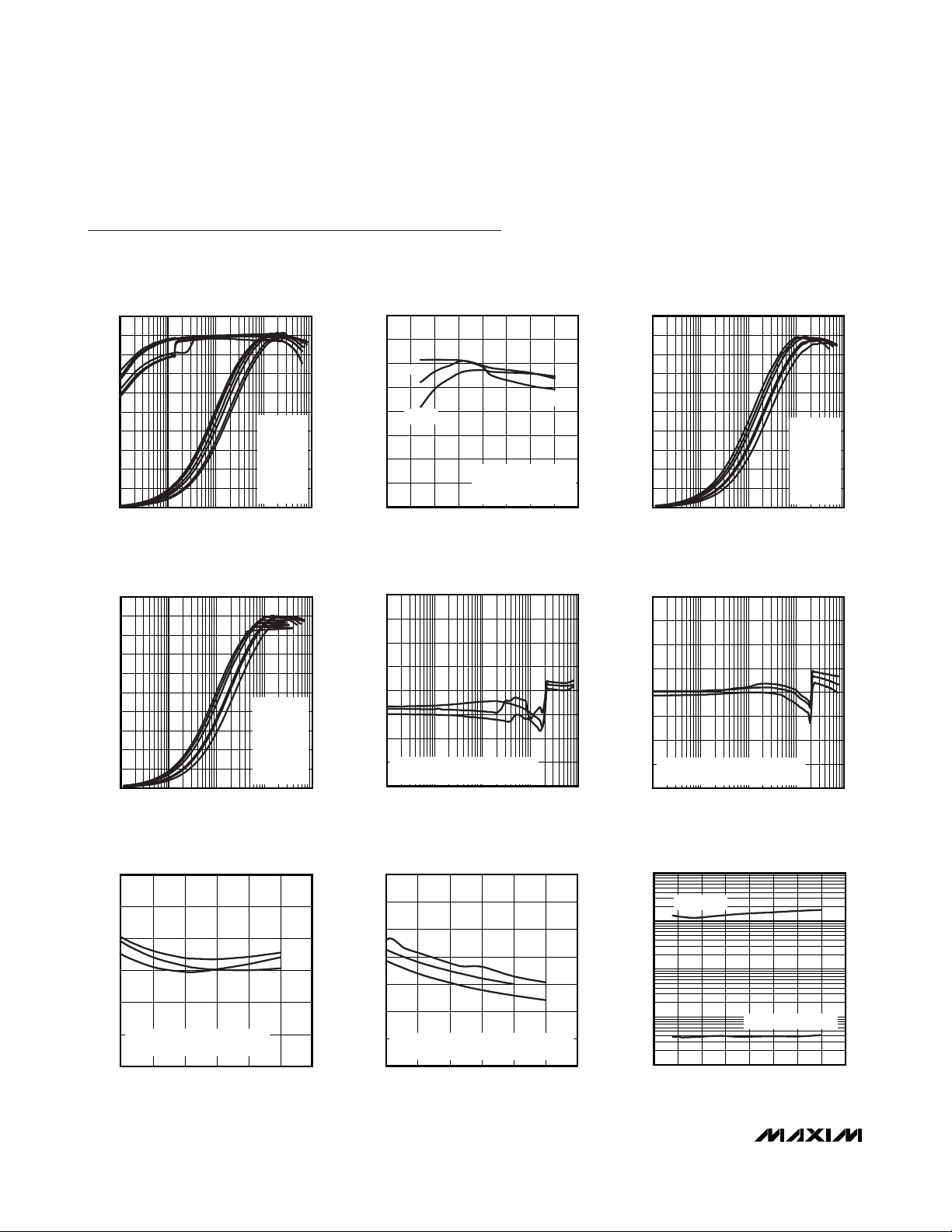
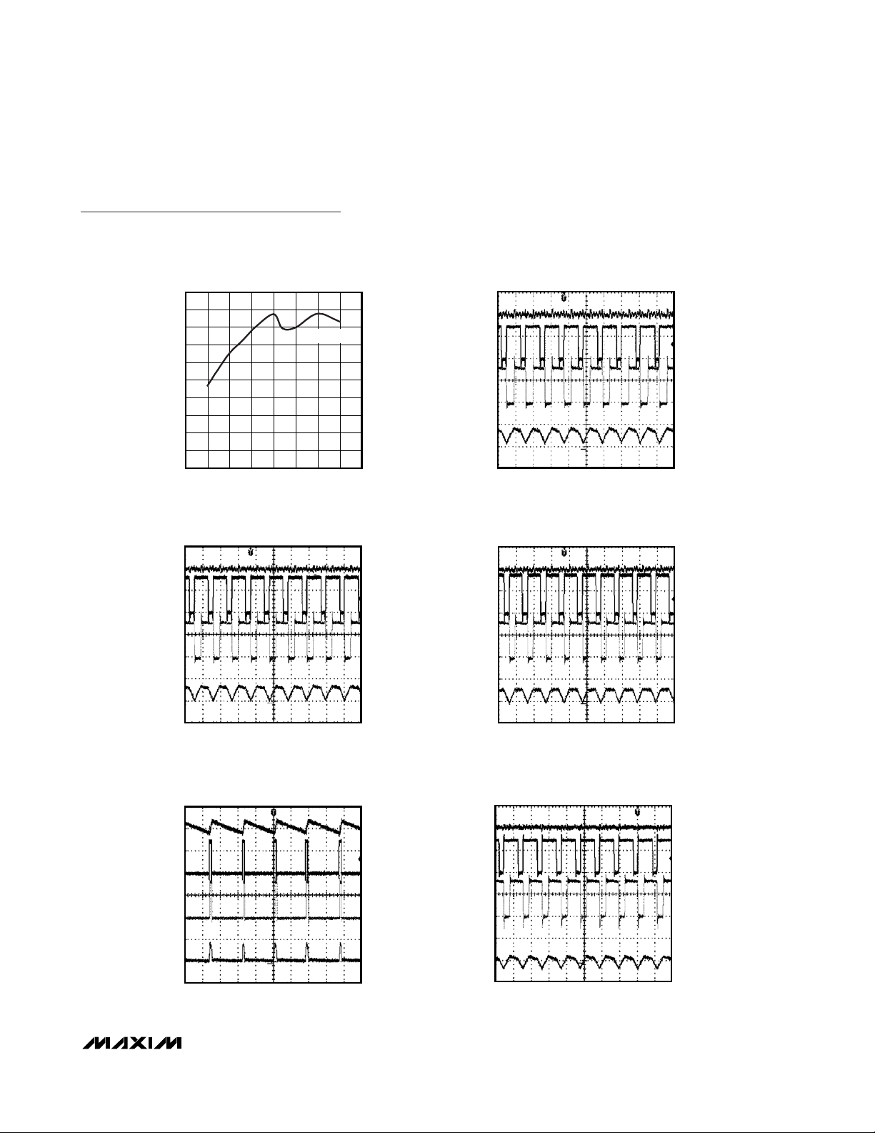
Typical Operating Characteristics
(VIN= 3.6V, SKIP = GND, TA= +25°C, Figure 4, unless otherwise noted.)
MAX8625A
High-Efficiency, Seamless Transition,
Step-Up/Down DC-DC Converter
4 _______________________________________________________________________________________
EFFICIENCY vs. LOAD CURRENT
SKIP AND FPWM MODES
100
90
80
70
60
50
40
EFFICIENCY (%)
30
20
10
0
0.1 1000
LOAD CURRENT (mA)
EFFICIENCY vs. LOAD CURRENT
FPWM MODE (FIGURE 3)
100
90
80
70
60
50
40
EFFICIENCY (%)
30
20
10
0
0.1 1000
LOAD CURRENT (mA)
SKIP-MODE EFFICIENCY
100
95
MAX8625A toc01
V
= 3.3V
OUT
= 2.7V
V
IN
3.0V,
3.3V,
3.6V,
4.2V,
5.0V
100101
90
85
80
75
EFFICIENCY (%)
70
65
60
2.0 3.0 3.52.5 4.0 4.5 5.0 5.5 6.0
vs. INPUT VOLTAGE
300mA
500mA
INPUT VOLTAGE (V)
100mA
V
= 3.3V
OUT
LOAD CURRENT = 100mA,
300mA, 500mA
MAX8625A toc02
EFFICIENCY (%)
OUTPUT VOLTAGE (3.3V INTERNAL FB)
vs. LOAD CURRENT
2.0
1.5
MAX8625A toc04
1.0
0.5
V
= 3.45V
OUT
= 2.7V
V
IN
3.0V,
3.3V,
3.6V,
4.2V,
5.0V
100101
0
DEVIATION (%)
-0.5
-1.0
-1.5
V
= 3.3V
OUT
= +25°C, TA = -40°C, TA = +85°C,
T
A
-2.0
0.1 1000
LOAD CURRENT (mA)
100101
MAX8625A toc05
DEVIATION (%)
EFFICIENCY vs. LOAD CURRENT
FPWM MODE (FIGURE 3)
100
90
80
70
60
50
40
30
20
10
0
0.1 1000
LOAD CURRENT (mA)
V
OUT
V
100101
OUTPUT VOLTAGE (2.8V EXTERNAL FB)
vs. LOAD CURRENT (FIGURE 3)
2.0
1.5
1.0
0.5
0
-0.5
-1.0
V
-1.5
-2.0
= 2.8V
OUT
= +25°C, TA = -40°C, TA = +85°C
T
A
0.1 1000
LOAD CURRENT (mA)
100101
= 2.8V
= 2.7V
IN
3.0V,
3.3V,
3.6V,
4.2V,
5.0V
MAX8625A toc03
MAX8625A toc06
OUTPUT VOLTAGE vs. INPUT VOLTAGE
WITH INTERNAL FB RESISTORS
3.33
3.32
3.31
3.30
3.29
OUTPUT VOLTAGE (V)
3.28
LOAD: 500mA, V
= +25°C, TA = -40°C, TA = +85°C
T
A
3.27
3.0 4.0 4.53.5 5.0 5.5 6.0
= 3.3V
OUT
INPUT VOLTAGE (V)
MAX8625A toc07
OUTPUT VOLTAGE (V)
OUTPUT VOLTAGE vs. INPUT VOLTAGE
WITH EXTERNAL FB RESISTORS
2.82
2.81
2.80
2.79
2.78
2.77
2.76
LOAD: 500mA, V
= +25°C, TA = -40°C, TA = +85°C (FIGURE 3)
T
A
2.75
3.0 4.0 4.53.5 5.0 5.5 6.0
= 2.8V
OUT
INPUT VOLTAGE (V)
MAX8625A toc08
SUPPLY CURRENT vs. INPUT VOLTAGE
WITH NO LOAD
100
FPWM MODE
10
1
SUPPLY CURRENT (mA)
0.1
0.01
2.0 6.0
INPUT VOLTAGE (V)
NO LOAD V
OUT
MAX8625A toc09
= 3.3V
5.55.04.54.03.53.02.5
Page 5
Typical Operating Characteristics (continued)
(VIN= 3.6V, SKIP = GND, TA= +25°C, Figure 4, unless otherwise noted.)
MAX8625A
High-Efficiency, Seamless Transition,
Step-Up/Down DC-DC Converter
_______________________________________________________________________________________
5
MAXIMUM LOAD CURRENT
1000
900
800
700
600
500
400
300
MAXIMUM LOAD CURRENT (mA)
200
100
0
2.0 3.0 3.52.5 4.0 4.5 5.0 5.5 6.0
V
V
LX1
2V/div
vs. INPUT VOLTAGE
INPUT VOLTAGE (V)
SWITCHING WAVEFORMS
= 3.3V, LOAD = 500mA, V
IN
V
OUT
= 3.3V
= 3.3V
OUT
MAX8625A toc12
MAX8625A toc10
V
OUT
50mV/div
(AC-COUPLED)
SWITCHING WAVEFORMS
= 3V, LOAD = 500mA, V
V
IN
V
LX1
2V/div
V
LX2
2V/div
SWITCHING WAVEFORMS
= 3.6V, LOAD = 500mA, V
V
IN
V
LX1
2V/div
1
μs/div
OUT
MAX8625A toc11
OUT
MAX8625A toc13
= 3.3V
= 3.3V
V
OUT
50mV/div
(AC-COUPLED)
I
LX
500mA/div
V
OUT
50mV/div
(AC-COUPLED)
CH1 = V
CH2 = V
V
2V/div
2V/div
2V/div
LX2
I
LX
500mA/div
1
μs/div
SKIP MODE
= 3V, LOAD = 20mA,
V
IN
= 3.288V
V
OUT
LX1
LX2
10μs/div
MAX8625A toc14
V
OUT
20mV/div
(AC-COUPLED)
I
LX
500mA/div
V
2V/div
V
2V/div
V
2V/div
LX2
I
LX
500mA/div
1
μs/div
FPWM MODE
= 3V, LOAD = 20mA,
V
IN
= 3.308V
V
OUT
LX1
LX2
1μs/div
MAX8625A toc15
OUT
20mV/div
(AC-COUPLED)
I
LX
500mA/div
Page 6

MAX8625A
High-Efficiency, Seamless Transition,
Step-Up/Down DC-DC Converter
6 _______________________________________________________________________________________
Typical Operating Characteristics (continued)
(VIN= 3.6V, SKIP = GND, TA= +25°C, Figure 4, unless otherwise noted.)
1ms/div
LINE TRANSIENT
V
OUT
= 3.3V, LOAD = 5.5Ω,
V
IN
RAMP 3V TO 4V
MAX8625A toc19
CH1 = V
IN
500mV/div
3V OFFSET
CH2 = V
OUT
50mV/div
(AC-COUPLED)
BODE PLOT
GAIN AND PHASE vs. FREQUENCY
MAX8625A toc20
FREQUENCY (kHz)
GAIN (dB)
10010
-50
-40
-30
-20
-10
0
10
20
30
40
-60
1 1000
VIN = 3.6
V
OUT
= 3.3V
LOAD = 200mA
-180
-144
-108
-72
-36
0
36
72
108
144
180
PHASE (DEG)
GAIN
PHASE
0.90
0.94
0.92
0.98
0.96
1.04
1.02
1.00
1.06
-40 0-20 20 40 60 80 100
OSCILLATOR FREQUENCY
vs. TEMPERATURE
MAX8625A toc21
TEMPERATURE (°C)
OSCILLATOR FREQUENCY (MHz)
= 3.6V, LOAD = 5Ω, V
V
IN
SHDN
2V/div
I
BATT
500mA/div
STARTUP WAVEFORMS
OUT
2ms/div
LOAD TRANSIENT
= 3.3V
V
OUT
= 3.288V
MAX8625A toc16
MAX8625A toc18
V
OUT
20mV/div
I
LX
500mA/div
V
OUT
100mV/div
(DC OFFSET = 3.3V)
I
BATT
250mA/div
SHDN
2V/div
V
OUT
500mA/div
STARTUP WAVEFORMS (FIGURE 3)
= 3.6V, LOAD = 30Ω, V
V
IN
2ms/div
OUT
MAX8625A toc17
= 1.5V
I
LX
500mA/div
I
BATT
100mA/div
I
LX
500mA/div
400
μs/div
Page 7

MAX8625A
High-Efficiency, Seamless Transition,
Step-Up/Down DC-DC Converter
_______________________________________________________________________________________
7
Typical Operating Characteristics (continued)
(VIN= 3.6V, SKIP = GND, TA= +25°C, Figure 4, unless otherwise noted.)
2.28
2.34
2.32
2.30
2.36
2.38
2.40
2.42
2.44
2.46
2.48
-50 0-25 25 50 75 100
MINIMUM STARTUP VOLTAGE
vs. TEMPERATURE
MAX8625A toc22
TEMPERATURE (°C)
MINIMUM STARTUP VOLTAGE (V)
V
OUT
= 3.3V, NO LOAD
1.22
1.24
1.23
1.26
1.25
1.27
1.28
-40 20 40-20 0 60 80 100
REFERENCE vs. TEMPERATURE
NO LOAD
MAX8625A toc23
TEMPERATURE (°C)
REFERENCE (V)
V
OUT
= 3.3V
V
IN
= 3.0V,
3.6V,
4.2V,
5.0V
1.22
1.24
1.23
1.26
1.25
1.27
1.28
-40 20 40-20 0 60 80 100
REFERENCE vs. TEMPERATURE
WITH 300mA LOAD
MAX8625A toc24
TEMPERATURE (°C)
REFERENCE (V)
V
OUT
= 3.3V
V
IN
= 3.0V,
3.6V,
4.2V,
5.0V
100
μs/div
SHUTDOWN DUE TO OVERLOAD
V
IN
= 3.6V, V
OUT
= 3.288V
MAX8625A toc25
V
LX2
2V/div
V
LX2
2V/div
V
OUT
500mV/div
I
LX
500mA/div
2μs/div
BOOST-TO-BUCK TRANSITION
FPWM MODE V
IN
= 3.6V, V
OUT
= 3.288V
MAX8625A toc26
V
IN
1V/div
DC OFFSET = 3V
V
OUT
100mV/div
AC-COUPLED
I
LX
200mA/div
Page 8

MAX8625A
High-Efficiency, Seamless Transition,
Step-Up/Down DC-DC Converter
8 _______________________________________________________________________________________
Detailed Description
The MAX8625A step-up/down architecture employs a
true H-bridge topology that combines a boost converter
and a buck converter topology using a single inductor
and output capacitor (Figure 1). The MAX8625A utilizes
a pulse-width modulated (PWM), current-mode control
scheme and operates at a 1MHz fixed frequency to
minimize external component size. A proprietary
H-bridge design eliminates mode changes when transitioning from buck to boost operation. This control
scheme provides very low output ripple using a much
smaller inductor than a conventional H-bridge, while
avoiding glitches that are commonly seen during mode
transitions with competing devices.
The MAX8625A switches at an internally set frequency
of 1MHz, allowing for tiny external components. Internal
compensation further reduces the external component
count in cost- and space-sensitive applications. The
MAX8625A is optimized for use in HDDs, DSCs, and
other devices requiring low-quiescent current for optimal light-load efficiency and maximum battery life.
Control Scheme
The MAX8625A basic noninverting step-up/down converter operates with four internal switches. The control
logic determines which two internal MOSFETs operate
to maintain the regulated output voltage. Unlike a traditional H-bridge, the MAX8625A utilizes smaller peakinductor currents, thus improving efficiency and
lowering input/output ripple.
The MAX8625A uses three operating phases during
each switching cycle. In phase 1 (fast-charge), the
inductor current ramps up with a di/dt of VIN/L. In phase
2 (slow charge/discharge), the current either ramps up
or down depending on the difference between the input
voltage and the output voltage (VIN- V
OUT
)/L. In phase 3
(discharge), the inductor current discharges at a rate of
V
OUT
/L through MOSFETs P2 and N1 (see Figure 1). An
additional fourth phase (phase 4: hold) is entered when
the inductor current falls to zero during phase 3. This
fourth phase is only used during skip operation.
The state machine (Figure 2) decides which phase to
use and when to switch phases. The converter goes
through the first three phases in the same order at all
Pin Description
PIN NAME FUNCTION
1, 2 LX1
3, 4 LX2
5 ON Enable Input. Connect ON to the input or drive high to enable the IC. Drive ON low to disable the IC.
6 SKIP
7FB
Inductor Connection 1. Connect the inductor between LX1 and LX2. Both LX1 pins must be connected
together externally. LX1 is internally connected to GND during shutdown.
Inductor Connection 2. Connect the inductor between LX1 and LX2. Both LX2 pins must be connected
together externally. LX2 is internally connected to GND during shutdown.
Mode Select Input. Connect SKIP to GND to enable skip mode. This mode provides the best overall
efficiency curve.
Connect SKIP to IN to enable forced-PWM mode. This mode provides the lowest noise, but reduces lightload efficiency compared to skip mode.
Feedback Input. Connect to ground to set the fixed 3.3V output. Connect FB to the center tap of an
external resistor-divider from the output to GND to set the output voltage to a different value. VFB regulates
to 1.25V.
8 REF
9, 10 OUT
11, 12 GND Ground. Connect the exposed pad and GND directly under the IC.
13, 14 IN
—EP
Reference Output. Bypass REF to GND with a 0.1µF ceramic capacitor. V
pulled to GND during shutdown.
Power Output. Bypass OUT to GND with two 22µF ceramic capacitors. Both OUT pins must be connected
together externally.
Power-Supply Input. Bypass IN to GND with two 22µF ceramic capacitors. Connect IN to a 2.5V to 5.5V
supply. Both IN pins must be connected together externally.
Exposed Pad. Connect to GND directly under the IC. Connect to a large ground plane for increased
thermal performance.
is 1.25V and is internally
REF
Page 9

MAX8625A
High-Efficiency, Seamless Transition,
Step-Up/Down DC-DC Converter
_______________________________________________________________________________________ 9
times. This reduces the ripple and removes any mode
transitions from boost-only or buck-only to hybrid modes
as seen in competing H-bridge converters.
The time spent in each phase is set by a PWM controller, using timers and/or peak-current regulation on a
cycle-by-cycle basis. The heart of the PWM control
block is a comparator that compares the output voltage-error feedback signal and the sum of the currentsense and slope compensation signals. The currentmode control logic regulates the inductor current as a
function of the output error voltage signal. The currentsense signal is monitored across the MOSFETs (P1, N1,
and N2). A fixed time delay of approximately 30ns
occurs between turning the P1 and N2 MOSFETs off,
and turning the N1 and P2 MOSFETs on. This dead
time prevents efficiency loss by preventing “shootthrough” current.
Step-Down Operation (V
IN
> V
OUT
)
During medium and heavy loads and V
IN
> V
OUT
,
MOSFETs P1 and N2 turn on to begin phase 1 at the
clock edge and ramp up the inductor current. The
duration of phase 1 is set by an internal timer. During
phase 2, N2 turns off, and P2 turns on to further ramp
up inductor current and also transfer charge to the output. This slow charge phase is terminated on a clock
edge and P1 is turned off. The converter now enters the
fast discharge phase (phase 3). In phase 3, N1 turns
on and the inductor current ramps down to the valley
current-regulation point set by the error signal. At the
end of phase 3, both P2 and N1 turn off and another
phase 1 is initiated and the cycle repeats.
With SKIP asserted low, during light loads when inductor current falls to zero in phase 3, the converter switches to phase 4 to reduce power consumption and avoid
Figure 1. Simplified Block Diagram
IN
P1 P2
LX1 LX2
OUT
ON
SKIP
REF
GND
UVLO
REFERENCE
MAX8625
P1
CURRENT SENSE
1.25V
125mV
Gm
N1
PWM/PFM
CONTROL
N2
OSCILLATOR
FB
Page 10

MAX8625A
High-Efficiency, Seamless Transition,
Step-Up/Down DC-DC Converter
10 ______________________________________________________________________________________
shuttling current in and out of the output capacitor. If
SKIP is asserted high for forced-PWM mode, phase 4 is
not entered and current shuttling is allowed (and is
necessary to maintain the PWM operation frequency
when no load is present).
Step-Up Operation (V
IN
< V
OUT
)
During medium and heavy loads when V
IN
< V
OUT,
MOSFETs P1 and N2 turn on at the clock edge to ramp
up the inductor current. Phase 1 terminates when the
inductor current reaches the peak target current set by
the PWM comparator and N2 turns off. This is followed
by a slow-discharge phase (phase 2) instead of a
charge phase (since VINis less than V
OUT
) when P2
turns on. The slow-discharge phase terminates on a
clock edge. The converter now enters the fast-discharge phase (phase 3). During phase 3, P1 turns off
and N1 turns on. At the end of the minimum time, both
P2 and N1 turn off and the cycle repeats.
If SKIP is asserted low, during light loads when inductor
current falls to zero in phase 3, the converter switches to
phase 4 (hold) to reduce power consumption and avoid
shuttling current in and out of the output. If SKIP is high
to assert forced-PWM mode, the converter never enters
phase 4 and allows negative inductor current.
Step-Up/Down Transition-Zone Operation
(V
IN
= V
OUT
)
When V
IN
= V
OUT
, the converter still goes through the
three phases for moderate to heavy loads. However,
the maximum time is now spent in phase 2 where
inductor current di/dt is almost zero, since it is proportional to (VIN- V
OUT
). This eliminates transition glitches
Figure 2. State Diagram
FAULT
TIMEOUT
(ASYNCHRONOUS
FROM ANYWHERE)
ERROR
ON = 1
P1, P2 = OFF
N1, N2 = ON
PHASE 2
SLOW CHARGE/
DISCHARGE
OSC = ON
P1, P2 = ON
N1, N2 = OFF
T2-3
PHASE 3
FAST DISCHARGE
OSC = ON
P2, N1 = ON
P1, N2 = OFF
ON = 1, P1, P2 = OFF, N1, N2 = ON,
POWER-UP
OSC = ON AND REF = ON IF UVLO OK
T1-2
T1-3
T3-1
T3-4
(SKIP)
OFF
ON = 0
P1, P2 = OFF
N1, N2 = ON
= 0μA
I
Q
TRUN
PHASE 1
FAST-CHARGE
OSC = ON
P1, N2 = ON
P2, N1 = OFF
T4-1
PHASE 4
HOLD
OSC = OFF
N1, N2 = ON
P1, P2 = OFF
ON = 0
(ASYNCHRONOUS
FROM
ANYWHERE)
TPUP
REFOK = 0 OR
UVLO = 0
(ASYNCHRONOUS
FROM ANYWHERE)
Page 11

MAX8625A
High-Efficiency, Seamless Transition,
Step-Up/Down DC-DC Converter
______________________________________________________________________________________ 11
or oscillation between the boost and buck modes as
seen in other step-up/down converters. See the switching waveforms for each of the three modes and transition waveforms in the
Typical Operating Characteristics
section.
Forced-PWM Mode
Drive SKIP high to operate the MAX8625A in forcedPWM mode. In this mode, the IC operates at a constant
1MHz switching frequency with no pulse skipping. This
scheme is desirable in noise-sensitive applications
because the output ripple is minimized and has a predictable noise spectrum. Forced PWM consumes higher
supply current at light loads due to constant switching.
Skip Mode
Drive SKIP low to operate the MAX8625A in skip mode
to improve light-load efficiency. In skip mode, the IC
switches only as necessary to maintain the output at
light loads, but still operates with fixed-frequency PWM
at medium and heavy loads. This maximizes light-load
efficiency and reduces the input quiescent current to
37µA (typ).
Load Regulation and Transient Response
During a load transient, the output voltage instantly
changes due to the ESR of the output capacitors by an
amount equal to their ESR times the change in load
current (ΔV
OUT
= R
ESR
x ΔI
LOAD
). The output voltage
then deviates further based on the speed at which the
loop compensates for the load step. Increasing the output capacitance reduces the output-voltage droop. See
the
Capacitor Selection
section. The typical application
circuit limits the output transient droop to less than 3%.
See the
Typical Operating Characteristics
section.
Soft-Start
Soft-start prevents input inrush current during startup.
Internal soft-start circuitry ramps the peak inductor current with an internal DAC in 8ms. Once the output
reaches regulation, the current limit immediately jumps
to the maximum threshold. This allows full load capability as soon as regulation is reached, even if it occurs
before the 8ms soft-start time is complete.
Shutdown
Drive ON low to place the MAX8625A in shutdown
mode and reduce supply current to less than 1µA.
During shutdown, OUT is disconnected from IN, and
LX1 and LX2 are connected to GND. Drive ON high for
normal operation.
Fault and Thermal Shutdown
The MAX8625A contains current-limit and thermal shutdown circuitry to protect the IC from fault conditions.
When the inductor current exceeds the current limit (2A
for the MAX8625A), the converter immediately enters
phase 3 and an internal 100ms timer starts. The converter continues to commutate through the three phases, spending most of its time in phase 1 and phase 3. If
the overcurrent event continues and the output is out of
regulation for the duration of the 100ms timer, the IC
enters shutdown mode and the output latches off. ON
must then be toggled to clear the fault. If the overload
is removed before the 100ms timer expires, the timer is
cleared and the converter resumes normal operation.
The thermal-shutdown circuitry disables the IC switching if the die temperature exceeds +165°C. The IC
begins soft-start once the die temperature cools by
15°C.
Page 12

MAX8625A
High-Efficiency, Seamless Transition,
Step-Up/Down DC-DC Converter
12 ______________________________________________________________________________________
Applications Information
Selecting the Output Voltage
The MAX8625A output is nominally fixed at 3.3V.
Connect FB to GND to select the internally fixed-output
voltage. For an adjustable output voltage, connect FB
to the center tap of an external resistor-divider connected from the output to GND (R1 and R2 in Figure 3).
Select 100kΩ for R2 and calculate R1 using the following equation:
where VFB= 1.25V and V
OUT
is the desired output reg-
ulation voltage. V
OUT
must be between 1.25V and 4V.
Note that the minimum output voltage is limited by the
minimum duty cycle. V
OUT
cannot be below 1.25V.
Calculating Maximum Output Current
The maximum output current provided by the MAX8625A
circuit depends on the inductor value, switching frequency, efficiency, and input/output voltage.
See the
Typical Operating Characteristics
section for
the Maximum Load Current vs. Input Voltage graph.
Capacitor Selection
The input and output ripple currents are both discontinuous in this topology. Therefore, select at least two
22µF ceramic capacitors at the input. Select two 22µF
ceramic output capacitors. For best stability over a
wide temperature range, use X5R or better dielectric.
Inductor Selection
The recommended inductance range for the
MAX8625A is 3.3µH to 4.7µH. Larger values of L give a
smaller ripple, while smaller L values provide a better
transient response. This is because, for boost and stepup/down topologies, the crossover frequency is
inversely proportional to the value of L for a given load
and input voltage. The MAX8625A is internally compensated, and therefore, the choice of power components
for stable operation is bounded. A 3.3µH inductor with
2A rating is recommended for the 3.3V fixed output with
0.8A load.
PCB Layout and Routing
Good PCB layout is important to achieve optimal performance from the MAX8625A. Poor design can cause
excessive conducted and/or radiated noise.
Conductors carrying discontinuous currents and any
high-current path should be made as short and wide as
possible. Keep the feedback network (R1 and R2) very
close to the IC, preferably within 0.2 inches of the FB
and GND pins. Nodes with high dv/dt (switching
nodes) should be kept as small as possible and routed
away from FB. Connect the input and output capacitors
as close as possible to the IC. Refer to the MAX8625A
evaluation kit for a PCB layout example.
Figure 3. Typical Application Circuit (Adjustable Output)
Rk
1 100 1 =× −
⎛
V
Ω
OUT
⎜
V
⎝
FB
⎞
⎟
⎠
L
3.3μH
12
INPUT
2.7V TO 5.5V
C1, C2
22μF
MODE
SELECTION
INPUT
OFF
0.1μF
ON
C5
13
IN
14
IN
6
SKIP
5
ON
8
REF
34
LX1LX1 LX2
U1
MAX8625A
LX2
OUT
OUT
GND
GND
9
10
R1
140kΩ
7
FB
R2
100kΩ
11
12
OUTPUT
C3, C4
22μF
3V
Page 13

MAX8625A
High-Efficiency, Seamless Transition,
Step-Up/Down DC-DC Converter
______________________________________________________________________________________ 13
Chip Information
PROCESS: BiCMOS
Figure 4. Typical Application Circuit (Fixed 3.3V Output)
Package Information
For the latest package outline information and land patterns, go
to www.maxim-ic.com/packages
.
PACKAGE TYPE PACKAGE CODE DOCUMENT NO.
14 TDFN-EP T1433-2
21-0137
12
INPUT
2.7V TO 5.5V
C1, C2
22μF
MODE
SELECTION
INPUT
OFF
ON
C5
0.1μF
13
IN
14
IN
6
SKIP
5
ON
8
REF
L
3.3μH
34
LX1LX1 LX2
U1
MAX8625A
LX2
OUT
OUT
GND
GND
9
10
7
FB
11
12
OUTPUT
3.3V
C3, C4
22μF
Page 14
MAX8625A
High-Efficiency, Seamless Transition,
Step-Up/Down DC-DC Converter
Maxim cannot assume responsibility for use of any circuitry other than circuitry entirely embodied in a Maxim product. No circuit patent licenses are
implied. Maxim reserves the right to change the circuitry and specifications without notice at any time.
14
____________________Maxim Integrated Products, 120 San Gabriel Drive, Sunnyvale, CA 94086 408-737-7600
© 2008 Maxim Integrated Products Printed USA is a registered trademark of Maxim Integrated Products. Inc.
Revision History
REVISION
NUMBER
0 3/08 Initial release —
1 5/08 Added PCB Layout and Routing section 12
REVISION
DATE
DESCRIPTION
PAGES
CHANGED
 Loading...