

Page 1
General Description
The MAX8621Y/MAX8621Z power-management integrated circuits (PMICs) are designed for a variety of
portable devices including cellular handsets. These
PMICs include two high-efficiency step-down DC-DC
converters, four low-dropout linear regulators (LDOs)
with pin-programmable capability, one open-drain driver, a 60ms (typ) reset timer, and power-on/off control
logic. These devices offer high efficiency with a no-load
supply current of 160µA, and their small thin QFN 4mm
x 4mm package makes them ideal for portable devices.
The step-down DC-DC converters utilize a proprietary
4MHz hysteretic-PWM control scheme that allows for
ultra-small external components. Internal synchronous
rectification improves efficiency and eliminates the
external Schottky diode that is required in conventional
step-down converters. The output voltage is adjustable
from 0.6V to 3.3V. The output current is guaranteed up
to 500mA.
The four LDOs offer low 45µV
RMS
output noise and low
dropout of only 100mV at 100mA. OUT1 and OUT2
deliver 300mA (min) of continuous output current.
OUT3 and OUT4 deliver 150mA (min) of continuous
output current. The output voltages are pin selectable
by SEL1 and SEL2 for flexibility. The MAX8621Y/
MAX8621Z offer different sets of LDO output voltages.
A microprocessor reset output (RESET) monitors OUT1
and warns the system of impending power loss, allowing safe shutdown. RESET asserts during power-up,
power-down, shutdown, and fault conditions where
V
OUT1
is below its regulation voltage.
A 200mA driver output is provided to control LED backlighting or provide an open-drain connection for resistors such as in feedback networks.
Applications
Cellular Handsets
Smart Phones, PDAs
Digital Cameras
MP3 Players
Wireless LAN
Features
♦ Two 500mA Step-Down Converters
Up to 4MHz Switching Frequency
Adjustable Output from 0.6V to 3.3V
♦ Four Low-Noise LDOs with Pin-Programmable
Output Voltages
♦ One Open-Drain Driver
♦ 60ms (typ) Reset Timer
♦ Power-On/Off Control Logic and Sequencing
♦ 4mm x 4mm x 0.8mm 24-Pin Thin QFN
MAX8621Y/MAX8621Z
Dual Step-Down DC-DC Power-Management ICs
for Portable Devices
________________________________________________________________ Maxim Integrated Products 1
Ordering Information
MAX8621Y
MAX8621Z
IN1
IN2
IN3
PWRON
EN3
EN4
SEL2
ENDR
REFBP
GND
OUT1
OUT2
OUT3
OUT4
DR
LX1
FB1
PGND1
LX2
FB2
PGND2
RESET
SEL1
EN2
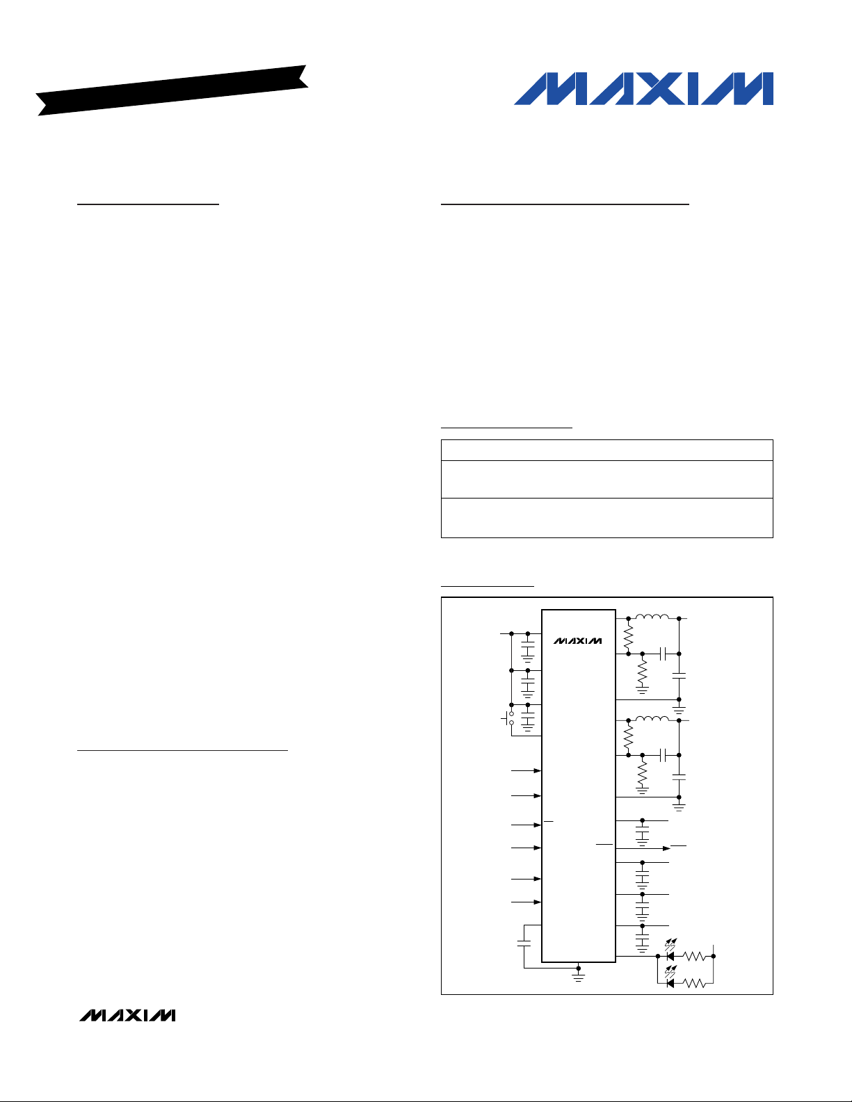
INPUT
2.6V TO 5.5V
INPUT
OUT4
3V, 150mA
OUT3
1.8V, 150mA
OUT2
2.6V, 300mA
OUT1
2.6V, 300mA
BUCK1
1.375V, 500mA
BUCK2
1.8V, 500mA
RESET
Typical Operating Circuit
19-3539; Rev 0; 1/05
For pricing, delivery, and ordering information, please contact Maxim/Dallas Direct! at
1-888-629-4642, or visit Maxim’s website at www.maxim-ic.com.
Pin Configuration appears at end of data sheet.
EVALUATION KIT AVAILABLE
PART TEMP RANGE PIN-PACKAGE
MAX8621YETG -40°C to +85°C
MAX8621ZETG -40°C to +85°C
24 Thin QFN
4mm x 4mm (T2444-4)
24 Thin QFN
4mm x 4mm (T2444-4)
Page 2
MAX8621Y/MAX8621Z
Dual Step-Down DC-DC Power-Management ICs
for Portable Devices
2 _______________________________________________________________________________________
ABSOLUTE MAXIMUM RATINGS
ELECTRICAL CHARACTERISTICS
(VIN= 3.7V, C
IN1
= 10µF, C
IN2
= C
IN3
= 4.7µF, C
OUT1
= C
OUT2
= 4.7µF, C
OUT3
= C
OUT4
= 2.2µF, C
REFBP
= 0.01µF, TA= -40°C to
+85°C, unless otherwise noted. Typical values are at T
A
= +25°C.) (Notes 1, 2)
Stresses beyond those listed under “Absolute Maximum Ratings” may cause permanent damage to the device. These are stress ratings only, and functional
operation of the device at these or any other conditions beyond those indicated in the operational sections of the specifications is not implied. Exposure to
absolute maximum rating conditions for extended periods may affect device reliability.
Note 1: LX_ has internal clamp diodes to GND and IN1. Applications that forward-bias these diodes should take care not to exceed
the IC’s package dissipation limits.
PWRON, IN1, IN2, IN3, RESET, FB1, FB2,
ENDR, REFBP, SEL1, SEL2 to GND..................-0.3V to +6.0V
EN2, EN3, EN4, DR to GND.......................-0.3V to (V
IN3
+ 0.3V)
OUT1, OUT2, OUT3, OUT4 to GND...........-0.3V to (V
IN2
+ 0.3V)
PGND1, PGND2 to GND ......................................-0.3V to + 0.3V
LX1, LX2 Current..........................................................±1.5A
RMS
LX1, LX2 to GND (Note 1) ..........................-0.3V to (V
IN1
+ 0.3V)
DR Current......................................................................0.5A
RMS
Continuous Power Dissipation (TA= +70°C)
24-Pin 4mm x 4mm Thin QFN
(derate 27.8mW/°C above +70°C)..........................2222.2mW
Operating Temperature Range ...........................-40°C to +85°C
Junction Temperature......................................................+150°C
Storage Temperature Range .............................-65°C to +150°C
Lead Temperature (soldering, 10s) .................................+300°C
PARAMETER CONDITIONS
MIN
TYP
MAX
UNIT
Input Supply Range After startup 2.6 5.5 V
Shutdown Supply Current V
IN
= 4.2V (Note 3) 2 15 µA
VIN = 3.7V; BUCK1, BUCK2, OUT1, OUT2 on; other
circuits off
300
No-Load Supply Current
VIN = 3.7V, BUCK1 and BUCK2 on, all LDOs on
µA
Light-Load Supply Current
V
IN
= 3.7V, BUCK1 and BUCK2 with 500µA load each,
OUT1 and OUT2 on, other circuits off
µA
UNDERVOLTAGE LOCKOUT
VIN rising
Undervoltage Lockout (Note 4)
V
IN
falling
V
THERMAL SHUTDOWN
Threshold TA rising
°C
Hysteresis 15 °C
REFERENCE
Reference Bypass Output
Voltage
T
A
= 0°C to +85°C
V
REF Supply Rejection 2.6V ≤ VIN ≤ 5.5V 0.2
mV/V
LOGIC AND CONTROL INPUTS
Input Low Level PWRON, EN2, EN3, EN4; 2.6V ≤ VIN ≤ 5.5V 0.4 V
PWRON, EN2, EN3, EN4; 2.6V ≤ VIN ≤ 4.2V
Input High Level
PWRON, EN2, EN3, EN4; 2.6V ≤ V
IN
≤ 5.5V
V
Logic Input Current EN3, EN4; 0V < VIN < 5.5V -1 +1 µA
Tristate Low Input Threshold SEL_ 0.3 0.7 1.0 V
Tristate Low Input Threshold
Hysteresis
SEL_ 50 mV
Tristate High Input Threshold SEL_
V
IN
-
VIN -
VIN -
V
160
2.35 2.55
+160
1.25
0.8V
275
710
2.70 2.85 3.05
1.235 1.250 1.265
1.44 1.12
1.2V
0.4V
Page 3
MAX8621Y/MAX8621Z
Dual Step-Down DC-DC Power-Management ICs
for Portable Devices
_______________________________________________________________________________________ 3
ELECTRICAL CHARACTERISTICS (continued)
(VIN= 3.7V, C
IN1
= 10µF, C
IN2
= C
IN3
= 4.7µF, C
OUT1
= C
OUT2
= 4.7µF, C
OUT3
= C
OUT4
= 2.2µF, C
REFBP
= 0.01µF, TA= -40°C to
+85°C, unless otherwise noted. Typical values are at T
A
= +25°C.) (Notes 1, 2)
PARAMETER CONDITIONS
UNIT
Tristate High Input Threshold
Hysteresis
SEL_ 50 mV
PWRON, EN2 Pulldown Resistor
to GND
kΩ
STEP-DOWN DC-DC CONVERTER 1 (BUCK1)
Supply Current I
LOAD
= 0A, no switching 40 µA
Output Voltage Range 0.6 3.3 V
FB1 Threshold Voltage V
FB1
falling
V
FB1 Threshold Line Regulation 2.6V ≤ VIN ≤ 5.5V 0.3 %/V
FB1 Threshold Voltage Hysteresis
(% of V
FB1
)
1%
Shutdown
FB1 Bias Current
V
FB1
= 0.5V
µA
p-MOSFET switch (I
LIMP
)
Current Limit
n-MOSFET rectifier (I
LIMN
)
mA
p-MOSFET switch, I
LX1
= -40mA
1.5
On-Resistance
n-MOSFET rectifier, I
LX1
= 40mA
0.8
Ω
Rectifier Off-Current Threshold I
LXOFF
45 70 mA
t
ON
Minimum On- and Off-Times
t
OFF
95
ns
STEP-DOWN DC-DC CONVERTER 2 (BUCK2)
Supply Current I
LOAD
= 0A, no switching 40 µA
Output Voltage Range 0.6 3.3 V
FB2 Threshold Voltage V
FB2
falling
V
FB2 Threshold Line Regulation 2.6V ≤ VIN ≤ 5.5V 0.3 %/V
FB2 Threshold Voltage Accuracy
(Falling) (% of VFB2)
I
LOAD
= 0A
%
FB2 Threshold Voltage Hysteresis
(% of VFB2)
1%
Shutdown
FB2 Bias Current
V
FB
= 0.5V
µA
p-MOSFET switch
Current Limit
n-MOSFET rectifier
mA
p-MOSFET switch, I
LX2
= -40mA
1.5
On-Resistance
n-MOSFET rectifier, I
LX2
= 40mA
0.8
Ω
Rectifier Off-Current Threshold I
LXOFF
45 70 mA
t
ON
Minimum On- and Off-Times
t
OFF
95
ns
MIN TYP MAX
400 800 1600
670 1000 1500
750 1000 1330
-2.5 +2.5
670 1000 1500
750 1000 1330
0.603
0.01
0.01
0.65
0.35
107
0.603
0.01
0.01
0.65
0.35
107
Page 4
MAX8621Y/MAX8621Z
Dual Step-Down DC-DC Power-Management ICs
for Portable Devices
4 _______________________________________________________________________________________
ELECTRICAL CHARACTERISTICS (continued)
(VIN= 3.7V, C
IN1
= 10µF, C
IN2
= C
IN3
= 4.7µF, C
OUT1
= C
OUT2
= 4.7µF, C
OUT3
= C
OUT4
= 2.2µF, C
REFBP
= 0.01µF, TA= -40°C to
+85°C, unless otherwise noted. Typical values are at T
A
= +25°C.) (Notes 1, 2)
PARAMETER CONDITIONS
UNIT
OUT1 (LDO1)
TA = 0°C to +85°C
I
LOAD
= 1mA, 3.7V ≤ VIN ≤ 5.5V,
relative to V
OUT(NOM)
Output Voltage Accuracy
I
LOAD
= 150mA, relative to V
OUT(NOM)
0
%
Output Current 300 mA
Current Limit V
OUT1
= 0V
940 mA
Dropout Voltage I
LOAD
= 200mA, TA = +85°C
420 mV
Load Regulation
V
IN
= greater of 3.7V or (V
OUT(NOM)
+ 0.7V),
1mA < I
LOAD
< 300mA, V
SEL1
= V
SEL2
= 0V
1.2 %
Power-Supply Rejection
∆V
OUT1
/∆V
IN2
10Hz to 10kHz, C
OUT1
= 4.7µF, I
LOAD
= 30mA 60 dB
Output Noise Voltage (RMS) 100Hz to 100kHz, C
OUT1
= 4.7µF, I
LOAD
= 30mA 45
µV
RMS
0 < I
LOAD
< 300mA 4.7
Output Capacitor for Stable
Operation
0 < I
LOAD
< 150mA 2.2
µF
Ground Current I
LOAD
= 500µA 21 µA
OUT2 (LDO2)
TA = 0°C to +85°C
I
LOAD
= 1mA, 3.7V ≤ V
IN_
≤ 5.5V,
relative to V
OUT(NOM)
Output Voltage Accuracy
I
LOAD
= 150mA, relative to V
OUT(NOM)
0
%
Output Current 300 mA
Current Limit V
OUT2
= 0V
940 mA
Dropout Voltage I
LOAD
= 200mA , T
A
= +85°C
420 mV
Load Regulation 1mA < I
LOAD
< 300mA, V
SEL1
= V
SEL2
= 0V 1.2 %
Power-Supply Rejection
∆V
OUT2
/∆V
IN2
10Hz to 10kHz, C
OUT2
= 4.7µF, I
LOAD
= 30mA 60 dB
Output Noise Voltage (RMS) 100Hz to 100kHz, C
OUT2
= 4.7µF, I
LOAD
= 30mA 45
µV
RMS
0 < I
LOAD
< 300mA 4.7
Output Capacitor for Stable
Operation
0 < I
LOAD
< 150mA 2.2
µF
Ground Current I
LOAD
= 500µA 21 µA
OUT3 (LDO3)
TA = 0°C to +85°C
I
LOAD
= 1mA, 3.7V ≤ V
IN_
≤ 5.5V,
relative to V
OUT(NOM)
Output Voltage Accuracy
I
LOAD
= 75mA, relative to V
OUT(NOM)
0
%
Output Current 150 mA
Current Limit V
OUT3
= 0V
650 mA
Dropout Voltage I
LOAD
= 100mA , TA = +85°C
210 mV
Load Regulation 1mA < I
LOAD
< 150mA, V
SEL1
= V
SEL2
= 0V 0.6 %
MIN TYP MAX
-1.3 +0.6 +2.0
TA = -40°C to +85°C -2.3 +2.5
310 550
TA = -40°C to +85°C -2.3 +2.5
TA = -40°C to +85°C -2.3 +2.5
-1.3 +0.6 +2.0
310 550
-1.3 +0.3 +2.0
165 360
200
200
100
Page 5
MAX8621Y/MAX8621Z
Dual Step-Down DC-DC Power-Management ICs
for Portable Devices
_______________________________________________________________________________________ 5
ELECTRICAL CHARACTERISTICS (continued)
(VIN= 3.7V, C
IN1
= 10µF, C
IN2
= C
IN3
= 4.7µF, C
OUT1
= C
OUT2
= 4.7µF, C
OUT3
= C
OUT4
= 2.2µF, C
REFBP
= 0.01µF, TA= -40°C to
+85°C, unless otherwise noted. Typical values are at T
A
= +25°C.) (Notes 1, 2)
PARAMETER CONDITIONS
UNIT
Power-Supply Rejection
∆V
OUT3
/∆V
IN2
10Hz to 10kHz, C
OUT3
= 2.2µF, I
LOAD
= 30mA 60 dB
Output Noise Voltage (RMS) 100Hz to 100kHz, C
OUT3
= 2.2µF, I
LOAD
= 30mA 45
µV
RMS
Output Capacitor for Stable
Operation
0 < I
LOAD
< 150mA 2.2 µF
OUT4 (LDO4)
)
TA = 0°C to
+85°C
)
I
LOAD
= 1mA, 3.7V ≤
V
IN_
≤ 5.5V, relative to
V
OUT(NOM)
TA = -40°C to +85°C
Output Voltage Accuracy
I
LOAD
= 75mA, relative to V
OUT(NOM)
0
%
Output Current 150 mA
Current Limit V
OUT4
= 0V
650 mA
Dropout Voltage I
LOAD
= 100mA, T
A
= +85°C
210 mV
Load Regulation 1mA < I
LOAD
< 150mA, V
SEL1
= V
SEL2
= 0 0.6 %
Power-Supply Rejection
∆V
OUT4
/∆V
IN2
10Hz to 10kHz, C
OUT4
= 2.2µF, I
LOAD
= 30mA 60 dB
Output Noise Voltage (RMS) 100Hz to 100kHz, C
OUT4
= 2.2µF, I
LOAD
= 30mA 45
µV
RMS
Output Capacitor for Stable
Operation
0 < I
LOAD
< 150mA 2.2 µF
DRIVER (DR)
ENDR Turn-On Threshold IDR = 1mA
V
ENDR Input Current V
ENDR
= 0V and 5.5V -1 +1 µA
DR Output Low Voltage IDR = 150mA, V
ENDR
= 3.7V 0.2 0.4 V
DR Off-Current (Leakage) VDR = VIN = 5.5V, V
ENDR
= 0V -1 +1 µA
RESET
Output High Voltage
V
OUT1
V
Output Low Voltage I
SINK
= 1mA 0.3 V
RESET Threshold Percentage of nominal OUT1 rising when RESET falls 84 87 90 %
RESET Active Timeout Period From OUT1 ≥ 87% until RESET = HIGH 60 ms
Pullup Resistance to OUT1 81420kΩ
Note 1: V
IN1
, V
IN2
, and V
IN3
are shorted together and single input is referred to as VIN.
Note 2: All units are 100% production tested at T
A
= +85°C. Limits over the operating range are guaranteed by design.
Note 3: OUT1, OUT2, OUT3, OUT4, LX1, and LX2 to ground.
Note 4: When the input voltage is greater than 2.85V (typ), the UVLO comparator trips and the threshold is reduced to 2.35V (typ).
This allows the system to start normally until the input voltage decays to 2.35V.
MIN TYP MAX
V
OUT(NOM
V
OUT(NOM
≥ 1.8V -1.3 +0.3 +2.0
= 1.5V -1.30 +0.3 +2.35
-2.3 +2.5
165 360
100
0.65
- 0.3V
Page 6
MAX8621Y/MAX8621Z
Dual Step-Down DC-DC Power-Management ICs
for Portable Devices
6 _______________________________________________________________________________________
Typical Operating Characteristics
(Circuit of Figure 3, V
IN1
= V
IN2
= V
IN3
= 3.6V, PWRON = IN, V
BUCK1
= 1.375V, V
BUCK2
= 1.8V, V
OUT1
= 2.6V, V
OUT2
= 2.6V, V
OUT3
= 1.8V, V
OUT4
= 3.0V, SEL1 = SEL2 = open, LX1 = LX2 = Murata LQH32CN2R2M53, TA= +25°C, unless otherwise noted.)
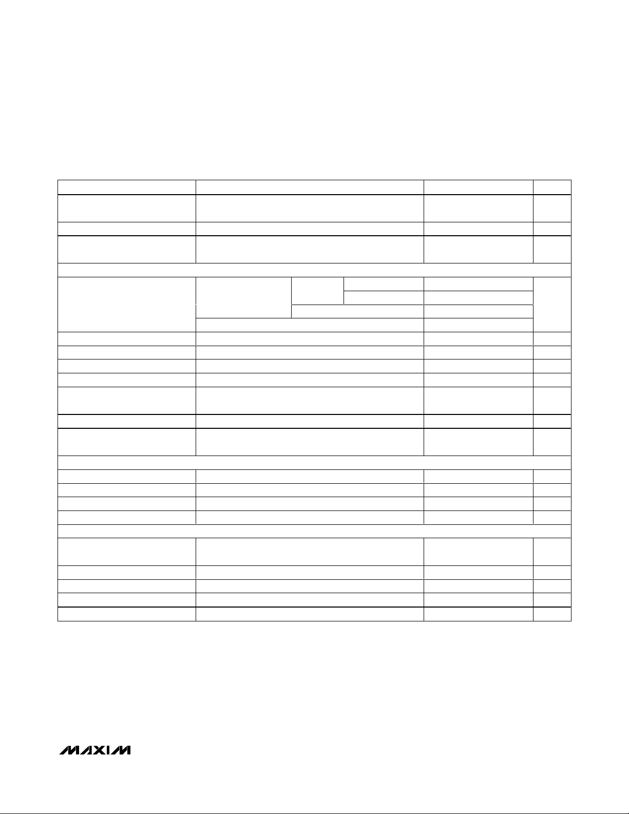
SUPPLY CURRENT
vs. INPUT VOLTAGE
MAX8621 toc01
INPUT VOLTAGE (V)
SUPPLY CURRENT (µA)
5.04.54.03.53.0
120
140
160
180
200
220
240
260
280
300
100
2.5 5.5
NO LOAD
BUCK1, BUCK2, OUT1, OUT2: ON
STARTUP WAVEFORMS
MAX8621 toc02
50µs/div
5V/div
0
PWRON
BUCK1
BUCK2
OUT1
OUT2
2V/div
0
2V/div
0
5V/div
0
5V/div
0
SHUTDOWN WAVEFORMS
MAX8621 toc03
100µs/div
5V/div
0
PWRON
BUCK1
BUCK2
OUT1
OUT2
2V/div
0
2V/div
0
5V/div
0
5V/div
0
10mA LOAD ON ALL FOUR OUTPUTS
RESET WAVEFORMS
MAX8621 toc04
20ms/div
2V/div
0
PWRON
OUT1
RESET
2V/div
0
2V/div
0
LOAD = 1mA
Page 7

MAX8621Y/MAX8621Z
Dual Step-Down DC-DC Power-Management ICs
for Portable Devices
_______________________________________________________________________________________ 7
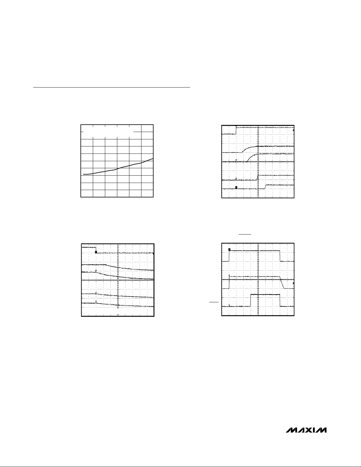
Typical Operating Characteristics (continued)
(Circuit of Figure 3, V
IN1
= V
IN2
= V
IN3
= 3.6V, PWRON = IN, V
BUCK1
= 1.375V, V
BUCK2
= 1.8V, V
OUT1
= 2.6V, V
OUT2
= 2.6V, V
OUT3
= 1.8V, V
OUT4
= 3.0V, SEL1 = SEL2 = open, LX1 = LX2 = Murata LQH32CN2R2M53, TA= +25°C, unless otherwise noted.)
OUT1 OUPUT VOLTAGE
vs. INPUT VOLTAGE
MAX8621 toc05
INPUT VOLTAGE (V)
OUTPUT VOLTAGE (V)
5.04.54.03.53.0
2.525
2.550
2.575
2.600
2.625
2.650
2.500
2.5 5.5
LOAD = 0
LOAD = 300mA
FALLING
RISING
OUT2 OUTPUT VOLTAGE ACCURACY
vs. LOAD CURRENT
MAX8621 toc06
LOAD CURRENT (mA)
OUTPUT VOLTAGE ACCURACY (%)
25020050 100 150
-1.5
-1.0
-0.5
0
0.5
1.0
1.5
2.0
-2.0
0 300
OUT4 DROPOUT VOLTAGE
vs. LOAD CURRENT
MAX8621 toc07
LOAD CURRENT (mA)
DROPOUT VOLTAGE (mV)
10050
20
40
60
80
100
120
140
160
0
0 150
OUT1 POWER-SUPPLY
RIPPLE REJECTION vs. FREQUENCY
MAX8621 toc08
FREQUENCY (kHz)
POWER-SUPPLY RIPPLE REJECTION (dB)
100101
10
20
30
40
50
60
70
80
0
0.1 1000
EFFICICENCY vs. LOAD CURRENT
(V
BUCK2
= 1.8V)
MAX8621 toc09
LOAD CURRENT (mA)
EFFICIENCY (%)
100101
50
60
70
80
90
100
40
0.1 1000
2.2µH
4.7µH
1µH
BUCK1, OUT1, OUT2:
ON WITH NO LOAD
EFFICICENCY vs. LOAD CURRENT
(V
BUCK1
= 1.375V)
MAX8621 toc10
LOAD CURRENT (mA)
EFFICIENCY (%)
100101
50
60
70
80
90
100
40
0.1 1000
2.2µH
4.7µH
1µH
BUCK2, OUT1, OUT2:
ON WITH NO LOAD
Page 8
MAX8621Y/MAX8621Z
Dual Step-Down DC-DC Power-Management ICs
for Portable Devices
8 _______________________________________________________________________________________
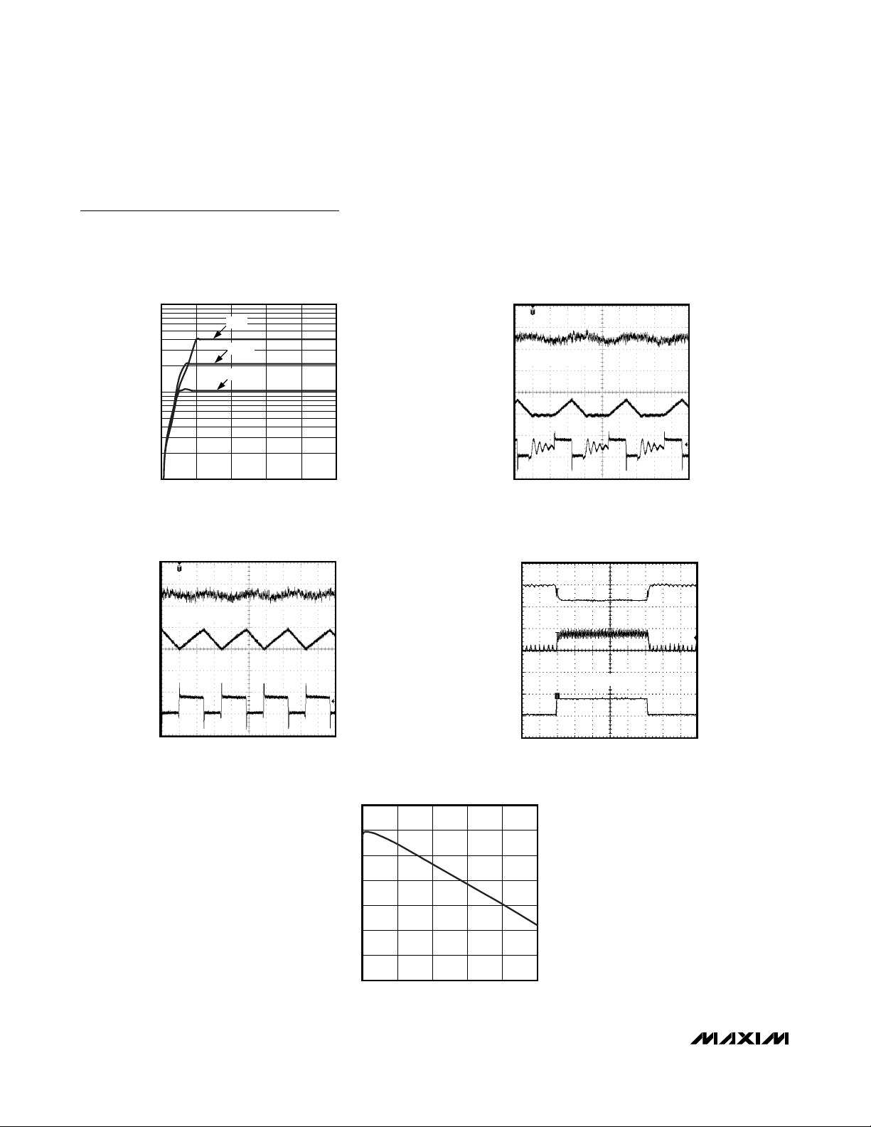
Typical Operating Characteristics (continued)
(Circuit of Figure 3, V
IN1
= V
IN2
= V
IN3
= 3.6V, PWRON = IN, V
BUCK1
= 1.375V, V
BUCK2
= 1.8V, V
OUT1
= 2.6V, V
OUT2
= 2.6V, V
OUT3
= 1.8V, V
OUT4
= 3.0V, SEL1 = SEL2 = open, LX1 = LX2 = Murata LQH32CN2R2M53, TA= +25°C, unless otherwise noted.)
SWITCHING FREQUENCY
vs. LOAD CURRENT
10
1µH
2.2µH
4.7µH
1
FREQUENCY (MHz)
0.1
100 200 300 400
0 500
LOAD CURRENT (mA)
MAX8621 toc11
V
BUCK1 HEAVY-LOAD WAVEFORMS
BUCK1
LOAD = 300mA
I
LX1
V
LX1
MAX8621 toc13
10mV/div
AC-COUPLED
200mA/div
0
5V/div
0
V
BUCK1 LIGHT-LOAD WAVEFORMS
BUCK1
LOAD = 50mA
I
LX1
V
LX1
200ns/div
BUCK1 LOAD-TRANSIENT RESPONSE
V
BUCK1
I
LX1
400mA LOAD
I
BUCK1
MAX8621 toc12
MAX8621 toc14
10mV/div
AC-COUPLED
200mA/div
0
5V/div
0
50mV/div
AC-COUPLED
500mA/div
0
500mA/div
0
200ns/div
5µs/div
BUCK1 OUTPUT VOLTAGE
vs. LOAD CURRENT (VOLTAGE POSITIONING)
1.44
1.42
1.40
1.38
1.36
OUTPUT VOLTAGE (V)
1.34
1.32
1.30
0 500
LOAD CURRENT (mA)
400300200100
MAX8621 toc15
Page 9

MAX8621Y/MAX8621Z
Dual Step-Down DC-DC Power-Management ICs
for Portable Devices
_______________________________________________________________________________________ 9
Pin Description
PIN NAME FUNCTION
1 FB1 Voltage Feedback for Step-Down Converter 1. FB1 regulates to 0.6V nominal.
2 FB2 Voltage Feedback for Step-Down Converter 2. FB2 regulates to 0.6V nominal.
3 GND Ground. Ground for all LDOs and the control section.
4 REFBP
5 EN4 Enable Input for OUT4. Drive EN4 high to turn on OUT4.
6 OUT4
7 EN3 Enable Input for OUT3. Drive EN3 high to turn on OUT3.
8 EN2
9 OUT2
10 IN2
11 RESET
12 OUT1 300m A LD O1 O utp ut. Byp ass w i th a 4.7µF cer am i c cap aci tor to G N D . OU T1 i s hi g h i m p ed ance w hen d i sab l ed .
13 OUT3
14 PWRON
15 ENDR
16 IN3
17 SEL2
18 SEL1
19 DR
20 PGND2 Power Ground for BUCK2 and DR Switch
21 LX2
22 IN1
23 LX1
24 PGND1 Power Ground for BUCK1
— EP Exposed Paddle. Connect the exposed paddle to GND, PGND1, and PGND2.
Reference Noise Bypass. Connect a 0.01µF ceramic capacitor from REFBP to GND. Not intended to drive resistive
load. REFBP is high impedance in shutdown.
150mA LDO4 output. Bypass OUT4 to GND with a 2.2µF ceramic capacitor. OUT4 is high impedance when
disabled. OUT4 can only be activated if OUT1 is within 87% of regulation.
Enable Input for OUT2. Drive EN2 high to disable OUT2. Drive EN2 low or leave open to enable OUT2. EN2 is
internally pulled to GND by an 800kΩ (typ) pulldown resistor. If the MAX8621Y/MAX8621Z are placed into shutdown
using PWRON (PWRON = low), OUT2 does not power regardless of the status of EN2.
300mA LDO2 Output. Bypass with a 4.7µF ceramic capacitor to GND. OUT2 is high impedance when disabled.
OUT2 can only be activated if OUT1 is within 87% of regulation.
Supply Voltage to the Output MOSFET of All 4 LDOs. IN2 must be shorted to IN1 and IN3. Connect a 4.7µF ceramic
capacitor from IN2 to GND.
Open-Drain, Active-Low Reset Output. RESET asserts low when V
deasserts 60ms after V
150mA LDO3 Output. Bypass OUT3 to GND with a 2.2µF ceramic capacitor. OUT3 is high impedance when
disabled. OUT3 can only be activated if OUT1 is within 87% of regulation.
Power Enable Input. Drive PWRON high to enable the MAX8621Y/MAX8621Z. Drive PWRON low to enter shutdown
mode. PWRON has an internal 800kΩ (typ) pulldown resistor.
Enable Input for DR. Drive ENDR low for DR to go into high impedance. Drive ENDR high to activate DR, pulling
DR low.
Supply Voltage to the Control Section. IN3 must be shorted to IN1 and IN2. Connect a 4.7µF ceramic capacitor from
IN3 to GND.
LDO Output-Voltage Select Input 2. SEL1 and SEL2 set the OUT1, OUT2, OUT3, and OUT4 voltages to one of nine
combinations (Table 1).
LDO Output-Voltage Select Input 1. SEL1 and SEL2 set the OUT1, OUT2, OUT3, and OUT4 voltages to one of nine
combinations (Table 1).
200mA Driver Output. Connects to the open drain of an internal n-channel MOSFET whose gate is controlled by
ENDR.
Inductor Connection for BUCK2. LX2 is internally connected to the drain of the internal p-channel MOSFET and the
drain of the internal n-channel synchronous rectifier for BUCK2. LX2 is high impedance when BUCK2 is disabled.
Supply Voltage to the Output Stage of BUCK1 and BUCK2. IN1 must be shorted to IN2 and IN3. Connect a 10µF
ceramic capacitor from IN1 to GND.
Inductor Connection for BUCK1. LX1 is internally connected to the drain of the internal p-channel MOSFET and the
drain of the internal n-channel synchronous rectifier for BUCK1. LX1 is high impedance when BUCK1 is disabled.
rises above 87% (typ) of regulation (Figure 2).
OUT1
drops below 87% (typ) of regulation. RESET
OUT1
Page 10

MAX8621Y/MAX8621Z
Dual Step-Down DC-DC Power-Management ICs
for Portable Devices
10 ______________________________________________________________________________________
Detailed Description
The MAX8621Y/MAX8621Z power-management ICs are
designed specifically to power a variety of portable
devices including cellular handsets. Each device contains two 4MHz high-efficient step-down converters, four
low-dropout linear regulators (LDOs), a 60ms (typ) reset
timer, a 200mA open-drain output driver, and poweron/off control logic (Figure 3).
Step Down DC-DC Control Scheme
The MAX8621Y/MAX8621Z step-down converters are
optimized for high-efficiency voltage conversion over a
wide load range, while maintaining excellent transient
response, minimizing external component size, and
minimizing output voltage ripple. The DC-DC converters (BUCK1 and BUCK2) also feature an optimized onresistance internal MOSFET switch and synchronous
rectifier to maximize efficiency. The MAX8621Y/
MAX8621Z utilize a proprietary hysteretic-PWM control
scheme that switches with nearly fixed frequency up to
4MHz, allowing for ultra-small external components.
The step-down converter output current is guaranteed
up to 500mA, while consuming 40µA (typ).
When the step-down converter output voltage falls below
the regulation threshold, the error comparator begins a
switching cycle by turning the high-side p-channel
MOSFET switch on. This switch remains on until the minimum on-time (tON) expires and the output voltage is in
regulation or the current-limit threshold (I
LIMP
) is exceeded. Once off, the high-side switch remains off until the
minimum off-time (t
OFF
) expires and the output voltage
again falls below the regulation threshold. During this off
period, the low-side synchronous rectifier turns on and
remains on until either the high-side switch turns on or
the inductor current reduces to the rectifier-off current
threshold (I
LXOFF
= 45mA (typ)). The internal synchronous rectifier eliminates the need for an external
Schottky diode.
Voltage-Positioning Load Regulation
The MAX8621Y/MAX8621Z use a unique step-down
converter feedback network. By taking feedback from
the LX node through R1, the usual phase lag due to the
output capacitor is removed, making the loop exceedingly stable and allowing the use of a very small ceramic
output capacitor. This configuration causes the output
voltage to shift by the inductor series resistance multiplied by the load current. This output voltage shift is
known as voltage-positioning load regulation. Voltagepositioning load regulation greatly reduces overshoot
during load transients, which effectively halves the
peak-to-peak output-voltage excursions compared to
traditional step-down converters. See the Buck1 Load-
Transient Response graph in the Typical Operating
Characteristics.
Low-Dropout Linear Regulators
Each MAX8621Y/MAX8621Z contains four low-dropout,
low-quiescent-current, high-accuracy linear regulators
(LDOs). OUT1 and OUT2 supply loads up to 300mA,
while OUT3 and OUT4 supply loads up to 150mA. The
LDO output voltages are set using SEL1 and SEL2 (see
Table 1). The LDOs include an internal reference, error
amplifier, p-channel pass transistor, internal programmable voltage-divider, and an OUT1 power-good comparator. Each error amplifier compares the reference
voltage to a feedback voltage and amplifies the difference. If the feedback voltage is lower than the reference voltage, the pass-transistor gate is pulled lower,
allowing more current to pass to the outputs and
increasing the output voltage. If the feedback voltage is
too high, the pass-transistor gate is pulled up, allowing
less current to pass to the output.
DR Driver
Each MAX8621Y/MAX8621Z includes a 1.3Ω n-channel
MOSFET open-drain output that is controlled by ENDR.
This output can be used to drive LEDs (see the Typical
Operating Circuit) and allow adjustable output voltages
(see Figure 1).
Programming LDO Output Voltages
(SEL1, SEL2)
As shown in Table 1, the LDO output voltages, OUT1,
OUT2, OUT3, and OUT4 are pin-programmable by the
logic states of SEL1 and SEL2. SEL1 and SEL2 are
trilevel inputs: IN, open, and GND. The input voltage,
VIN, must be greater than the selected OUT1, OUT2,
OUT3, and OUT4 voltages. The logic states of SEL1
and SEL2 can be programmed only during power-up.
Once the OUT_ voltages are programmed, their values
do not change by changing SEL_ unless the
MAX8621Y/MAX8621Z power is cycled.
Figure 1. Adjusting BUCK1 Output Voltage Using DR
L1
2.2µH
LX1
R1
FB1
150kΩ
R5
215kΩ
DR
MAX8621Y
MAX8621Z
1.38/1.8
ENDR
C6
150pF
R2
115kΩ
BUCK1
1.38V OR 1.8V
Page 11

Power-Supply Sequence
BUCK1 is always first on and last off in the MAX8621Y/
MAX8621Zs’ power sequence. BUCK1 turns on approximately 40µs after PWRON is enabled. BUCK2 turns on
approximately 40µs after BUCK1, and OUT1 turns on
65µs after BUCK2. These delays have been added to
sequence the turn-on of the step-down converters and
LDOs so that the initial current surges are distributed
over time. For the same reason, OUT2, OUT3, and OUT4
can be turned on by EN2, EN3, and EN4 signals, but
only after OUT1 has reached 87% of its final value. Note
that OUT2 typically requires a longer time to enable than
OUT3 and OUT4 (45µs versus 15µs). All regulators can
be turned off at the same time when PWRON is low, but
BUCK1 remains on for approximately another 120µs
after PWRON goes low.
MAX8621Y/MAX8621Z
Dual Step-Down DC-DC Power-Management ICs
for Portable Devices
______________________________________________________________________________________ 11
Table 1. SEL1 and SEL2, MAX8621Y/MAX8621Z Output Voltage Selection
Figure 2. Power-On/Off Sequence Diagram
SEL1 SEL2
IN IN 3.3 3.3 2.85 2.85 2.8 2.6 3.0 3.0
IN OPEN 3.0 3.3 3.3 2.85 2.6 2.6 3.0 3.0
IN GND 2.5 3.3 2.85 3.0 2.6 2.6 2.9 2.9
OPEN IN 2.85 3.3 3.0 2.5 2.6 2.6 3.0 3.3
OPEN OPEN 3.3 3.3 2.8 3.0 2.6 2.6 1.8 3.0
OPEN GND 3.3 3.3 3.0 3.0 2.6 2.6 2.8 3.0
GND IN 3.3 2.85 3.3 2.85 2.9 3.1 1.8 1.5
GND OPEN 2.85 2.85 3.3 3.3 3.0 2.9 2.9 2.9
GND GND 3.3 2.85 3.0 3.0 3.0 2.5 2.9 2.9
OUT1 (V) OUT2 (V) OUT3 (V) OUT4 (V) OUT1 (V) OUT2 (V) OUT3 (V) OUT4 (V)
MAX8621Y MAX8621Z
PWRON
REF
BUCK1
BUCK2
OUT1
RESET
OUT2
EN3
(EN4)
OUT3
(OUT4)
EN2
40µs
40µs
65µs
15µs
87% REGULATION
60ms
45µs
120µs
87% REGULATION
Page 12

MAX8621Y/MAX8621Z
PWRON
Drive PWRON low or leave PWRON open to place the
MAX8621Y/MAX8621Z in power-down mode and
reduce supply current to 5µA (typ). In power-down, the
control circuitry, internal-switching p-channel MOSFET,
and the internal synchronous rectifier (n-channel
MOSFET) turn off (BUCK1 and BUCK2), and LX_
becomes high impedance. In addition, all four LDOs
are disabled. Connect PWRON to IN or logic-high to
enable the MAX8621Y/MAX8621Z. EN2 enables and
disables OUT2 when PWRON is high.
OUT2 Enable (
EN2
)
Drive EN2 high to disable OUT2. Drive EN2 low or
leave open to enable OUT2. EN2 is internally pulled to
GND by an 800kΩ (typ) pulldown resistor. If the
MAX8621Y/MAX8621Z are powered down using
PWRON (PWRON = low), OUT2 does not power
regardless of the status of EN2.
Reset Output (
RESET
)
The reset circuit is active both at power-up and powerdown. RESET asserts low when V
OUT1
drops below
87% (typ) of regulation. RESET deasserts 60ms after
V
OUT1
rises above 87% (typ) of regulation. RESET is
pulled up through an internal 14kΩ resistor to OUT1.
Undervoltage Lockout
Initial power-up of the MAX8621Y/MAX8621Z occurs
when VINis greater than 2.85V (typ) and PWRON
asserts. Once VINexceeds 2.85V (typ), the undervoltage lockout has 0.5V of hysteresis, allowing the V
IN
operating range to drop down to 2.35V (typ) without
shutting down.
Current Limiting
The MAX8621Y/MAX8621Z OUT1 and OUT2 LDOs limit
their output current to 550mA (typ). OUT3 and OUT4
LDOs limit their output current to 360mA (typ). If the LDO
output current exceeds the current limit, the corresponding LDO output voltage drops. The step-down converters
(BUCK1 and BUCK2) limit the p-channel MOSFET to
670mA (min) and the n-channel MOSFET to 750mA (min).
Reference Bypass Capacitor
Node (REFBP)
An external 0.01µF bypass capacitor and an internal
100kΩ (typ) resistor at REFBP create a lowpass filter for
LDO noise reduction. OUT1, OUT2, OUT3, and OUT4
exhibit 45µV
RMS
of output voltage noise with C
REFBP
=
0.01µF, C
OUT1
= C
OUT2
= 4.7µF, and C
OUT3
= C
OUT4
= 2.2µF.
Thermal-Overload Protection
Thermal-overload protection limits total power dissipation in the MAX8621Y/MAX8621Z. Independent thermalprotection circuits monitor the step-down converters
and the linear-regulator circuits. When the junction temperature exceeds TJ= +160°C, the thermal-overload
protection circuit disables the corresponding circuitry,
allowing the IC to cool. The LDO thermal-overload protection circuit enables the LDOs after the LDO junction
temperature cools down, resulting in pulsed LDO outputs during continuous thermal-overload conditions. The
step-down converter’s thermal-overload protection
circuitry enables the step-down converter after the
junction temperature cools down. Thermal-overload
protection safeguards the MAX8621Y/MAX8621Z in the
event of fault conditions. For continuous operation, do
not exceed the absolute maximum junction-temperature
rating of T
J
= +150°C.
Applications Information
Step-Down DC-DC Converter
Setting the Step-Down Output Voltage
Select an output voltage for BUCK1 between 0.6V and
3.3V by connecting FB1 to a resistive voltage-divider
between LX1 and GND. Choose R2 (Figure 3) for a rea-
sonable bias current in the resistive divider. A wide range
of resistor values is acceptable, but a good starting point
is to choose R2 as 100kΩ. Then, R1 (Figure 3) is given by:
where VFB= 0.6V. For BUCK2, R3 and R4 are calculated
using the same methods.
Input Capacitor
The input capacitor, C
IN1
, reduces the current peaks
drawn from the battery or input power source and
reduces switching noise in the IC. The impedance of
C
IN1
at the switching frequency should be kept very
low. Ceramic capacitors with X5R or X7R dielectrics are
highly recommended due to their small size, low ESR,
and small temperature coefficients. Due to the
MAX8621Y/MAX8621Z step-down converter’s fast softstart, the input capacitance can be very low. Use a
10µF ceramic capacitor or an equivalent amount of
multiple capacitors in parallel between IN1 and ground.
Connect C
IN1
as close to the IC as possible to minimize
the impact of PC board trace inductance. Use a 4.7µF
ceramic capacitor from IN2 to ground and a second
4.7µF ceramic capacitor from IN3 to ground.
Dual Step-Down DC-DC Power-Management ICs
for Portable Devices
12 ______________________________________________________________________________________
⎛
RR
12 1=
V
⎜
V
⎝
OUT
FB
⎞
−
⎟
⎠
Page 13

Inductor Selection
The MAX8621Y/MAX8621Z step-down converters operate with inductors between 1µH and 4.7µH. Low-inductance values are physically smaller but require faster
switching, resulting in some efficiency loss. See the
Typical Operating Characteristics for efficiency and
switching frequency vs. inductor value plots. The
inductor’s DC current rating needs to be only 100mA
greater than the application’s maximum load current
because the step-down converter features zero-current
overshoot during startup and load transients.
For output voltages above 2.0V, when light-load efficiency is important, the minimum recommended inductor is 2.2µH. For optimum voltage-positioning load
transients, choose an inductor with DC series resistance in the 50mΩ to 150mΩ range. For higher efficiency at heavy loads (above 200mA) or minimal load
regulation (but some transient overshoot), the resistance should be kept below 100mΩ. For light-load
applications up to 200mA, much higher resistance is
acceptable with very little impact on performance. See
Table 2 for some suggested inductors.
MAX8621Y/MAX8621Z
Dual Step-Down DC-DC Power-Management ICs
for Portable Devices
______________________________________________________________________________________ 13
Table 2. Suggested Inductors
MANUFACTURER SERIES
CB2012
LB2012
LB2016
Taiyo Yuden
LB2518
LBC2518
LQH32C_53
Murata
LQM43FN
D310F
TOKO
D312C
Sumida CDRH2D11
INDUCTANCE
(µH)
2.2
4.7
1.0
2.2
1.0
1.5
2.2
3.3
1.0
1.5
2.2
3.3
1.0
1.5
2.2
3.3
4.7
1.0
2.2
4.7
2.2
4.7
1.5
2.2
3.3
1.5
2.2
2.7
3.3
1.5
2.2
3.3
4.7
ESR
(Ω)
0.23
0.40
0.15
0.23
0.09
0.11
0.13
0.20
0.06
0.07
0.09
0.11
0.08
0.11
0.13
0.16
0.20
0.06
0.10
0.15
0.10
0.17
0.13
0.17
0.19
0.10
0.12
0.15
0.17
0.05
0.08
0.10
0.14
CURRENT RATING
(mA)
410
300
300
240
455
350
315
280
500
400
340
270
775
660
600
500
430
1000
790
650
400
300
1230
1080
1010
1290
1140
980
900
900
780
600
500
DIMENSIONS
2.0 x 1.25 x 1.25
= 3.1mm
2.0 x 1.25 x 1.25
= 3.1mm
2.0 x 1.6 x 1.8
= 5.8mm
2.5 x 1.8 x 2.0
2.5 x 1.8 x 2.0
3.2 x 2.5 x 1.7
= 14mm
4.5 x 3.2 x 0.9
= 13mm
3.6 x 3.6 x 1.0
= 13mm
3.6 x 3.6 x 1.2
= 16mm
3.2 x 3.2 x 1.2
= 12mm
= 9mm
= 9mm
3
3
3
3
3
3
3
3
3
3
Page 14

MAX8621Y/MAX8621Z
Output Capacitor
The output capacitors, C7 and C9 in Figure 3, are
required to keep the output voltage ripple small and to
ensure regulation loop stability. C7 and C9 must have
low impedance at the switching frequency. Ceramic
capacitors with X5R or X7R dielectric are highly recommended due to their small size, low ESR, and small
temperature coefficients. Due to the unique feedback
network, the output capacitance can be very low. For
most applications, a 2.2µF capacitor is sufficient. For
optimum load-transient performance and very low output ripple, the output capacitor value in µF should be
equal or larger than the inductor value in µH.
Feed-Forward Capacitor
The feed-forward capacitors, CFF(C6 and C8 in Figure
3), set the feedback loop response, control the switching frequency, and are critical in obtaining the best efficiency possible. Choose a small ceramic X7R
capacitor with value given by:
Select the closest standard value to C
FF
as possible.
For BUCK2, C8, R3, and L1 are calculated using the
same methods.
LDO Output Capacitor and
Regulator Stability
Connect a 4.7µF ceramic capacitor between OUT1 and
ground, and a second 4.7µF ceramic capacitor
between OUT2 and ground for 300mA applications. For
150mA applications, 2.2µF ceramic capacitors can be
used for OUT1 and OUT2. Connect a 2.2µF ceramic
capacitor between OUT3 and ground, and a second
2.2µF ceramic capacitor between OUT4 and ground.
The LDO output capacitor’s (C
OUT
) equivalent series
resistance (ESR) affects stability and output noise. Use
output capacitors with an ESR of 0.1Ω or less to ensure
stability and optimum transient response. Surfacemount ceramic capacitors have very low ESR and are
commonly available in values up to 10µF. Connect
C
OUT_
as close to the IC as possible to minimize the
impact of PC board trace inductance.
Thermal Considerations
The MAX8621Y/MAX8621Z total power dissipation, PD,
is estimated using the following equations:
where P
IN(BUCK1)
is the input power for BUCK1, η is the
step-down converter efficiency, and R
DC(INDUCTOR)
is
the inductor’s DC resistance.
For example, operating with V
IN
= 3.7V, V
BUCK1
= 1.376V,
V
BUCK2
= 1.8V, V
OUT1
= V
OUT2
= 2.6V, V
OUT3
= 1.8V,
V
OUT4
= 3V, I
BUCK1
= I
BUCK2
= 300mA, I
OUT1
= I
OUT2
=
330mA, I
OUT3
= I
OUT4
= 100mA, P
IN(BUCK1)
= 516mW
and η = 80%, P
IN(BUCK2)
= 651mW and η = 83%:
Dual Step-Down DC-DC Power-Management ICs
for Portable Devices
14 ______________________________________________________________________________________
L
1
C
Siemens6
10=×
R
1
PP P P
=+ +
D LOSS BUCK LOSS BUCK LOSS OUT
PP
LOSS BUCK IN BUCK
PP
LOSS BUCK IN BUCK
PIVV
LOSS OUT OUT IN OUT
PIVV
LOSS OUT OUT IN OUT
PIVV
LOSS OUT OUT IN OUT
PIVV
LOSS OUT OUT IN OUT
() ( ) ()
121
PPP
+++
LOSS OUT LOSS OUT LOSS OUT
() () ()
234
()()
()()
()
()
()
()
=×
11
2
−
IR
BUCK DC INDUCTOR
=×
22
−
IR
BUCK DC
=×
11 1
=×
22 2
=×
33 3
=×
44 4
×
1
2
2
−
()
()
()
()
/
−
1 100
η
()
()
/
1 100
η
−
()
×
(
INDUCTORINDUCTOR
−
−
−
)
PP mW
LOSS OUT LOSS OUT
PmW
LOSS OUT
PmW
LOSS OUT
PmW
LOSS BUCK
PmW
LOSS BUCK
PmWmWmWmW
363 363 190 70
=+++
D
++ =
==
() ( )
12
()
()
()
()
=
3
=
4
=
1
2
mW mW mW
94 102 1182
190
70
94
102
=
363
Page 15

MAX8621Y/MAX8621Z
Dual Step-Down DC-DC Power-Management ICs
for Portable Devices
______________________________________________________________________________________ 15
Figure 3. Functional Diagram and Typical Application Schematic
0.01µF
2.2µF
2.2µF
C4
C11
C12
INPUT
2.6V TO 5.5V
REFBP
GND
DR
ENDR
OUT3
EN3
OUT4
PGND2
OUT
OUT
N
LDO3
GND
LDO4
UVLO
REF
1.3Ω, 200mA
INP
REF
EN
9-BIT SEL
INP
REF
IN
IN
4.7µF
C3
IN3
C2
4.7µF
IN2
IN
REF
EN
IN
REF
EN
INP
IN
REF
LDO1
EN
9-BIT SEL
GND
STEP-DOWN
DC-DC (1, BUCK1)
STEP-DOWN
DC-DC (2, BUCK2)
INP
IN
REF
LDO2
EN
9-BIT SEL
GND
RESET
OUT
INP
PGND
INP
PGND
OUT
LX
FB
IN1
LX
FB
14kΩ
OUT1
RESET
IN1
P
LX1
N
150k
PGND1
FB1
P
LX2
N
150kΩ
PGND2
FB2
OUT2
C5
4.7µF
INPUT
2.6V TO 5.5V
C1
L1
2.2µH
R1
Ω
R3
R2
115kΩ
2.2µH
R4
75kΩ
C10
4.7µF
L2
C6
150pF
C8
150pF
10µF
BUCK1
C7
2.2µF
BUCK2
C9
2.2µF
EN
9-BIT SEL
GND
EN4
PWRON
800kΩ
ON/OFF CONTROL
VOLTAGE
SELECTOR
THERMAL
SHUTDOWN
800kΩ
MAX8621Y
MAX8621Z
EN2
SEL1
SEL2
Page 16

The die junction temperature can be calculated as follows:
When operating at an ambient temp of +70°C under the
above conditions:
TJshould not exceed +150°C in normal operating conditions.
Printed Circuit Board Layout and Routing
High switching frequencies and relatively large peak
currents make the PC board layout a very important
aspect of design. Good design minimizes excessive
EMI on the feedback paths and voltage gradients in the
ground plane, both of which can result in instability or
regulation errors. Connect C
IN_
close to IN_ and GND.
Connect the inductor and output capacitors (C
OUT_
) as
close to the IC as possible and keep the traces short,
direct, and wide.
The traces between C
OUT_
, C
FF_
, and FB_ are sensitive
to inductor magnetic field interference. Route these
traces between ground planes or keep the traces away
from the inductors.
Connect GND and PGND_ to the ground plane. The
external feedback network should be very close to the
FB pin, within 0.2in (5mm). Keep noisy traces, such as
the LX node, as short as possible. Connect GND to the
exposed paddle directly under the IC. Refer to the
MAX8621Y/MAX8621Z evaluation kit for an example PC
board layout and routing.
MAX8621Y/MAX8621Z
Dual Step-Down DC-DC Power-Management ICs
for Portable Devices
16 ______________________________________________________________________________________
Pin Configuration
Chip Information
TRANSISTOR COUNT: 5850
PROCESS: BiCMOS
TTP
=+×θ
JADJA
C
°
⎛
⎞
TC W
=°+
J
⎜
⎝
=°70 1 182 36 112 6..
⎟
⎠
W
C
TOP VIEW
DR
PGND2
LX2
IN1
LX1
PGND1
19
20
21
22
23
24
SEL1
SEL2
IN3
MAX8621Y
MAX8621Z
ENDR
PWRON
131415161718
OUT3
OUT1
12
RESET
11
IN2
10
OUT2
9
EN2
8
EN3
7
543
REFBP
6
EN4
1
2
FB2
FB1
GND
OUT4
Page 17

MAX8621Y/MAX8621Z
Dual Step-Down DC-DC Power-Management ICs
for Portable Devices
______________________________________________________________________________________ 17
Package Information
(The package drawing(s) in this data sheet may not reflect the most current specifications. For the latest package outline information
go to www.maxim-ic.com/packages
.)
24L QFN THIN.EPS
PACKAGE OUTLINE
12, 16, 20, 24L THIN QFN, 4x4x0.8mm
21-0139
1
C
2
Page 18

MAX8621Y/MAX8621Z
Dual Step-Down DC-DC Power-Management ICs
for Portable Devices
Maxim cannot assume responsibility for use of any circuitry other than circuitry entirely embodied in a Maxim product. No circuit patent licenses are
implied. Maxim reserves the right to change the circuitry and specifications without notice at any time.
18 ____________________Maxim Integrated Products, 120 San Gabriel Drive, Sunnyvale, CA 94086 408-737-7600
© 2005 Maxim Integrated Products Printed USA is a registered trademark of Maxim Integrated Products, Inc.
Package Information (continued)
(The package drawing(s) in this data sheet may not reflect the most current specifications. For the latest package outline information
go to www.maxim-ic.com/packages
.)
PACKAGE OUTLINE
12, 16, 20, 24L THIN QFN, 4x4x0.8mm
21-0139
2
C
2
 Loading...