

Page 1

General Description
The MAX8620Y micro-power-management integrated
circuit (µPMIC) powers low-voltage microprocessors or
DSPs in portable devices. The µPMIC includes a highefficiency step-down DC-DC converter, two lowdropout linear regulators (LDOs), a microprocessor
reset output, and power-on/off control logic. This device
maintains high efficiency at light loads with a low 115µA
supply current, and its miniature TDFN package makes
it ideal for portable devices.
The MAX8620Y’s step-down DC-DC converter utilizes a
proprietary 4MHz hysteretic-PWM control scheme that
allows for ultra-small external components. Internal synchronous rectification improves efficiency and eliminates the external Schottky diode that is required in
conventional step-down converters. The output voltage
is adjustable from 0.6V to 3.3V, with guaranteed output
current up to 500mA.
The MAX8620Y’s two LDOs offer low 45µV
RMS
output
noise and a low dropout of only 200mV at 200mA. Each
LDO delivers at least 300mA of continuous output current. The output voltages are pin selectable from 1.8V
to 3.3V for flexibility.
A microprocessor reset output (RESET) monitors OUT1
and warns the system of impending power loss allowing safe shutdown. RESET asserts during power-up,
power-down, shutdown, and fault conditions where
V
OUT1
is below its regulation voltage.
Applications
Cellular Handsets
Smart Phones/PDA Phones
PDAs
Wireless LAN
Microprocessor and DSP Solutions including
MSM™, XScale™, ARM™, and OMAP™
Features
♦ Three Regulators and a Reset in One Package
♦ High-Efficiency Step-Down Converter
Up to 4MHz Fixed Switching Frequency
500mA Guaranteed Output Current
0.6V to 3.3V Adjustable Output Voltage
±2% Initial Accuracy
Fast Voltage-Positioning Transient Response
Internal Synchronous Rectifier
♦ Two 300mA LDO Regulators
200mV Dropout at 200mA Load
Low 45µV
RMS
Output Noise
3% Accuracy over Line, Load, and Temperature
Overcurrent Protection
Nine Pin-Selectable Output-Voltage Settings
♦ 30ms (min) RESET Output Flag
♦ 2.7V to 5.5V Input
♦ 115µA (typ) Supply Current at No Load
♦ Thermal-Overload Protection
♦ Tiny 3mm x 3mm x 0.8mm TDFN Package
MAX8620Y
µPMIC for Microprocessors or DSPs
in Portable Equipment
________________________________________________________________ Maxim Integrated Products 1
Ordering Information
Typical Operating Circuit
19-3564; Rev 0; 1/05
For pricing, delivery, and ordering information, please contact Maxim/Dallas Direct! at
1-888-629-4642, or visit Maxim’s website at www.maxim-ic.com.
MSM is a trademark of QUALCOMM, Inc.
XScale is a trademark of Intel Corp.
ARM is a trademark of ARM Limited.
OMAP is a trademark of Texas Instruments, Inc.
EVALUATION KIT
AVAILABLE
Pin Configuration appears at end of data sheet.
PART TEMP RANGE
MAX8620YETD -40°C to +85°C
PINPACKAGE
14 TDFN-EP
(T1433-2)
TOP
MARK
AAB
V
OUT1
V
LOGIC
AND V
100kΩ
1.80V, 2.60V, 2.80V, 2.85V,
3.00V, OR 3.30V*
300mA
1.80V, 2.50V, 2.60V,
2.85V, OR 3.00V*
300mA
RESET
OUT2
IN
IN2
IN1
MAX8620Y
BP
EN2
HF_PWR
PWR_ON
SEL1
SEL2
GND
*USE SEL1 AND SEL2 TO SET V
OUT1
OUT2
RESET
LX
FB
OUT3
0.6V TO 3.3V
500mA
Page 2

MAX8620Y
µPMIC for Microprocessors or DSPs
in Portable Equipment
2 _______________________________________________________________________________________
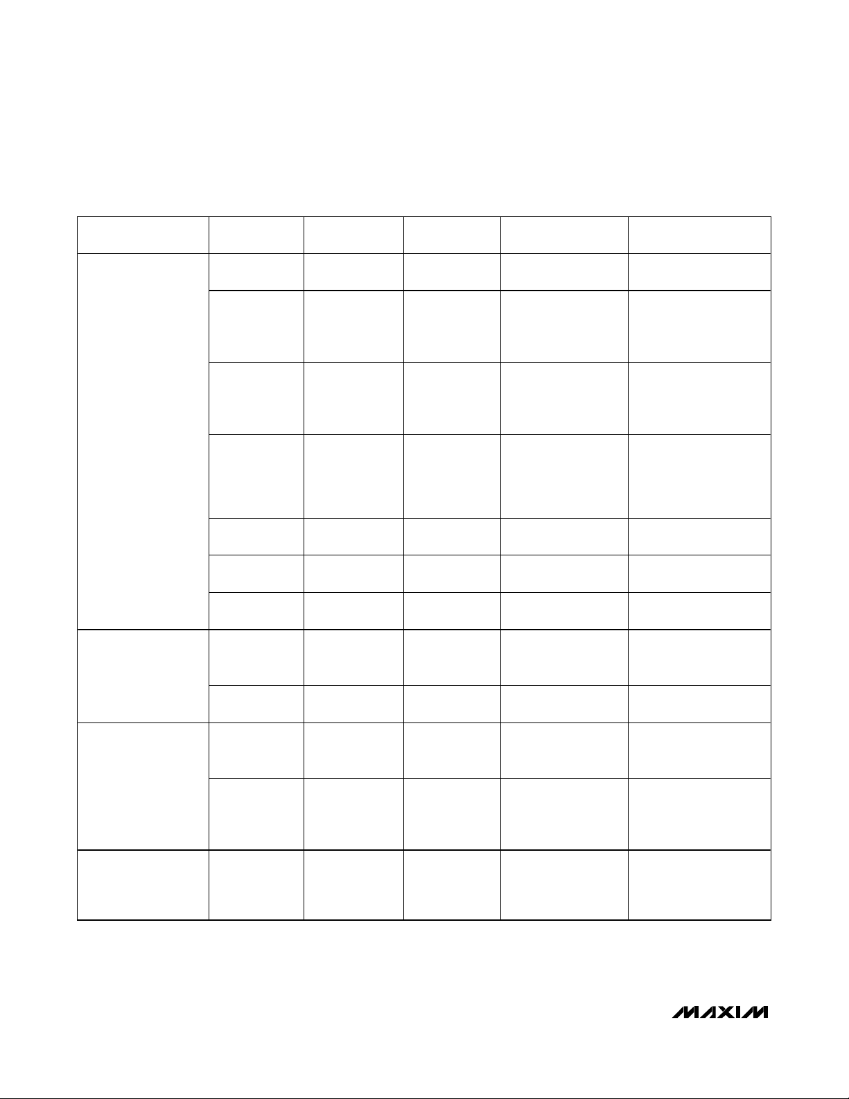
ABSOLUTE MAXIMUM RATINGS
ELECTRICAL CHARACTERISTICS
(V
IN1
= V
IN2
= +3.7V, CIN= 10µF, CBP= 0.01µF, TA= -40°C to +85°C, unless otherwise noted. Typical values are at TA= +25°C.)
(Note 1)
Stresses beyond those listed under “Absolute Maximum Ratings” may cause permanent damage to the device. These are stress ratings only, and functional
operation of the device at these or any other conditions beyond those indicated in the operational sections of the specifications is not implied. Exposure to
absolute maximum rating conditions for extended periods may affect device reliability.
IN1, IN2, PWR_ON, RESET, EN2, SEL1, SEL2,
HF_PWR, FB, BP to GND ..................................-0.3V to +6.0V
OUT1, OUT2 to GND .................................-0.3V to (V
IN1
+ 0.3V)
LX Current ......................................................................1.5A
RMS
Continuous Power Dissipation (TA= +70°C)
14-Pin TDFN (derate 18.2mW/°C above +70°C) .......1454mW
Operating Temperature Range ...........................-40°C to +85°C
Junction Temperature......................................................+150°C
Storage Temperature Range .............................-65°C to +150°C
Lead Temperature (soldering, 10s) .................................+300°C
PARAMETER
SYMBOL
CONDITIONS
MIN
TYP
MAX
UNITS
Supply Voltage Range V
IN1
2.7 5.5 V
Shutdown Supply Current I
SHDN
V
IN1
= V
IN2
= 4.2V, PWR_ON = HF_PWR =
GND
5.5 10 µA
All outputs enabled, no load
140
Supply Current
V
OUT1
= V
OUT3
= 1.8V, I
OUT1
= I
OUT3
=
500µA, OUT2 disabled
µA
UNDERVOLTAGE LOCKOUT
V
IN1
= V
IN2
rising
UVLO Threshold V
UVLO
V
IN1
= V
IN2
falling
V
THERMAL PROTECTION
Thermal-Shutdown Threshold Temperature rising
°C
Thermal-Shutdown Hysteresis 15 °C
REFERENCE (BP)
Reference Bypass Output
Voltage
V
BP
0 ≤ IBP ≤ 1µA
V
LOGIC AND CONTROL INPUTS (PWR_ON, HF_PWR, EN2)
PWR_ON, HF_PWR, EN2 Input
Low Voltage
V
IL
V
IN1
= V
IN2
= 2.7V to 4.2V (Note 2) 0.4 V
PWR_ON, HF_PWR, EN2 Input
High Voltage
V
IH
V
IN1
= V
IN2
= 2.7V to 4.2V (Note 2)
V
Input Bias Current I
INB
V
PWR_ON
= V
HF_PWR
= V
EN2
= 0V or 5.5V -1 +1 µA
HF_PWR Timer t
HF
From the rising edge of HF_PWR until the
one-shot timer expires (Figure 4)
s
LINEAR REGULATORS (OUT1, OUT2)
0°C to +85°C
I
LOAD
= 1mA, 3.7V ≤ V
IN
≤ 5.5V
-40°C to +85°C
1mA ≤ I
LOAD
≤ 300mA
OUT1, OUT2 Output-Voltage
Accuracy
V
OUT2
I
LOAD
= 150mA 0
%
OUT1, OUT2 Output Current I
OUT_
mA
OUT1, OUT2 Output Current Limit
I
LIM_
V
OUT_
= 0V
940 mA
OUT1, OUT2 Dropout Voltage V
DO
I
LOAD
= 200mA, TA = +85°C (Note 3)
380 mV
I
+ I
IN1
IN2
,
V
OUT1
115
430
2.70 2.85 3.05
2.35
+160
1.231 1.250 1.269
1.44
1.05 1.31 1.46
-1.3 +1.8
-1.5 +1.8
-1.2
300
310 550
200
Page 3

MAX8620Y
µPMIC for Microprocessors or DSPs
in Portable Equipment
_______________________________________________________________________________________ 3
ELECTRICAL CHARACTERISTICS (continued)
(V
IN1
= V
IN2
= +3.7V, CIN= 10µF, CBP= 0.01µF, TA= -40°C to +85°C, unless otherwise noted. Typical values are at TA= +25°C.)
(Note 1)
Note 1: Specifications are 100% production tested at T
A
= +25°C. Maximum and minimum limits over temperature are guaranteed
by design and characterization.
Note 2: After startup.
Note 3: Guaranteed by design.
Note 4: RESET asserts low when V
OUT1
drops below the specified percent of the OUT1 regulation voltage.
OUT1, OUT2 Power-Supply
Rejection Ratio
Output Noise Voltage
STEP-DOWN CONVERTER (OUT3)
Output Voltage Range V
FB Threshold Voltage V
FB Threshold Line Regulation V
FB Threshold Voltage Accuracy
(Falling) (% of V
FB Threshold Voltage Hysteresis
(% of V
FB Bias Current I
Current Limit
On-Resistance
Rectifier-Off Current Threshold I
Minimum On- and Off-Times
OPEN-DRAIN, ACTIVE-LOW RESET OUTPUT (RESET)
RESET Output-Voltage Low V
RESET Output Leakage Current V
RESET Threshold Voltage V
RESET Timeout Period t
LDO OUTPUT-VOLTAGE SELECT INPUTS (SEL1, SEL2)
SEL_ Input Low Threshold 1V
SEL_ Input High Threshold V
SEL_ Input Bias Current
PARAMETER SYMBOL CONDITIONS MIN TYP MAX UNITS
TH
f = 10Hz to 10kHz, C
= 30mA
I
LOAD_
f = 100Hz to 100kHz, C
= 30mA
I
LOAD_
f = 100Hz to 100kHz, C
= 30mA, CBP open
I
LOAD_
OUT3
VFB falling 0.6 V
TH
= V
IN1
I
)
TH
V
)
HYS
FB
I
LIM3P
I
LIM3N
R
ONP
R
ONN
LXOFF
t
ON
t
OFF
OL
THR
RP
OUT3
OUT3 disabled 10
V
FB
pFET switch 675 950 1200
nFET rectifier 875 1000 1200
pFET switch, I
nFET rectifier, I
I
SINK
RESET
Percent of the OUT1 regulation voltage
(Note 4)
Figure 4 30 60 ms
V
IN1
V
SEL2
= 2.7V to 5.5V (Note 2) 0.08 %/V
IN2
= 0mA
= 0.5V 10
= -200mA 0.65 1.5
LX
= +200mA 0.35 0.8
LX
= 500µA 0.3 V
= 5.5V 100 nA
= V
= 4.2V, V
IN2
= 0V or V
IN1
= 4.7µF,
OUT_
OUT_
OUT_
= 4.7µF,
= 4.7µF,
60 dB
45
100
0.6 3.3 V
TA = +25°C -2 +2
= -40°C to +85°C -3 +3
T
A
2%
30 60 mA
107
95
84 87 90 %
- 0.2V V
IN_
SEL1
= 0V or V
IN1
,
±0.1 µA
µV
RMS
%
µA
mA
Ω
ns
Page 4
MAX8620Y
µPMIC for Microprocessors or DSPs
in Portable Equipment
4 _______________________________________________________________________________________
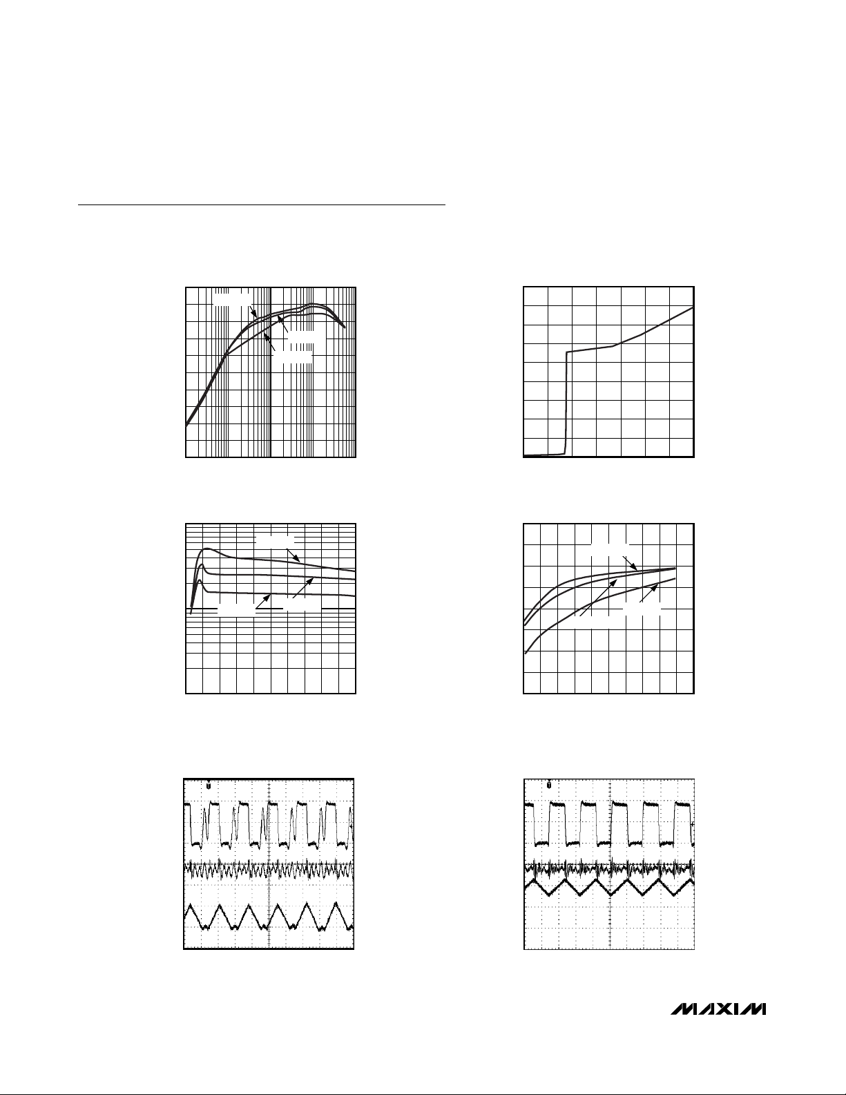
Typical Operating Characteristics
(V
IN1
= V
IN2
= 3.7V, PWR_ON = IN1, L = 2.2µH (LQH31CN2R2M53), CFF= 150pF, V
OUT1
= V
OUT2
= 2.6V, V
OUT3
= 1.867V (R1 =
150kΩ, R2 = 75kΩ), C
IN
= 10µF, C
BP
= 0.01µF, C
OUT1
= C
OUT2
= 4.7µF, C
OUT3
= 2.2µF, RESET pulled up with 100kΩ to OUT1,
T
A
= +25°C, unless otherwise noted.)
EFFICIENCY vs. LOAD CURRENT
MAX8620Y toc01
LOAD CURRENT (mA)
EFFICIENCY (%)
100101
10
20
30
40
50
60
70
80
90
100
0
0.1 1000
L = 4.7µH
L = 2.2µH
L = 1.0µH
INPUT QUIESCENT CURRENT
vs. INPUT VOLTAGE
MAX8620Y toc02
INPUT VOLTAGE (V)
QUIESCENT CURRENT (µA)
5.04.53.5 4.03.02.5
20
40
60
80
100
120
140
160
180
0
2.0 5.5
SWITCHING FREQUENCY vs. LOAD CURRENT
SWITCHING FREQUENCY (MHz)
45040035030025020015010050
1
10
0.1
0 500
MAX8620Y toc03
LOAD CURRENT (mA)
L = 4.7
µH
L = 2.2µH
L = 1.0µH
EFFICIENCY vs. OUTPUT VOLTAGE
OUTPUT VOLTAGE (V)
EFFICIENCY (%)
2.42.20.8 1.0 1.2 1.6 1.81.4 2.0
65
70
75
80
85
90
95
100
60
0.6 2.6
MAX8620Y toc04
L = 4.7µH
L = 2.2µH
L = 1.0µH
LIGHT-LOAD SWITCHING WAVEFORMS
MAX8620Y toc05
200ns/div
I
L
V
OUT
AC-COUPLED
2V/div
20mV/div
100mA/div
V
LX
HEAVY-LOAD SWITCHING WAVEFORMS
MAX8620Y toc06
200ns/div
I
L
V
OUT
AC-COUPLED
2V/div
20mV/div
200mA/div
V
LX
Page 5
MAX8620Y
µPMIC for Microprocessors or DSPs
in Portable Equipment
_______________________________________________________________________________________ 5
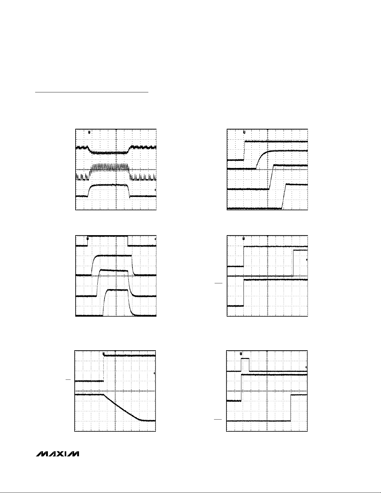
Typical Operating Characteristics (continued)
(V
IN1
= V
IN2
= 3.7V, PWR_ON = IN1, L = 2.2µH (LQH31CN2R2M53), CFF= 150pF, V
OUT1
= V
OUT2
= 2.6V, V
OUT3
= 1.867V (R1 =
150kΩ, R2 = 75kΩ), C
IN
= 10µF, C
BP
= 0.01µF, C
OUT1
= C
OUT2
= 4.7µF, C
OUT3
= 2.2µF, RESET pulled up with 100kΩ to OUT1,
T
A
= +25°C, unless otherwise noted.)
LOAD TRANSIENT (50mA TO 300mA)
MAX8620Y toc07
2µs/div
I
L
I
LOAD
V
OUT3
AC-COUPLED
50mV/div
200mA/div
300mA
50mA
200mA/div
POWER-UP WAVEFORMS
MAX8620Y toc08
40µs/div
V
OUT3
V
OUT1
V
OUT2
V
IN
2V/div
1V/div
1V/div
1V/div
PWR_ON STARTUP/SHUTDOWN WAVEFORMS
MAX8620Y toc09
100µs/div
V
OUT3
V
OUT1
V
OUT2
V
PWR_ON
2V/div
1V/div
1V/div
1V/div
RESET WAVEFORMS
MAX8620Y toc10
10ms/div
V
OUT1
V
PWR_ON
2V/div
1V/div
1V/div
V
RESET
OUT2 SHUTDOWN WAVEFORMS
MAX8620Y toc11
200µs/div
V
OUT2
V
EN2
1V/div
1V/div
HF_PWR STARTUP WAVEFORMS
MAX8620Y toc12
10ms/div
V
OUT1
V
HF_PWR
1V/div
2V/div
1V/div
V
RESET
Page 6

MAX8620Y
µPMIC for Microprocessors or DSPs
in Portable Equipment
6 _______________________________________________________________________________________
Typical Operating Characteristics (continued)
(V
IN1
= V
IN2
= 3.7V, PWR_ON = IN1, L = 2.2µH (LQH31CN2R2M53), CFF= 150pF, V
OUT1
= V
OUT2
= 2.6V, V
OUT3
= 1.867V (R1 =
150kΩ, R2 = 75kΩ), C
IN
= 10µF, C
BP
= 0.01µF, C
OUT1
= C
OUT2
= 4.7µF, C
OUT3
= 2.2µF, RESET pulled up with 100kΩ to OUT1,
T
A
= +25°C, unless otherwise noted.)
OUT1/OUT2 VOLTAGE vs. INPUT VOLTAGE
2.80
2.75
2.70
2.65
2.60
2.55
2.50
OUTPUT VOLTAGE (V)
2.45
2.40
2.35
2.30
3.0 5.5
OUT1/OUT2 LOAD REGULATION vs. LOAD CURRENT
-0.1
-0.3
-0.5
-0.7
-0.9
LOAD REGULATION (%)
-1.1
-1.3
-1.5
0 300
I
= 0mA
LOAD
I
= 300mA
LOAD
INPUT VOLTAGE (V)
LOAD CURRENT (mA)
DROPOUT VOLTAGE vs. LOAD CURRENT
400
MAX8620Y toc13
5.04.54.03.5
350
300
250
200
150
DROPOUT VOLTAGE (mV)
100
V
50
0
0 300
LOAD CURRENT (mA)
OUT_
MAX8620Y toc14
= 3V
25020050 100 150
OUT1/OUT2 POWER-SUPPLY
RIPPLE REJECTION vs. FREQUENCY
80
MAX8620Y toc15
25020015010050
70
60
50
40
30
20
10
POWER-SUPPLY RIPPLE REJECTION (dB)
0
0.1 1000
FREQUENCY (kHz)
100101
MAX8620Y toc16
Page 7

MAX8620Y
µPMIC for Microprocessors or DSPs
in Portable Equipment
_______________________________________________________________________________________ 7
Pin Description
PIN NAME FUNCTION
1 SEL1
2 SEL2
3 EN2
4 RESET
5BP
6 HF_PWR
7 PWR_ON
8FB
9 GND Ground. Connect GND to the exposed pad.
10 LX
11 IN2 Power Input 2. Connect IN2 to IN1 as close to the device as possible.
12 IN1
13 OUT1
14 OUT2
EP EP Exposed Pad. Connect EP to GND.
LDO Output-Voltage Select Input 1. SEL1 and SEL2 set the OUT1 and OUT2 voltages to one of nine
combinations (Table 1).
LDO Output-Voltage Select Input 2. SEL1 and SEL2 set the OUT1 and OUT2 voltages to one of nine
combinations (Table 1).
OUT2 Enable Input. Drive EN2 low to enable OUT2. Drive EN2 high to disable OUT2. If the MAX8620Y
is placed into shutdown (PWR_ON = HF_PWR = low), OUT2 does not power regardless of the status
of EN2 (Table 2, Figure 4).
Open-Drain, Active-Low Reset Output. RESET asserts low when V
regulation. RESET remains asserted for t
also asserts when OUT1 is disabled (Figure 4). RESET deasserts if OUT1 is enabled and V
above 87% of regulation after t
Reference Bypass Capacitor Node. Bypass BP with a 0.01µF capacitor to GND. BP is high
impedance when the MAX8620Y is disabled (PWR_ON = HF_PWR = low).
Hands-Free Enable Input. Drive HF_PWR high or apply a pulse to enable the MAX8620Y. Power is
enabled for 1.31s (typ) following a rising edge at HF_PWR (Table 2, Figure 4).
Power-Enable Input. Drive PWR_ON high to enable the MAX8620Y (Table 2, Figure 4). Drive PWR_ON
low to enter shutdown mode. In shutdown, the LX node is high impedance and both LDOs are
disabled (depending on the state of HF_PWR).
Step-Down Converter Output-Voltage Feedback Input. V
center of an external resistor-divider between LX and GND to set V
the Setting the Step-Down Output Voltage (OUT3) section).
Inductor Connection. LX is internally connected to the drain of the internal p-channel power MOSFET
and the drain of the n-channel synchronous rectifier. LX is high impedance when OUT3 is disabled.
Power Input 1. Connect IN1 to IN2 as close to the device as possible. Bypass IN1 to GND with a 10µF
ceramic capacitor, as close to the device as possible.
300mA LDO Output 1. Bypass OUT1 to GND with a 4.7µF ceramic capacitor for 300mA applications,
or a 2.2µF ceramic capacitor for 150mA applications. OUT1 is high impedance when disabled.
300mA LDO Output 2. Bypass OUT2 to GND with a 4.7µF ceramic capacitor for 300mA applications,
or a 2.2µF ceramic capacitor for 150mA applications. OUT2 is high impedance when disabled.
RP
.
after V
RP
rises above 87% (typ) of regulation. RESET
OUT1
FB
OUT1
regulates to 0.6V (typ). Connect FB to the
drops below 87% (typ) of
between 0.6V and 3.3V (see
OUT3
OUT1
is
Page 8
MAX8620Y
µPMIC for Microprocessors or DSPs
in Portable Equipment
8 _______________________________________________________________________________________
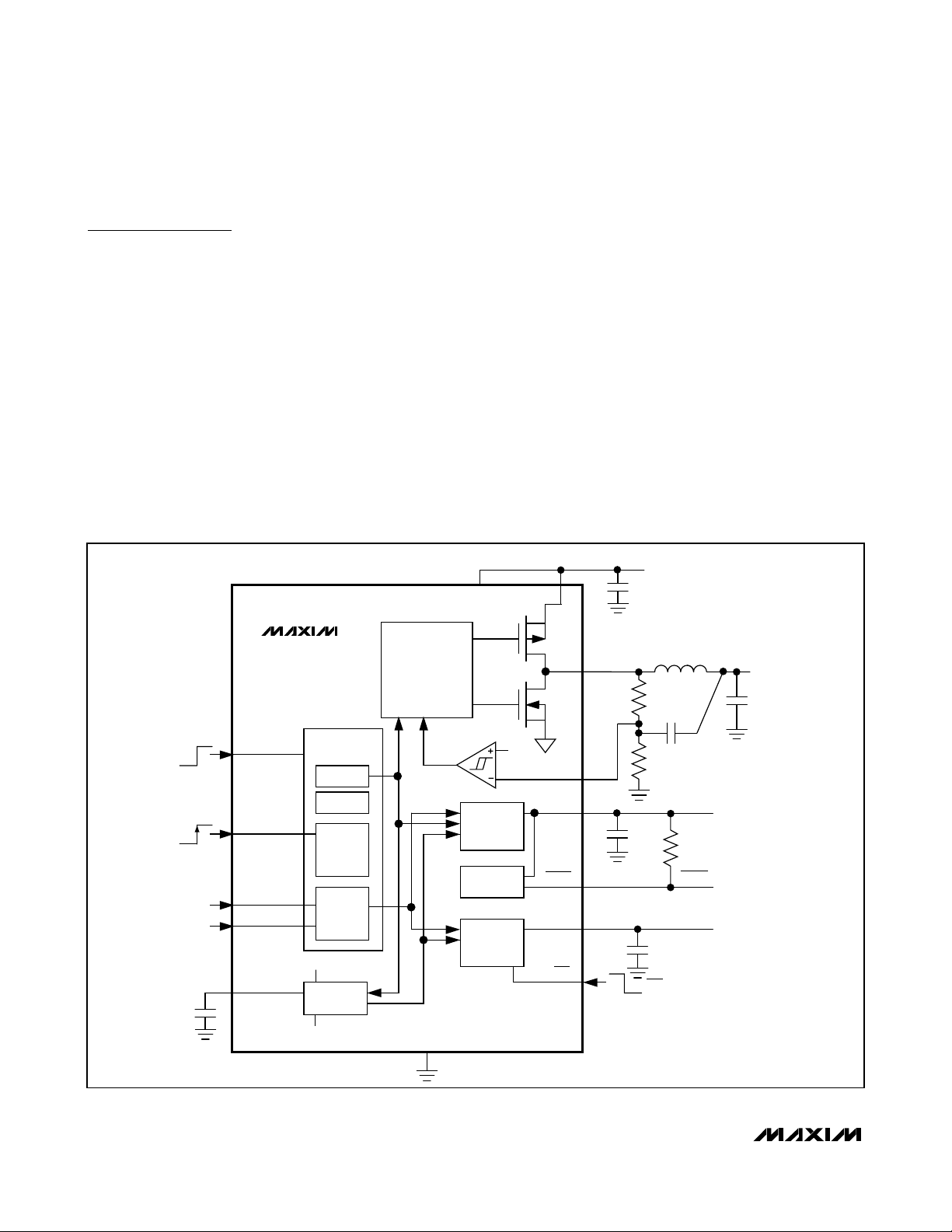
Detailed Description
The MAX8620Y µPMIC is designed to power low-corevoltage microprocessors or DSPs in portable devices.
The µPMIC contains a fixed-frequency, high-efficiency
step-down converter; two low-dropout regulators
(LDOs); a 30ms (min) reset timer; and power-on/off
control logic (Figure 1).
Step-Down DC-DC Control Scheme
The MAX8620Y step-down converter is optimized for
high-efficiency voltage conversion over a wide load
range while maintaining excellent transient response,
minimizing external component size, and minimizing
output voltage ripple. The DC-DC converter (OUT3)
also features an optimized on-resistance internal
MOSFET switch and synchronous rectifier to maximize
efficiency. The MAX8620Y utilizes a proprietary hysteretic-PWM control scheme that switches with nearly
fixed frequency up to 4MHz, allowing for ultra-small
external components. The step-down converter output
current is guaranteed up to 500mA.
When the step-down converter output voltage falls
below the regulation threshold, the error comparator
begins a switching cycle by turning the high-side pFET
switch on. This switch remains on until the minimum ontime (t
ON
) expires and the output voltage is in regula-
tion or the current-limit threshold (I
LIM3P
) is exceeded.
Once off, the high-side switch remains off until the minimum off-time (t
OFF
) expires and the output voltage
again falls below the regulation threshold. During this
off period, the low-side synchronous rectifier turns on
and remains on until either the high-side switch turns
on or the inductor current reduces to the rectifier-off
current threshold (I
LXOFF
= 30mA (typ)). The internal
synchronous rectifier eliminates the need for an external Schottky diode.
Figure 1. Functional Diagram
MAX8620Y
PWR_ON
CONTROL
LOGIC
ENABLE
STEP-DOWN
CONVERTER
CONTROL
V
IN
C
IN1
IN2
pFET
LX
nFET
0.6V
FB
IN
L
R1
C
FF
R2
OUT3
C
OUT3
UVLO
HF_PWR
SEL1
SEL2
BP
C
BP
ONE-
SHOT
TIMER
OUTPUT-
VOLTAGE
SELECT
IN1
REFERENCE
GND
GND
LDO1
CONTROL
RESET
LDO2
CONTROL
OUT1
RESET
OUT2
EN2
C
OUT1
EN2
C
OUT2
OUT1
R
PU
RESET
OUT2
Page 9

Voltage-Positioning Load Regulation
As seen in Figure 2, the MAX8620Y uses a unique step-
down converter feedback network. By taking feedback
from the LX node through R1, the usual phase lag due
to the output capacitor is removed, making the loop
exceedingly stable and allowing the use of a very small
ceramic output capacitor. This configuration causes the
output voltage to shift by the inductor series resistance
multiplied by the load current. This output-voltage shift
is known as voltage-positioning load regulation.
Voltage-positioning load regulation greatly reduces
overshoot during load transients, which effectively
halves the peak-to-peak output-voltage excursions
compared to traditional step-down converters. See the
Load-Transient Response graph in the Typical
Operating Characteristics section.
Two low-dropout, low-quiescent-current, high-accuracy
linear regulators supply loads up to 300mA each. The
LDO output voltages are set using SEL1 and SEL2 (see
Table 1). As shown in Figure 3, the LDOs include an
internal reference, error amplifiers, p-channel pass transistors, internal-programmable voltage-dividers, and an
OUT1 power-good comparator. Each error amplifier
compares the reference voltage to a feedback voltage
and amplifies the difference. If the feedback voltage is
lower than the reference voltage, the pass-transistor
gate is pulled lower, allowing more current to pass to
the outputs and increasing the output voltage. If the
feedback voltage is too high, the pass-transistor gate is
pulled up, allowing less current to pass to the output.
MAX8620Y
µPMIC for Microprocessors or DSPs
in Portable Equipment
_______________________________________________________________________________________ 9
Figure 2. Typical MAX8620Y DSP or µP Application
Table 1. MAX8620Y Output-Voltage
Selection
OUT1
RESET
LX
FB
OUT2
EN2
PWR_ON
GND
V
CELL
BATT
Li+
POWER-ON
KEY
C
IN
10µF
1MΩ
C
BP
0.01µF
IN2
IN1
MAX8620Y
BP
SEL2
SEL1
HF_PWR
SEL1 SEL2 OUT1 OUT2
IN1 IN1 3.00V 2.50V
IN1 OPEN 2.85V 2.85V
IN1 GND 3.00V 3.00V
OPEN IN1 3.30V 2.50V
OPEN OPEN 2.80V 2.60V
OPEN GND 3.30V 1.80V
GND IN1 2.85V 2.60V
GND OPEN 2.60V 2.60V
GND GND 1.80V 2.60V
2.6V
300mA
OUT3,
500mA
2.6V
300mA
I/O
RESET IN
CORE
DSP
OR
µP
ANALOG
ON/OFF
C
OUT1
4.7µF
R1
150kΩ
C
OUT2
4.7µF
R2
75kΩ
2.2µH
C
FF
150pF
L
100kΩ
C
OUT3
2.2µF
Page 10

MAX8620Y
LDO Output-Voltage
Selection (SEL1, SEL2)
As shown in Table 1, the LDO output voltages, OUT1
and OUT2, are set according to the logic states of
SEL1 and SEL2. SEL1 and SEL2 are trilevel inputs: IN1,
open, and GND. The input voltage, V
IN1
, must be a
dropout voltage (VDO) greater than the selected OUT1
and OUT2 voltages.
Power-Enable Input (PWR_ON)
Drive PWR_ON low to place the MAX8620Y in powerdown mode and reduce supply current to 5.5µA (typ).
Connect PWR_ON to IN1 = IN2 or logic-high to enable
the MAX8620Y. EN2 enables and disables OUT2 when
PWR_ON is high (Table 2). OUT1, OUT2, and OUT3 are
all disabled when PWR_ON is low. HF_PWR can temporarily bring the MAX8620 out of power-down mode
when PWR_ON is low (see the HF_PWR section). In
power-down, the control circuitry, internal-switching pchannel MOSFET, and the internal synchronous rectifier
(n-channel MOSFET) turn off, and LX becomes high
impedance. In addition, both LDOs are disabled.
OUT2 Enable (
EN2
)
Drive EN2 low to enable OUT2. Drive EN2 high to disable OUT2. If the MAX8620Y is placed into powerdown using PWR_ON (PWR_ON = low), OUT2 does not
power regardless of the status of EN2 (Table 2).
µPMIC for Microprocessors or DSPs
in Portable Equipment
10 ______________________________________________________________________________________
Figure 3. Linear-Regulator Functional Diagram
IN1
MAX8620Y
PWR_ON
HF_PWR
EN2
BP
GND
ON/OFF
LOGIC
LDO THERMAL
SENSOR
1.25V
REF
87%
REGULATION
ERROR-
AMP 2
ERROR-
AMP 1
POK
MOS DRIVER
WITH I
LIMIT
MOS DRIVER
WITH I
LIMIT
TIMER
P
OUT2
P
OUT1
RESET
Page 11

Hands-Free Enable Input (HF_PWR)
A rising edge at HF_PWR generates an internal oneshot pulse that enables the MAX8620Y for 1.31s (tHF). If
HF_PWR remains high after tHFexpires, the MAX8620Y
reenters shutdown. During t
HF
,
OUT3 and OUT1 are
enabled so the microprocessor (µP) can initialize and
assert a logic-high at PWR_ON. OUT2 enables during
tHFif EN2 is low. Once PWR_ON is high, the status of
HF_PWR is ignored. If PWR_ON remains low after t
HF
expires, the MAX8620Y reenters shutdown.
Power-Supply Sequencing
The step-down converter output (OUT3) always powers
up first and powers down last (Figure 4). OUT1 powers
approximately 70µs after OUT3, and OUT2 powers
approximately 50µs after V
OUT1
reaches 87% (typ) of
its regulation voltage. When PWR_ON goes low, OUT1
turns off, then OUT2 turns off, then OUT3 turns off 50µs
after PWR_ON goes low.
MAX8620Y
µPMIC for Microprocessors or DSPs
in Portable Equipment
______________________________________________________________________________________ 11
Figure 4. MAX8620Y Power-Supply Sequencing
Table 2. MAX8620Y Power Modes
*A rising edge at HF_PWR initiates a 1.31s one-shot timer. The status of HF_PWR shown in Table 2 indicates whether the one-shot
period has expired as follows:
1 = During t
HP
0 = tHPhas expired
PWR_ON HF_PWR* EN2 OUT1 AND OUT3 OUT2
1 X 1 Enabled Disabled
1 X 0 Enabled Enabled
0 1 1 Enabled Disabled
0 1 0 Enabled Enabled
0 0 X Disabled Disabled
HF_PWR
PWR_ON
OUT3
OUT1
OUT2
RESET
EN2
t
SU1
V
THR
t
SU2
t
RP
50µs
t
HF
Page 12

MAX8620Y
Reset Output (
RESET
)
RESET is an open-drain, active-low output that indicates the status of OUT1. RESET is typically pulled up
through a 100kΩ resistor to the system logic voltage.
RESET asserts at power-up. The reset timer begins
once V
OUT1
reaches 87% of regulation. RESET
deasserts 60ms after V
OUT1
rises above 87% (typ) of
regulation (see the Typical Operating Characteristics).
RESET also asserts when OUT1 is disabled.
Reference Bypass Capacitor Node (BP)
An optional 0.01µF bypass capacitor at BP creates a
lowpass filter for LDO noise reduction. OUT1 and OUT2
exhibit 45µV
RMS
of output-voltage noise with CBP=
0.01µF and C
OUT1
= C
OUT2
= 4.7µF.
Undervoltage Lockout
V
IN1
= V
IN
2
must exceed the 2.85V typical undervolt-
age-lockout threshold (V
UVLO
) before the MAX8620Y
enables OUT3 to begin power-supply sequencing (see
the Power-Supply Sequencing section). The UVLO
threshold hysteresis is typically 0.5V.
Current Limiting
The MAX8620Y 300mA LDOs limit their output current to
I
LIM_
= 550mA (typ). If the LDO output current exceeds
I
LIM_
, the corresponding LDO output voltage drops. The
step-down converter limits I
LIM3P
to 675mA (min).
Thermal-Overload Protection
Thermal-overload protection limits total power dissipation in the MAX8620Y. Independent thermal-protection
circuits monitor the step-down converter and the linearregulator circuits. When the MAX8620Y junction temperature exceeds TJ= +160°C, the thermal-overload
protection circuit disables the corresponding circuitry,
allowing the IC to cool. The thermal-overload protection
circuitry enables the MAX8620Y after the junction temperature cools by 15°C, resulting in a pulsed output during continuous thermal-overload conditions. Thermaloverload protection safeguards the MAX8620Y in the
event of fault conditions. For continuous operation, do
not exceed the absolute-maximum junction-temperature rating of T
J
= +150°C.
Applications Information
Power-On Closed-Loop System
When the MAX8620Y is used in conjunction with a
microcontroller, HF_PWR and PWR_ON can implement
a short-key power-on closed-loop system (Figure 5).
The MAX8620Y detects a rising edge at HF_PWR and
generates an internal 1.31s (typ) one-shot pulse that
begins power sequencing and temporarily enables
OUT1, OUT2, and OUT3 (depending on the state of
EN2). The 1.31s of power provides time for the processor to initialize and assert a logic-high at PWR_ON.
Once PWR_ON is driven high, OUT3, OUT1, and OUT2
(depending on the state of EN2) remain enabled. If the
microcontroller does not drive PWR_ON high during
tHF, the MAX8620Y disables OUT1, OUT2, and OUT3,
and reenters shutdown.
µPMIC for Microprocessors or DSPs
in Portable Equipment
12 ______________________________________________________________________________________
Figure 5. Short-Key Power-On Closed-Loop System
V
POWER-ON
KEY
1MΩ
MAX8620Y
HF_PWR
PWR_ON
POWER-HOLD SIGNAL
V
V
CORE
I/O
ANA
µP
PWR HOLD
Page 13

If a long-key press is preferred, see Figure 6. PWR_ON
must remain high until a microprocessor asserts a logichigh signal when using this circuit. If a system includes
multiple power-on sources, use a diode OR configuration, as shown in Figure 7.
Setting the Step-Down Output Voltage
(OUT3)
Select a step-down converter output voltage between
0.6V and 3.3V by connecting a resistor voltage-divider
between LX, FB, and GND (see Figure 2). The FB bias
current, I
FB
, is typically 10nA. Select R2 so the resistordivider bias current dominates IFBby a factor of 10. A
wide range of resistor values is acceptable, but a good
starting point is to choose R2 = 100kΩ. R1 is given by:
where V
FB
= 0.6V.
V
OUT3
can be set between 0.6V and 3.3V, but the stepdown converter dropout voltage and inductor voltage
drop impact how close V
OUT3
can be to V
IN2
. Total
dropout voltage is a function of the pFET on-resistance,
the DCR of the inductor, and the load as follows:
For example, with 300mA load:
As a result, V
IN1
= V
IN2
must exceed the desired
V
OUT3
by 210mV to maintain regulation.
Inductor Selection
The MAX8620Y step-down converter operates with inductors between 1µH and 4.7µH. Low inductance values are
physically smaller but require faster switching, which
results in some efficiency loss. See the Typical Operating
Characteristics section for efficiency and switching frequency versus inductor value plots. The inductor’s DC
current rating needs to be only 100mA greater than the
application’s maximum load current because the
MAX8620Y step-down converter features zero-current
overshoot during startup and load transients.
For output voltages above 2.0V, when light-load efficiency is important, the minimum recommended inductor is 2.2µH. For optimum voltage-positioning load
transients, choose an inductor with DC series resistance in the 50mΩ to 150mΩ range (Table 3). For higher efficiency at heavy loads (above 200mA) or minimal
load regulation (but some transient overshoot), the
resistance should be kept below 100mΩ. For light-load
applications up to 200mA, much higher resistance is
acceptable with very little impact on performance.
MAX8620Y
µPMIC for Microprocessors or DSPs
in Portable Equipment
______________________________________________________________________________________ 13
Figure 6. Long-Key Power-On Closed Loop
Figure 7. Multiple Power-On Inputs
V
POWER-ON
KEY
1MΩ
AC ADAPTER
HANDS-FREE KIT
POWER-ON
KEY
1MΩ
MAX8620Y
PWR_ON
POWER-HOLD SIGNAL
MAX8620Y
HF_PWR
PWR_ON
POWER-HOLD SIGNAL
V
V
CORE
I/O
ANA
V
V
V
CORE
I/O
ANA
µP
PWR HOLD
µP
PWR HOLD
⎛
V
OUT
⎜
V
⎝
RR
12 1
=
FB
⎞
3
−
⎟
⎠
V I R DCR
OUT DO OUT ONP INDUCTOR33()
=×+
()
VmAmmV
OUT DO3
300 0 65 50 210
()
.=×+
()
=ΩΩ
Page 14
MAX8620Y
µPMIC for Microprocessors or DSPs
in Portable Equipment
14 ______________________________________________________________________________________
Table 3. Suggested Inductors
MANUFACTURER SERIES
LB2012
INDUCTANCE
(µH)
1.0
2.2
ESR
(Ω)
0.15
0.23
CURRENT RATING
(mA)
300
240
DIMENSIONS (mm)
2.0 x 1.25 x 1.25
= 3.1mm
3
Taiyo Yuden
Murata
TOKO
LB2016
LB2518
LBC2518
CB2012
CB2016
CB2518
LQH32C_53
LQM43FN
D310F
D312C
1.0
1.5
2.2
3.3
1.0
1.5
2.2
3.3
1.0
1.5
2.2
3.3
4.7
2.2
4.7
2.2
4.7
2.2
4.7
1.0
2.2
4.7
2.2
4.7
1.5
2.2
3.3
1.5
2.2
2.7
3.3
0.09
0.11
0.13
0.20
0.06
0.07
0.09
0.11
0.08
0.11
0.13
0.16
0.20
0.23
0.40
0.13
0.25
0.09
0.13
0.06
0.10
0.15
0.10
0.17
0.13
0.17
0.19
0.10
0.12
0.15
0.17
455
350
315
280
500
400
340
270
775
660
600
500
430
410
300
510
340
510
340
1000
790
650
400
300
1230
1080
1010
1290
1140
980
900
2.0 x 1.6 x 1.8
= 5.8mm
2.5 x 1.8 x 2.0
= 9mm
2.5 x 1.8 x 2.0
= 9mm
2.0 x 1.25 x 1.25
= 3.1mm
2.0 x 1.6 x 1.8
= 5.8mm
2.5 x 1.8 x 2.0
= 9mm
3.2 x 2.5 x 1.7
= 14mm
4.5 x 3.2 x 0.9
= 13mm
3.6 x 3.6 x 1.0
= 13mm
3.6 x 3.6 x 1.2
= 16mm
3
3
3
3
3
3
3
3
3
3
Sumida CDRH2D11
1.5
2.2
3.3
4.7
0.05
0.08
0.10
0.14
900
780
600
500
3.2 x 3.2 x 1.2
= 12mm
3
Page 15

MAX8620Y
µPMIC for Microprocessors or DSPs
in Portable Equipment
______________________________________________________________________________________ 15
Capacitor Selection
Step-Down Converter Output Capacitor
The output capacitor, C
OUT3
, is required to keep the
output voltage ripple small and to ensure regulation
loop stability. C
OUT3
must have low impedance at the
switching frequency. Ceramic capacitors with X5R or
X7R dielectric are highly recommended due to their
small size, low ESR, and small temperature coefficients.
Due to the unique feedback network, the output capacitance can be very low. For most applications, a 2.2µF
capacitor is sufficient. For optimum load-transient performance and very low output ripple, the output capacitor value in µFs should be equal to or larger than the
inductor value in µHs.
Input Capacitor
The input capacitor, CIN, reduces the current peaks
drawn from the battery or input power source and
reduces switching noise in the IC. The impedance of
CINat the switching frequency should be kept very low.
Ceramic capacitors with X5R or X7R dielectrics are
highly recommended due to their small size, low ESR,
and small temperature coefficients. Use a 10µF ceramic capacitor or equivalent amount of multiple capacitors
in parallel between IN1 and GND. Connect CINas
close as possible to the MAX8620Y to minimize the
impact of PC board trace inductance.
Feed-Forward Capacitor
The feed-forward capacitor, CFF, sets the feedback
loop response, controls the switching frequency, and is
critical in obtaining the best efficiency possible.
Choose a small ceramic C0G (NPO) or X7R capacitor
with a value given by:
where R1 is the resistor between LX and FB (Figure 2).
Select the closest standard value to C
FF
as possible.
LDO Output Capacitors
For applications that require greater than 150mA of output current, connect a 4.7µF ceramic capacitor
between the LDO output and GND. For applications
that require less than 150mA of output current, connect
a 2.2µF ceramic capacitor between the LDO output
and GND. The LDO output capacitor’s (C
OUT_
) equiva-
lent series resistance (ESR) affects stability and output
noise. Use output capacitors with an ESR of 0.1Ω or
less to ensure stability and optimum transient response.
Surface-mount ceramic capacitors have very low ESR
and are commonly available in values up to 10µF.
Connect C
OUT
as close as possible to the MAX8620Y
to minimize the impact of PC board trace inductance.
Power Dissipation and Thermal
Considerations
The MAX8620Y total power dissipation, PD, is estimated using the following equations:
`
where P
IN(OUT3)
is the input power for OUT3, η is the
step-down converter efficiency, and R
DC(INDUCTOR)
is
the inductor’s DC resistance.
The die junction temperature can be calculated as follows:
where θJA= 55°C/W at +70°C.
TJshould not exceed +150°C in normal operating conditions.
PC Board Layout and Routing
High switching frequencies and relatively large peak
currents make the PC board layout a very important
aspect of design. Good design minimizes excessive
EMI on the feedback paths and voltage gradients in the
ground plane, both of which can result in instability or
regulation errors. Connect CINclose to IN1 and GND.
Connect the inductor and output capacitors (C
OUT3
) as
close to the IC as possible and keep the traces short,
direct, and wide.
The traces between C
OUT3
, CFF, and FB are sensitive
to inductor magnetic-field interference. Route these
traces between ground planes or keep the traces away
from the inductor.
L
C
=×110
FF
S
R
PP P P
=+ +
D LOSS OUT LOSS OUT LOSS OUT
PP I
LOSS OUT IN OUT OUT
() () ()
12 3
PIVV
LOSS OUT OUT IN OUT
PIVV
LOSS OUT OUT IN OUT
() () ()
()()
33 3
=
11 1
=
()()
22 2
=
R
×
DC
⎛
1
⎜
⎝
(()INDUCTOR
−
()
−
()
η
⎞
−−
⎟
⎠
100
2
TTP
=+×θ
JADJA
Page 16

MAX8620Y
Connect GND to the ground plane. The external feedback network should be very close to the FB pin, within
0.2in (5mm). Keep noisy traces, such as the LX node,
as short as possible. Connect GND to the exposed
paddle directly under the IC. Figure 8 and the
MAX8620Y evaluation kit illustrate examples of PC
board layout and routing schemes.
µPMIC for Microprocessors or DSPs
in Portable Equipment
16 ______________________________________________________________________________________
Figure 8. Recommended PC Board Layout
Chip Information
TRANSISTOR COUNT: 4481
PROCESS: BiCMOS
MAX8620Y
15432
SEL2
RESET
6
91011121314
SEL1
EN2
HF_PWR
7
PWR_ON
BP
OUT1
IN2
OUT2
IN1
GND
8
FB
LX
TOP VIEW
3mm x 3mm x 0.8mm
TDFN
Pin Configuration
OUT2
SEL1SEL1
SEL2SEL2
EN2EN2
RESET
HF_PWR
PWR_ON
C3
U1
C6
R2
C5
C2
C1
R1 L1
OUT1
IN
GND
C4
OUT3
Page 17

MAX8620Y
µPMIC for Microprocessors or DSPs
in Portable Equipment
______________________________________________________________________________________ 17
Package Information
(The package drawing(s) in this data sheet may not reflect the most current specifications. For the latest package outline information
go to www.maxim-ic.com/packages
.)
PIN 1
INDEX
AREA
D
E
A1
A
A2
DETAIL A
N
b
E2
C
L
L
D2
0.35x0.35
PIN 1 ID
[(N/2)-1] x e
REF.
e
k
C
L
L
6, 8, &10L, DFN THIN.EPS
-DRAWING NOT TO SCALE-
e
PACKAGE OUTLINE, 6,8,10 & 14L,
TDFN, EXPOSED PAD, 3x3x0.80 mm
21-0137
e
1
G
2
Page 18

MAX8620Y
µPMIC for Microprocessors or DSPs
in Portable Equipment
Maxim cannot assume responsibility for use of any circuitry other than circuitry entirely embodied in a Maxim product. No circuit patent licenses are
implied. Maxim reserves the right to change the circuitry and specifications without notice at any time.
18 ____________________Maxim Integrated Products, 120 San Gabriel Drive, Sunnyvale, CA 94086 408-737-7600
© 2005 Maxim Integrated Products Printed USA is a registered trademark of Maxim Integrated Products, Inc.
Package Information (continued)
(The package drawing(s) in this data sheet may not reflect the most current specifications. For the latest package outline information
go to www.maxim-ic.com/packages
.)
COMMON DIMENSIONS
SYMBOL
A
D
E
A1
L
A2 0.20 REF.
MIN. MAX.
0.70 0.80
2.90 3.10
2.90 3.10
0.00 0.05
0.20 0.40
0.25 MIN.k
PACKAGE VARIATIONS
PKG. CODE
T633-2 6 1.50±0.10 2.30±0.10 0.95 BSC
T833-2 8 1.50±0.10 2.30±0.10
T833-3 8 1.50±0.10 2.30±0.10
-DRAWING NOT TO SCALE-
N
D2 E2 e
2.30±0.101.50±0.106T633-1 0.95 BSC MO229 / WEEA 1.90 REF0.40±0.05
1.50±0.10
1.50±0.10
1.70±0.10 2.30±0.1014T1433-1
2.30±0.108T833-1
2.30±0.1010T1033-1
JEDEC SPEC
MO229 / WEEA
0.65 BSC
0.65 BSC MO229 / WEEC
0.65 BSC MO229 / WEEC
0.50 BSC
0.40 BSC
0.40 BSC
MO229 / WEEC
MO229 / WEED-3
- - - - 0.20±0.05 2.40 REFT1433-2 14 2.30±0.101.70±0.10
b
[(N/2)-1] x e
0.40±0.05 1.90 REF
1.95 REF0.30±0.05
0.30±0.05 1.95 REF
0.30±0.05 1.95 REF
2.00 REF0.25±0.05
2.40 REF0.20±0.05- - - -
DOWNBONDS
ALLOWED
NO
NO
NO
NO
YES
NO
YES
NO
PACKAGE OUTLINE, 6,8,10 & 14L,
TDFN, EXPOSED PAD, 3x3x0.80 mm
21-0137
2
G
2
 Loading...