

Page 1
General Description
The MAX8614A/MAX8614B dual-output step-up DC-DC
converters generate both a positive and negative supply voltage that are each independently regulated. The
positive output delivers up to 50mA while the inverter
supplies up to 100mA with input voltages between 2.7V
and 5.5V. The MAX8614A/MAX8614B are ideal for powering CCD imaging devices and displays in digital
cameras and other portable equipment.
The MAX8614A/MAX8614B generate an adjustable
positive output voltage up to +24V and a negative output down to 16V below the input voltage. The
MAX8614B has a higher current limit than the
MAX8614A. Both devices operate at a fixed 1MHz frequency to ease noise filtering in sensitive applications
and to reduce external component size.
Additional features include pin-selectable power-on
sequencing for use with a wide variety of CCDs, True
Shutdown™, overload protection, fault flag, and internal
soft-start with controlled inrush current.
The MAX8614A/MAX8614B are available in a spacesaving 3mm x 3mm 14-pin TDFN package and
are specified over the -40°C to +85°C extended
temperature range.
Applications
CCD Bias Supplies and OLED Displays
Digital Cameras
Camcorders and Portable Multimedia
PDAs and Smartphones
Features
♦ Dual Output Voltages (+ and -)
♦ Adjustable Up to +24V and Down to -10V at 5.5V
IN
♦ Output Short/Overload Protection
♦ True Shutdown on Both Outputs
♦ Controlled Inrush Current During Soft-Start
♦ Selectable Power-On Sequencing
♦ Up to 90% Efficiency
♦ 1µA Shutdown Current
♦ 1MHz Fixed-Frequency PWM Operation
♦ Fault-Condition Flag
♦ Thermal Shutdown
♦ Small, 3mm x 3mm, 14-Pin TDFN Package
MAX8614A/MAX8614B
Dual-Output (+ and -) DC-DC
Converters for CCD
________________________________________________________________ Maxim Integrated Products 1
19-4014; Rev 0; 3/06
For pricing, delivery, and ordering information, please contact Maxim/Dallas Direct! at
1-888-629-4642, or visit Maxim’s website at www.maxim-ic.com.
14 13 12 11 10
9
8
1
+
23
4567
LXN
VCCPVP
PGNDREF
AV
CC
FBN
ONBST
TOP VIEW
MAX8614A
MAX8614B
LXP
ONINV
SEQFBP
FLT
GND
TDFN
Pin Configuration
Typical Operating Circuit
Ordering Information
True Shutdown is a trademark of Maxim Integrated Products, Inc.
+Denotes lead-free package.
PART
MAX8614AETD+
MAX8614BETD+
INPUT
(2.7V TO 5.5V)
TEMP
RANGE
-40°C to
+85°C
-40°C to
+85°C
PINPACKAGE
14 TDFN
3mm x 3mm
(T1433-2)
14 TDFN
3mm x 3mm
(T1433-2)
TOP
MARK
ABG 0.44/0.33
ABH 0.8/0.75
ILIM
BST/INV
V
CC
ONINV
ONBST
AV
CC
MAX8614A
MAX8614B
REF
AV
CC
SEQ
FLT
GND PGND
LXN
FBN
PVP
LXP
FBP
V
-7.5V
V
+15V
INV
REF
BST
Page 2
MAX8614A/MAX8614B
Dual-Output (+ and -) DC-DC
Converters for CCD
2 _______________________________________________________________________________________
ABSOLUTE MAXIMUM RATINGS
Stresses beyond those listed under “Absolute Maximum Ratings” may cause permanent damage to the device. These are stress ratings only, and functional
operation of the device at these or any other conditions beyond those indicated in the operational sections of the specifications is not implied. Exposure to
absolute maximum rating conditions for extended periods may affect device reliability.
VCC, AVCCto GND...................................................-0.3V to +6V
LXN to V
CC
.............................................................
-18V to +0.3V
LXP to PGND ..........................................................-0.3V to +33V
REF, ONINV, ONBST, SEQ, FBN, FBP
FLT to GND..........................................-0.3V to (AV
CC
+ 0.3)V
PVP to GND................................................-0.3V to (V
CC
+ 0.3)V
AV
CC
to VCC..........................................................-0.3V to +0.3V
PGND to GND .......................................................-0.3V to +0.3V
Continuous Power Dissipation (T
A
= +70°C Multilayer Board)
14-Pin 3mm x 3mm TDFN (derate 18.2mW/°C above
T
A
= +70°C) ............................................................1454.4mW
Operating Temperature Range ...........................-40°C to +85°C
Junction Temperature......................................................+150°C
Storage Temperature Range .............................-65°C to +150°C
Lead Temperature (soldering, 10s) .................................+300°C
ELECTRICAL CHARACTERISTICS
(VCC= V
AVCC
= V
ONINV = VONBST
= 3.6V, PGND = SEQ = GND, C6 = 0.22µF, C1 = 2.2µF, C2 = 4.7µF, Figure 1, TA= 0°C to +85°C,
unless otherwise noted. Typical values are at T
A
= +25°C.)
AVCC and VCC Voltage Range (Note 1) 2.7 5.5 V
UVLO Threshold VCC rising 2.42 2.55 2.66 V
UVLO Hysteresis 25 mV
Step-Up Output Voltage Adjust Range V
PARAMETER CONDITIONS MIN TYP MAX UNITS
AVCC
24 V
Inverter Output Voltage Adjust Range V
LXP Current Limit
LXP Short-Circuit Current Limit
LXN Current Limit
LXN On-Resistance V
LXP On-Resistance V
PVP On-Resistance V
Maximum Duty Cycle Step-up and inverter 82 90 %
Quiescent Current (Switching, No Load)
Quiescent Current (No Switching, No Load)
Shutdown Supply Current
FBP Line Regulation V
FBN Line Regulation V
- VCC (Note 2) -16 0 V
INV
MAX8614B 0.7 0.8 0.9
MAX8614A 0.34 0.44 0.52
MAX8614B 0.90 1.05 1.20
MAX8614A 0.52 0.61 0.70
MAX8614B 0.65 0.75 0.85
MAX8614A 0.28 0.33 0.38
= 3.6V 0.6 1.1 Ω
CC
= 3.6V 0.625 Ω
CC
= 3.6V 0.15 0.3 Ω
CC
I
AVCC
I
VCC
I
AVCC
I
V
CC
T
= +25°C 0.1 5
A
T
= +85°C 0.1
A
= 2.7V to 5.5V -20 mV/D
CC
= 2.7V to 5.5V 20
CC
0.75 1.4
23
400 800
815
mA
µA
µA
mV/
(D - 0.5)
A
A
A
Page 3
MAX8614A/MAX8614B
Dual-Output (+ and -) DC-DC
Converters for CCD
_______________________________________________________________________________________ 3
ELECTRICAL CHARACTERISTICS (continued)
(VCC= V
AVCC
= V
ONINV = VONBST
= 3.6V, PGND = SEQ = GND, C6 = 0.22µF, C1 = 2.2µF, C2 = 4.7µF, Figure 1, TA= 0°C to +85°C,
unless otherwise noted. Typical values are at T
A
= +25°C.)
FBP Load Regulation
FBN Load Regulation
Oscillator Frequency 0.93 1 1.07 MHz
Soft-Start Interval Step-up and inverter 10 ms
Overload-Protection Fault Delay 100 ms
FBP, FBN, REFERENCE
REF Output Voltage No load 1.24 1.25 1.26 V
REF Load Regulation 0µA < I
REF Line Regulation 3.3V < V
FBP Threshold Voltage No load 0.995 1.010 1.025 V
FBN Threshold Voltage No load -10 0 +10 mV
FBP Input Leakage Current V
FBN Input Leakage Current FBN = -10mV
LXN Input Leakage Current V
LXP Input Leakage Current V
PVP Input Leakage Current V
FLT Input Leakage Current V
FLT Input Resistance Fault mode, T
ONINV, ONBST, SEQ LOGIC INPUTS
Logic-Low Input 2.7V < V
Logic-High Input 2.7V < V
Bias Current T
PARAMETER CONDITIONS MIN TYP MAX UNITS
I
= I
LXP
I
= I
LXP
I
= I
LXN
I
= I
LXN
FBP =
= -12V
LXN
= 23V
LXP
= 0V
PVP
= 3.6V
FLT
= +25°C 0.1 1 µA
A
, MAX8614B -15
ILIMMIN
, MAX8614A -35
ILIMMIN
, MAX8614B 17.5
ILIMMIN
, MAX8614A 65
ILIMMIN
< 50µA 10 mV
REF
< 5.5V 2 5 mV
AVCC
T
= +25°C -50 +5 +50
1.025V
= +25°C 10 20 Ω
A
< 5.5V 0.5 V
AVCC
< 5.5V 1.6 V
AVCC
A
T
= +85°C +5
A
T
= +25°C -50 +5 +50
A
T
= +85°C +5
A
T
= +25°C -5 +0.1 +5
A
T
= +85°C +0.1
A
T
= +25°C -5 +0.1 +5
A
T
= +85°C +0.1
A
T
= +25°C -5 +0.1 +5
A
T
= +85°C +0.1
A
T
= +25°C -1 +0.1 +1
A
T
= +85°C +0.1
A
mV/A
mV/A
nA
nA
µA
µA
µA
µA
Page 4
MAX8614A/MAX8614B
Dual-Output (+ and -) DC-DC
Converters for CCD
4 _______________________________________________________________________________________
ELECTRICAL CHARACTERISTICS
(VCC= V
AVCC
= V
ONINV = VONBST
= VEN= 3.6V, PGND = SEQ = GND, C6 = 0.22µF, C1 = 2.2µF, C2 = 6.7µF, Figure 1, TA= -40°C
to +85°C, unless otherwise noted.) (Note 3)
Note 1: Output current and on-resistance are specified at 3.6V input voltage. The IC operates to 2.7V with reduced performance.
Note 2: The specified maximum negative output voltage is referred to V
CC
, and not to GND. With VCC= 3.3V, the maximum negative
output is then -12.7V.
Note 3: Specifications to -40°C are guaranteed by design, not production tested.
A
= VCC Voltage Range (Note 1) 3 5.5 V
VCC
UVLO Threshold VCC rising 2.42 2.82 V
Step-Up Output Voltage Adjust Range V
Inverter Output Voltage Adjust Range V
LXP Current Limit
LXP Short-Circuit Current Limit
LXN Current Limit
LXN On-Resistance V
PVP On-Resistance V
Maximum Duty Cycle Step-up and inverter 82 %
Quiescent Current (Switching, No Load)
Quiescent Current (No Switching, No Load)
Oscillator Frequency 0.93 1.07 MHz
FBP, FBN, REFERENCE
REF Output Voltage No load 1.235 1.260 V
FBP Threshold Voltage No load 0.995 1.025 V
FBN Threshold Voltage No load -10 +10 mV
ONINV, ONBST SEQ LOGIC INPUTS
Logic-Low Input 2.7V < V
Logic-High Input 2.7V < V
PARAMETER CONDITIONS MIN TYP MAX UNITS
AVCC
- VCC (Note 2) -16 0 V
INV
MAX8614B 0.7 0.9
MAX8614A 0.34 0.52
MAX8614B 0.9 1.2
MAX8614A 0.52 0.70
MAX8614B 0.65 0.85
MAX8614A 0.28 0.38
= 3.6V 1.1 Ω
CC
= 3.6V 0.3 Ω
CC
I
AVCC
I
VCC
I
AVCC
I
VCC
< 5.5V 0.5 V
AVCC
< 5.5V 1.6 V
AVCC
24 V
1.4
3
800
15
A
A
A
mA
µA
Page 5
MAX8614A/MAX8614B
Dual-Output (+ and -) DC-DC
Converters for CCD
_______________________________________________________________________________________ 5
Typical Operating Characteristics
(TA= +25°C, VCC= V
AVCC
= 3.6V, SEQ = GND, Figure 1, unless otherwise noted.)
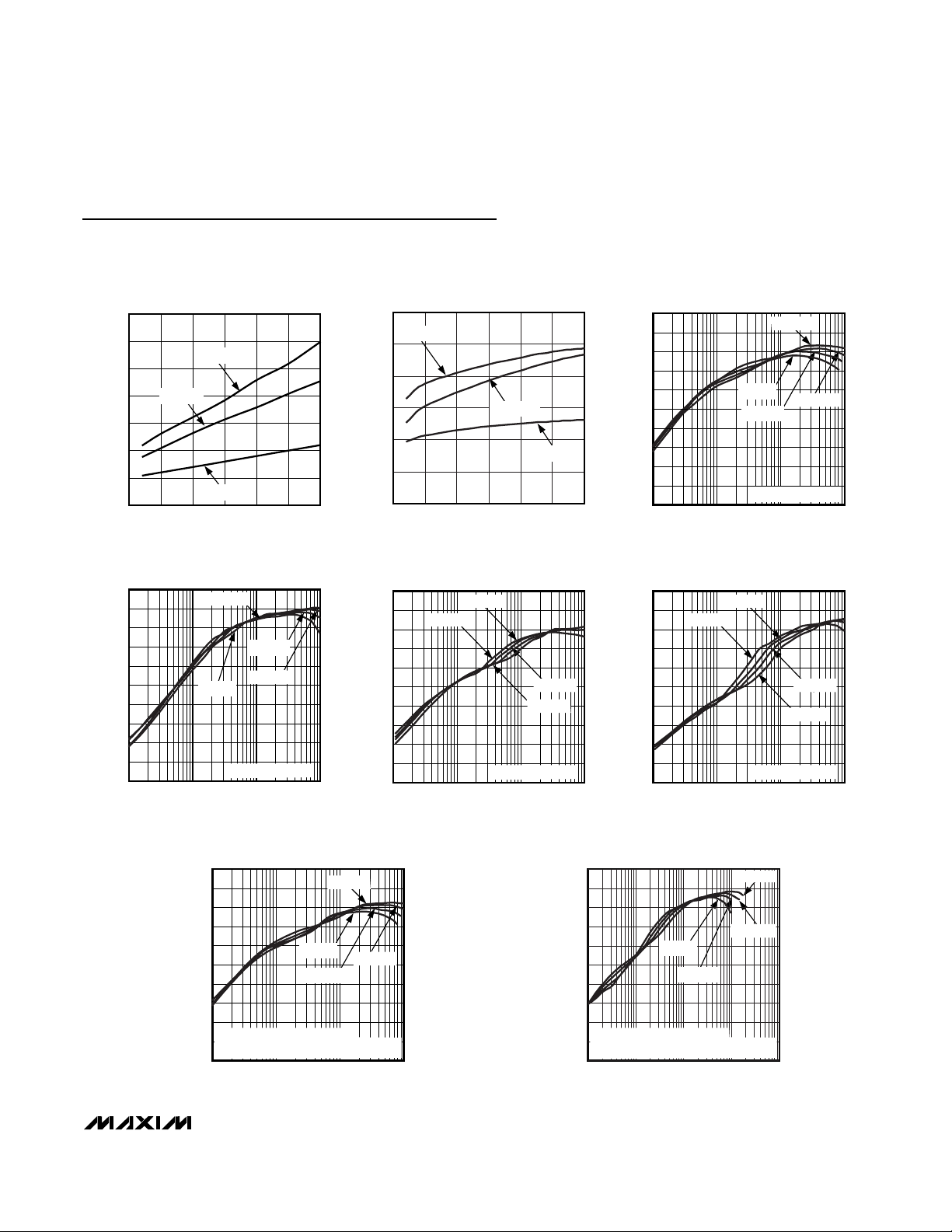
MAXIMUM OUTPUT CURRENT
vs. INPUT VOLTAGE
350
300
250
200
150
100
MAXIMUM OUTPUT CURRENT (mA)
50
0
2.5 3.0 3.5 4.0 4.5 5.0 5.5
V
V
= 15V
OUT
INPUT VOLTAGE (V)
= 10V
OUT
V
= 20V
OUT
POSITIVE OUTPUT EFFICIENCY
vs. OUTPUT CURRENT
100
90
80
70
60
50
40
EFFICIENCY (%)
30
20
10
0
0.1 1 10 100
VCC = 5V
VCC = 3V
OUTPUT CURRENT (mA)
MAXIMUM OUTPUT CURRENT
vs. INPUT VOLTAGE
V
= -5V
INV
V
= -7.5V
INV
V
INPUT VOLTAGE (V)
NEGATIVE OUTPUT EFFICIENCY
vs. OUTPUT CURRENT
VCC = 3.6V
VCC = 3V
VCC = 5V
L = 4.7µH, C = 4.7µF
OUTPUT CURRENT (mA)
VCC = 3.6V
VCC = 4.2V
L = 10µH, C = 10µF
300
250
MAX8614A/B toc01
200
150
100
50
MAXIMUM OUTPUT CURRENT (mA) .
0
2.5 3.0 3.5 4.0 4.5 5.0 5.5
100
90
80
MAX8614A/B toc04
70
60
50
40
EFFICIENCY (%)
30
20
10
0
0.1 1 10 100
= -10V
INV
VCC = 4.2V
MAX8614A/B toc02
EFFICIENCY (%)
MAX8614A/B toc05
EFFICIENCY (%)
POSITIVE OUTPUT EFFICIENCY
vs. OUTPUT CURRENT
100
90
80
70
60
50
40
30
20
10
0
0.1 1 10 100
OUTPUT CURRENT (mA)
VCC = 5V
VCC = 3V
VCC = 3.6V
L = 2.2µH, C = 2.2µF
VCC = 4.2V
NEGATIVE OUTPUT EFFICIENCY
vs. OUTPUT CURRENT
100
90
80
70
60
50
40
30
20
10
0
0.1 1 10 100
VCC = 3.6V
VCC = 3V
VCC = 4.2V
VCC = 5V
L = 10µH, C = 10µF
OUTPUT CURRENT (mA)
MAX8614A/B toc03
MAX8614A/B toc06
OUTPUT EFFICIENCY
vs. OUTPUT CURRENT
100
90
80
70
60
50
40
EFFICIENCY (%)
30
20
BOTH OUTPUTS LOADED EQUALLY
10
L1 = 2.2µH, C1 = 2.2µF, L2 = 4.7µH, C2 = 4.7µF
0
0.1 1 10 100
OUTPUT CURRENT (mA)
VCC = 5V
VCC = 3V
VCC = 3.6V
VCC = 4.2V
MAX8614A/B toc07
100
90
80
70
60
50
40
EFFICIENCY (%)
30
20
10
0
0.1 1 10 100 1000
OUTPUT EFFICIENCY
vs. OUTPUT CURRENT
VCC = 5V
VCC = 4.2V
VCC = 3V
VCC = 3.6V
BOTH OUTPUTS LOADED EQUALLY
L1 = 10µH, C1 = 10µF, L2 = 10µH, C2 = 10µF
OUTPUT CURRENT (mA)
MAX8614A/B toc08
Page 6
MAX8614A/MAX8614B
Dual-Output (+ and -) DC-DC
Converters for CCD
6 _______________________________________________________________________________________
Typical Operating Characteristics (continued)
(TA= +25°C, VCC= V
AVCC
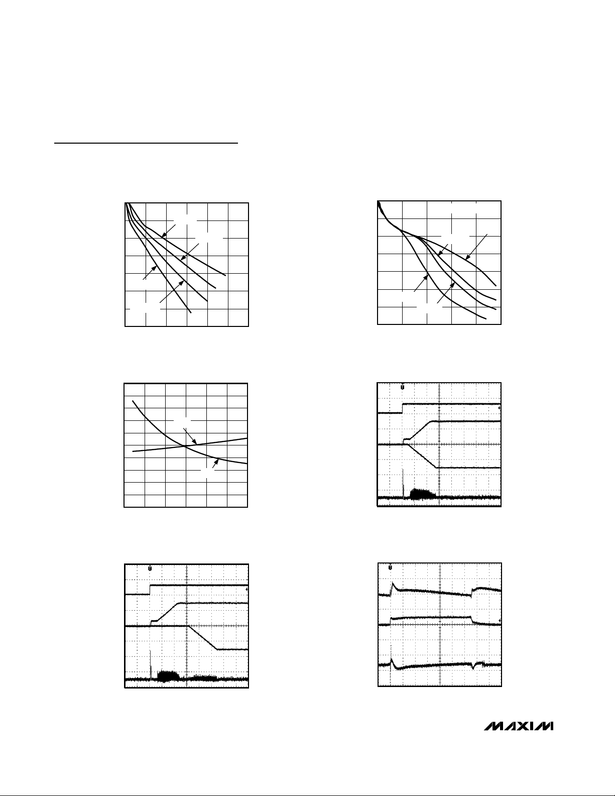
= 3.6V, SEQ = GND, Figure 1, unless otherwise noted.)
CHANGE IN OUTPUT VOLTAGE
vs. LOAD CURRENT (POSITIVE OUTPUT)
LOAD CURRENT (mA)
CHANGE IN OUTPUT VOLTAGE (%)
MAX8614A/B toc09
0 25 50 75 100 125 150
-3.5
-3.0
-2.5
-2.0
-1.5
-1.0
-0.5
0
VCC = 3V
VCC = 5V
VCC = 4.2V
VCC = 3.6V
CHANGE IN OUTPUT VOLTAGE
vs. OUTPUT CURRENT (NEGATIVE OUTPUT)
0
-0.5
-1.0
-1.5
-2.0
V
OUT
VIN = 4.2V
- = -7.5V
VIN = 5V
MAX8614A/B toc10
NO-LOAD SUPPLY CURRENT
1000
900
800
700
600
500
400
300
SUPPLY CURRENT (µA)
200
100
0
2.5 3.0 3.5 4.0 4.5 5.0 5.5
V
ONINV
V
ONBST
V
BST
V
INV
I
IN
vs. INPUT VOLTAGE
AV
CC
INPUT VOLTAGE (V)
SOFT-START WAVEFORMS
SEQ = AV
CC
4ms/div
V
CC
MAX8614A/B toc13
MAX8614A/B toc11
5V/div
0V
10V/div
0V
5V/div
100mA/div
0V
-2.5
CHANGE IN OUTPUT VOLTAGE (%)
-3.0
-3.5
VIN = 3V
0 25 50 75 100 125
SOFT-START WAVEFORMS
SEQ = GND
V
ONINV
V
ONBST
V
BST
V
INV
I
IN
V
BST
V
IN
3.5V TO 4.5V
TO 3.5V
V
INV
VIN = 3.6V
OUTPUT CURRENT (mA)
4ms/div
LINE TRANSIENT
40µs/div
MAX8614A/B toc12
MAX8614A/B toc14
5V/div
0V
10V/div
0V
5V/div
100mA/div
0V
50mV/div
AC-COUPLED
3.5V
50mV/div
AC-COUPLED
Page 7

MAX8614A/MAX8614B
Dual-Output (+ and -) DC-DC
Converters for CCD
_______________________________________________________________________________________ 7
Typical Operating Characteristics (continued)
(TA= +25°C, VCC= V
AVCC
= 3.6V, SEQ = GND, Figure 1, unless otherwise noted.)
LOAD TRANSIENT (POSITIVE OUTPUT)
V
INV
V
BST
I
BST
20mA TO 50mA
TO 20mA
4µs/div
SWITCHING WAVEFORMS (POSITIVE OUTPUT)
V
BST
V
LX
I
LX
I
= 20mA
BST
400ns/div
MAX8614A/B toc15
MAX8614A/B toc17
20mV/div
AC-COUPLED
100mV/div
AC-COUPLED
20mA/div
0V
50mV/div
AC-COUPLED
10V/div
0V
500mA/div
0A
LOAD TRANSIENT (NEGATIVE OUTPUT)
V
BST
V
INV
I
INV
20mA TO 100mA
TO 20mA
4µs/div
SWITCHING WAVEFORMS (POSITIVE OUTPUT)
V
BST
V
LX
I
LX
I
= 50mA
BST
400ns/div
MAX8614A/B toc16
MAX8614A/B toc18
50mV/div
AC-COUPLED
100mV/div
AC-COUPLED
50mA/div
0V
50mV/div
AC-COUPLED
10V/div
0V
500mA/div
0A
SWITCHING WAVEFORMS (NEGATIVE OUTPUT)
V
INV
V
LX
I
LX
I
= 20mA
INV
400ns/div
MAX8614A/B toc19
50mV/div
AC-COUPLED
10V/div
0V
500mA/div
0A
SWITCHING WAVEFORMS (NEGATIVE OUTPUT)
V
INV
V
LX
I
LX
I
= 100mA
INV
400ns/div
MAX8614A/B toc20
50mV/div
AC-COUPLED
10V/div
0V
500mA/div
0A
Page 8

MAX8614A/MAX8614B
Dual-Output (+ and -) DC-DC
Converters for CCD
8 _______________________________________________________________________________________
Typical Operating Characteristics (continued)
(TA= +25°C, VCC= V
AVCC
= 3.6V, SEQ = GND, Figure 1, unless otherwise noted.)
REFERENCE VOLTAGE
vs. TEMPERATURE
TEMPERATURE (°C)
REFERENCE VOLTAGE (V)
MAX8614A/B toc21
-40 -15 10 35 60 85
1.2450
1.2455
1.2460
1.2465
1.2470
1.2475
1.2480
1.2485
1.2490
SWITCHING FREQUENCY
vs. TEMPERATURE
TEMPERATURE (°C)
FREQUENCY (kHz)
MAX8614A/B toc22
-40 -15 10 35 60 85
0.996
0.997
0.998
0.999
1.000
1.001
1.002
1.003
1.004
1.005
1.006
V
BST
= +15V
I
OUT
= 50mA
V
INV
= -7.5V
I
OUT
= 100mA
PIN
FUNCTION
1
Enable Logic Input. Connect ONBST to AVCC for automatic startup of the step-up converter, or use ONBST
as an independent control of the step-up converter.
2 FBN
Negative Output Feedback Input. Connect a resistor-divider between the negative output and REF with the
center to FBN to set the negative output voltage.
3
Bias Supply. AVCC powers the IC. AVCC must be connected to VCC.
4 REF 1.25V Reference Voltage Output. Bypass with a 0.22µF ceramic capacitor to GND.
5 GND Ground. Connect GND to PGND with a short trace.
6 FLT
Fault Open-Drain Output. Connect a 100kΩ resistor from FLT to AV
CC
. FLT is active low during a fault event
and is high impedance in shutdown.
7 FBP
Positive Output-Voltage Feedback Input. Connect a resistor-divider between the positive output and GND
with the center to FBP to set the positive output voltage. FBP is high impedance in shutdown.
8 SEQ
Sequence Logic Input. When SEQ = low, power-on sequence can be independently controlled by ONBST
and ONINV. When SEQ = high, the positive output powers up before the negative output.
9
Enable Logic Input. Connect ONINV to AVCC for automatic startup of the inverter, or use ONINV as an
independent control of the inverter.
10 LXP Positive Output Switching Inductor Node. LXP is high impedance in shutdown.
11
Power Ground. Connect PGND to GND with a short trace.
12 PVP
True-Shutdown Load Disconnect Switch. Connect one side of the inductor to PVP and the other side to LXP.
PVP is high impedance in shutdown.
13 V
CC
Power Input Supply. VCC supplies power for the step-up and inverting DC-DC converters. VCC must be
connected to AV
CC
.
14 LXN Negative Output Switching Inductor Node. LXN is high impedance in shutdown.
— EP Exposed Pad. Connect exposed paddle to ground.
Pin Description
NAME
ONBST
AV
CC
ONINV
PGND
Page 9

MAX8614A/MAX8614B
Dual-Output (+ and -) DC-DC
Converters for CCD
_______________________________________________________________________________________ 9
Detailed Description
The MAX8614A/MAX8614B generate both a positive and
negative output voltage by combining a step-up and an
inverting DC-DC converter on one IC. Both the step-up
converter and the inverter share a common clock. Each
output is independently regulated.
Each output is separately controlled by a pulse-widthmodulated (PWM) current-mode regulator. This allows
the converters to operate at a fixed frequency (1MHz)
for use in noise-sensitive applications. The 1MHz
switching rate allows for small external components.
Both converters are internally compensated and are
optimized for fast transient response (see the Load-
Transient Response/Voltage Positioning section).
Step-Up Converter
The step-up converter generates a positive output voltage up to 24V. An internal power switch, internal TrueShutdown load switch (PVP), and external catch diode
allow conversion efficiencies as high as 90%. The internal load switch disconnects the battery from the load
by opening the battery connection to the inductor, providing True Shutdown. The internal load switch stays on
at all times during normal operation. The load switch is
used in the control scheme for the converter and cannot be bypassed.
Functional Diagram
ONBST
ONINV
FLT
SEQ
AV
ERROR
AMPLIFIER
CURRENT SENSE
REFERENCE
1.01V
BIAS
AND
CONTROL
BLOCK
CC
SOFT-START
OSCILLATOR
1MHz
ERROR
AMPLIFIER
1.25V
CURRENT SENSE
COMPARATOR
INVERTER
COMPARATOR
STEP-UP
PWM
PWM
INVERTER
CONTROL
CONTROL
LOGIC
STEP-UP
LOGIC
MAX8614A
MAX8614B
V
CC
LXN
FBN
REF
PVP
LXP
PGND
FBP
GND
Page 10

MAX8614A/MAX8614B
Dual-Output (+ and -) DC-DC
Converters for CCD
10 ______________________________________________________________________________________
Inverter
The inverter generates output voltages down to -16V
below VCC. An internal power switch and external catch
diode allow conversion efficiencies as high as 85%.
Control Scheme
Both converters use a fixed-frequency, PWM currentmode control-scheme. The heart of the current-mode
PWM controllers is a comparator that compares the
error-amp voltage-feedback signal against the sum of
the amplified current-sense signal and a slope-compensation ramp. At the beginning of each clock cycle,
the internal power switch turns on until the PWM comparator trips. During this time the current in the inductor
ramps up, storing energy in the inductor’s magnetic
field. When the power switch turns off, the inductor
releases the stored energy while the current ramps
down, providing current to the output.
Fault Protection
The MAX8614A/MAX8614B have robust fault and overload protection. After power-up the device is set to
detect an out-of-regulation state that could be caused by
an overload or short condition at either output. If either
output remains in overload for more than 100ms, both
converters turn off and the FLT flag asserts low. During a
short-circuit condition longer than 100ms on the positive
output, foldback current limit protects the output. During
a short-circuit condition longer than 100ms on the negative output, both converters turn off and the FLT flag
asserts low. The converters then remain off until the
device is reinitialized by resetting the controller.
The MAX8614A/MAX8614B also have thermal shutdown.
When the device temperature reaches +170°C (typ) the
device shuts down. When it cools down by 20°C (typ),
the converters turn on.
Enable (ONBST/ONINV)
Applying a high logic-level signal to ONBST/ONINV
turns on the converters using the soft-start and poweron sequencing described below. Pulling ONBST/
ONINV low puts the IC in shutdown mode, turning off
the internal circuitry. When ONBST/ONINV goes high
(or if power is applied with ONBST/ONINV high), the
power-on sequence is set by SEQ. In shutdown, the
device consumes only 0.1µA and both output loads are
disconnected from the input supply.
Soft-Start and Inrush Current
The step-up converter and inverter in the MAX8614A/
MAX8614B feature soft-start to limit inrush current and
minimize battery loading at startup. This is accomplished by ramping the reference voltage at the input of
each error amplifier. The step-up reference is ramped
from 0 to 1V (where 1V is the desired feedback voltage
for the step-up converter) while the inverter reference is
ramped down from 1.25V to 0 (where 0 is the desired
feedback voltage for the inverter).
During startup, the step-up converter True-Shutdown
load switch turns on before the step-up-converter reference voltage is ramped up. This effectively limits inrush
current peaks to below 500mA during startup.
Undervoltage Lockout (UVLO)
The MAX8614A/MAX8614B feature undervoltage-lockout (UVLO) circuitry, which prevents circuit operation
and MOSFET switching when AV
CC
is less than the
UVLO threshold (2.55V, typ). The UVLO comparator
has 25mV of hysteresis to eliminate chatter due to the
source supply output impedance.
Power-On Sequencing (SEQ)
The MAX8614A/MAX8614B have pin-selectable internally programmed power-on sequencing. This
sequencing covers all typical sequencing options
required by CCD imagers.
When SEQ = 0, power-on sequence can be independently controlled by ONINV and ONBST. When SEQ =
0 and ONINV and ONBST are pulled high, both outputs
reach regulation simultaneously. The inverter is held off
while the step-up True-Shutdown switch slowly turns on
to pull PVP to VCC. The positive output rises to a diode
drop below VCC. Once the step-up output reaches this
voltage, the step-up and the inverter then ramp their
respective references over a period of 7ms. This brings
the two outputs into regulation at approximately the
same time.
When SEQ = 1 and ONBST and ONINV are pulled high,
the step-up output powers on first. The inverter is held
off until the step-up completes its entire soft-start cycle
and the positive output is in regulation. Then the inverter starts its soft-start cycle and achieves regulation in
about 7ms.
True Shutdown
The MAX8614A/MAX8614B completely disconnect the
loads from the input when in shutdown mode. In most
step-up converters the external rectifying diode and
inductor form a DC current path from the battery to the
output. This can drain the battery even in shutdown if a
load is connected at the step-up converter output. The
MAX8614A/MAX8614B have an internal switch between
the input VCCand the inductor node, PVP. When this
switch turns off in shutdown there is no DC path from
the input to the output of the step-up converter. This
load disconnect is referred to as “True Shutdown.” At
Page 11

MAX8614A/MAX8614B
Dual-Output (+ and -) DC-DC
Converters for CCD
______________________________________________________________________________________ 11
the inverter output, load disconnect is implemented by
turning off the inverter’s internal power switch.
Current-Limit Select
The MAX8614B allows an inductor current limit of 0.8A
on the step-up converter and 0.75A on the inverter. The
MAX8614A allows an inductor current limit of 0.44A on
the step-up converter and 0.33A on the inverter. This
allows flexibility in designing for higher load-current
applications or for smaller, more compact designs
when less power is needed. Note that the currents listed above are peak inductor currents and not output
currents. The MAX8614B output current is 50mA at
+15V and 100mA at -7.5V. The MAX8614A output current is 25mA at +15V and 50mA at -7.5V.
Load Transient/Voltage Positioning
The MAX8614A/MAX8614B match the load regulation to
the voltage droop seen during load transients. This is
sometimes called voltage positioning. This results in minimal overshoot when a load is removed and minimal voltage drop during a transition from light load to full load.
The use of voltage positioning allows superior loadtransient response by minimizing the amplitude of overshoot and undershoot in response to load transients.
DC-DC converters with high control-loop gains maintain
tight DC load regulation but still allow large voltage
drops of 5% or greater for several hundred microseconds during transients. Load-transient variations are
seen only with an oscilloscope (see the Typical
Operating Characteristics). Since DC load regulation is
read with a voltmeter, it does not show how the power
supply reacts to load transients.
Applications Information
Adjustable Output Voltage
The positive output voltage is set by connecting FBP to
a resistive voltage-divider between the output and GND
(Figure 1). Select feedback resistor R2 in the 30kΩ to
100kΩ range. R1 is then given by:
where V
FBP
= 1.01V.
The negative output voltage is set by connecting FBN
to a resistive voltage-divider between the output and
REF (Figure 1). Select feedback resistor R4 in the 30kΩ
to 100kΩ range. R3 is then given by:
where V
REF
= 1.25V and V
FBN
= 0V.
Inductor Selection
The MAX8614A/MAX8614B high switching frequency
allows for the use of a small inductor. The 4.7µH and
2.2µH inductors shown in the Typical Operating Circuit is
recommended for most applications. Larger inductances
reduce the peak inductor current, but may result in skipping pulses at light loads. Smaller inductances require
less board space, but may cause greater peak current
due to current-sense comparator propagation delay.
Use inductors with a ferrite core or equivalent. Powder
iron cores are not recommended for use with high switching frequencies. The inductor’s incremental saturation rating must exceed the selected current limit. For highest
efficiency, use inductors with a low DC resistance (under
200mΩ); however, for smallest circuit size, higher resistance is acceptable. See Table 1 for a representative list
of inductors and Table 2 for component suppliers.
Diode Selection
The MAX8614A/MAX8614B high switching frequency
demands a high-speed rectifier. Schottky diodes, such
as the CMHSH5-2L or MBR0530L, are recommended.
Make sure that the diode’s peak current rating exceeds
the selected current limit, and that its breakdown voltage exceeds the output voltage. Schottky diodes are
preferred due to their low forward voltage. However,
ultrahigh-speed silicon rectifiers are also acceptable.
Table 2 lists component suppliers.
Capacitor Selection
Output Filter Capacitor
The primary criterion for selecting the output filter
capacitor is low effective series resistance (ESR). The
product of the peak inductor current and the output filter capacitor’s ESR determines the amplitude of the
high-frequency ripple seen on the output voltage.
These requirements can be balanced by appropriate
selection of the current limit.
For stability, the positive output filter capacitor, C1,
should satisfy the following:
C1 > (6L I
BSTMAX
) / ( RCSD+ V
BST
2
)
where R
CS
= 0.015 (MAX8614B), and 0.035 (MAX8614A).
D+ is 1 minus the step-up switch duty cycle and is:
D+ = VCC/ V
BST
R
VV
VV
FBN IMV
REF FBN
34=×
−
−
⎛
⎝
⎜
⎞
⎠
⎟
R
R
V
V
BST
FBP
12 1=−
⎛
⎝
⎜
⎞
⎠
⎟
R
Page 12

MAX8614A/MAX8614B
Dual-Output (+ and -) DC-DC
Converters for CCD
12 ______________________________________________________________________________________
For stability, the inverter output filter capacitor, C2,
should satisfy the following:
C2 > (6L V
REFIINVMAX
) /
(RCSD- (V
REF
- V
INV
) V
INV
)
where RCS= 0.0175 (MAX8614B), and 0.040
(MAX8614A). D- is 1 minus the inverter switch duty cycle
and is:
D- = VCC/ V
INV
Table 2 lists representative low-ESR capacitor suppliers.
Input Bypass Capacitor
Although the output current of many MAX8614A/
MAX8614B applications may be relatively small, the
input must be designed to withstand current transients
equal to the inductor current limit. The input bypass
capacitor reduces the peak currents drawn from the
voltage source, and reduces noise caused by the
MAX8614A/MAX8614B switching action. The input
source impedance determines the size of the capacitor
required at the input. As with the output filter capacitor,
a low-ESR capacitor is recommended. A 4.7µF, lowESR capacitor is adequate for most applications,
although smaller bypass capacitors may also be
acceptable with low-impedance sources or if the source
supply is already well filtered. Bypass AVCCseparately
from VCCwith a 0.1µF ceramic capacitor placed as
close as possible to the AVCCand GND pins.
PC Board Layout and Routing
Proper PC board layout is essential due to high-current
levels and fast-switching waveforms that radiate noise.
Breadboards or protoboards should never be used
when prototyping switching regulators.
Table 1. Inductor Selection Guide
Table 2. Component Suppliers
OUTPUT VOLTAGES
AND LOAD CURRENT
15V, 50mA
-7.5V, 100mA
15V, 20mA
-7.5V, 40mA
TOKO
DB3018C, 1069AS-2R0
TOKO
DB3018C, 1069AS-4R3
TOKO
S1024AS-4R3M
Sumida
CDRH2D14-4R7
TOKO
S1024AS-100M
Sumida
CDRH2D11-100
Sumida
CDRH2D14-100
Murata
LQH32CN100K33
INDUCTOR L (µH) DCR (mΩ)I
(A) SIZE (mm)
SAT
2.0 72 1.4 3 x 3 x 1.8
4.3 126 0.97 3 x 3 x 1.8
4.3 47 1.2 4 x 4 x 1.7
4.7 170 1 3.2 x 3.2 x 1.55
10 100 0.8 4 x 4 x 1.7
10 400 0.35 3.2 x 3.2 x 1.2
10 295 0.46 3.2 x 3.2 x 1.55
10 300 0.45 3.2 x 2.5 x 2
SUPPLIER PHONE WEBSITE
INDUCTORS
Murata 770-436-1300 www.murata.com
Sumida 847-545-600 www.sumida.com
TOKO 847-297-0070 www.tokoam.com
DIODES
Central
Semiconductor
(CMHSH5-2L)
Motorola
(MBR0540L)
CAPACITORS
Taiyo Yuden 408-573-4150 www.t-yuden.com
TDK 888-835-6646 www.TDK.com
631-435-1110 www.centralsemi.com
602-303-5454 www.motorola.com
Page 13
MAX8614A/MAX8614B
Dual-Output (+ and -) DC-DC
Converters for CCD
______________________________________________________________________________________ 13
It is important to connect the GND pin, the input
bypass-capacitor ground lead, and the output filter
capacitor ground lead to a single point (star ground
configuration) to minimize ground noise and improve
regulation. Also, minimize lead lengths to reduce stray
capacitance, trace resistance, and radiated noise, with
preference given to the feedback circuit, the ground
circuit, and LX_. Place feedback resistors R1–R4 as
close to their respective feedback pins as possible.
Place the input bypass capacitor as close as possible
to AVCCand GND.
Chip Information
PROCESS: BiCMOS
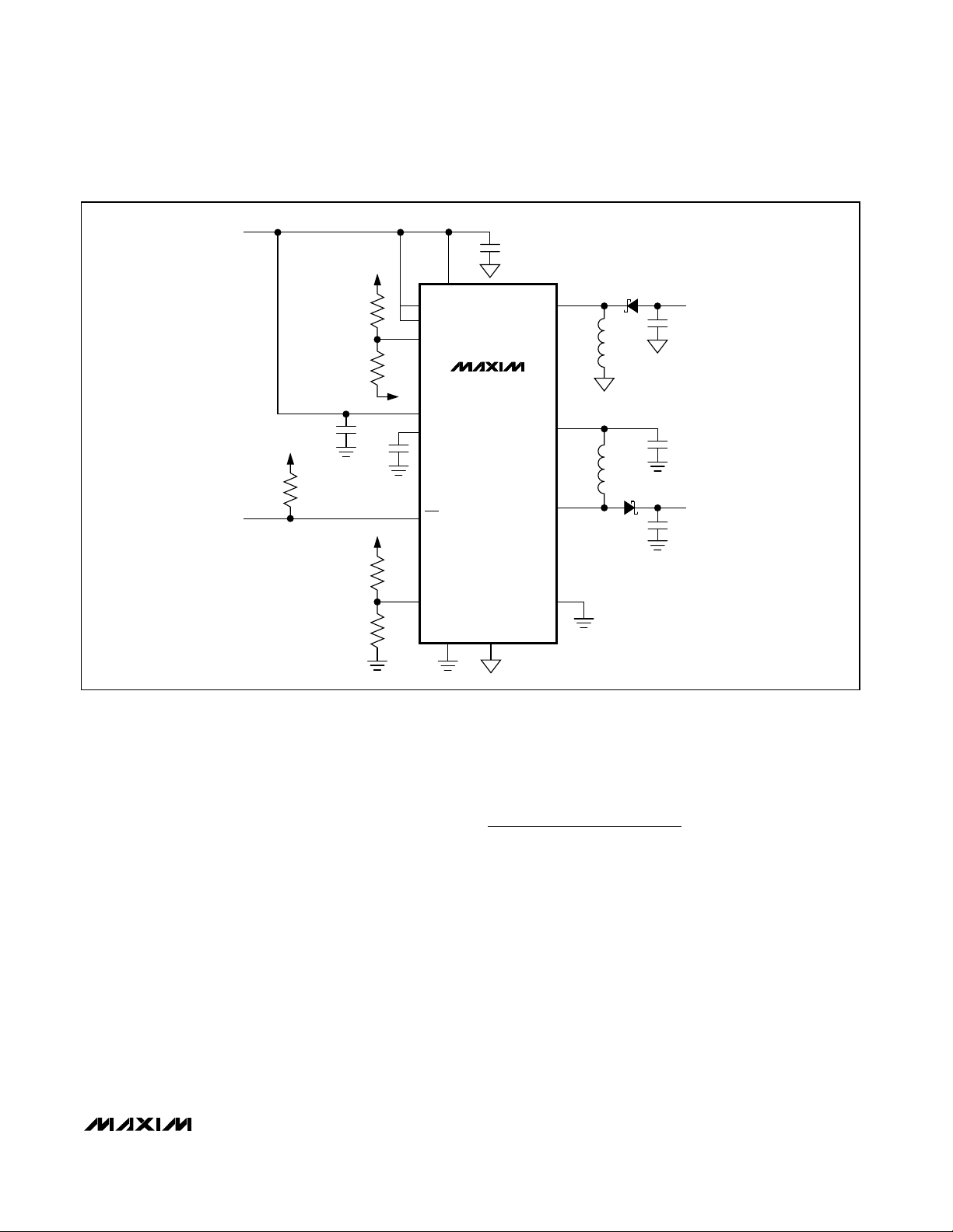
Figure 1. Typical Application Circuit
V
BATT
(2.7V ~ 5V)
FAULT
100kΩ
C4
MAX8614A
MAX8614B
4.7µF
LXN
PVP
LXP
SEQ
D2
4.7µH
2.2µH
L2
L1
CMHSH5-21
D1
CMHSH5-21
V
INV
-7.5V AT 100mA
C2
4.7µF
C3
1µF
V
BST
+15V AT 50mA
C1
2.2µF
14
12
10
8
V
INV
R3
187kΩ
1%
R4
30.9kΩ
1%
C5
0.1µF
V
BATT
R5
1.4MΩ
1%
100kΩ
1%
0.22µF
V
R1
R2
C6
BST
REF
1
9
2
3
4
6
7
ONBST
ONINV
FBN
AV
REF
FLT
13
V
CC
CC
FBP
GND PGND
511
Page 14

MAX8614A/MAX8614B
Dual-Output (+ and -) DC-DC
Converters for CCD
14 ______________________________________________________________________________________
MAX8614A/MAX8614B
Package Information
(The package drawing(s) in this data sheet may not reflect the most current specifications. For the latest package outline information,
go to www.maxim-ic.com/packages
.)
D
PIN 1
INDEX
AREA
E
A1
A
A2
DETAIL A
D2
PIN 1 ID
N
0.35x0.35
b
[(N/2)-1] x e
E2
k
C
L
L
e
e
REF.
e
C
L
L
6, 8, &10L, DFN THIN.EPS
PACKAGE OUTLINE, 6,8,10 & 14L,
TDFN, EXPOSED PAD, 3x3x0.80 mm
-DRAWING NOT TO SCALE-
21-0137
1
G
2
Page 15

MAX8614A/MAX8614B
Dual-Output (+ and -) DC-DC
Converters for CCD
Maxim cannot assume responsibility for use of any circuitry other than circuitry entirely embodied in a Maxim product. No circuit patent licenses are
implied. Maxim reserves the right to change the circuitry and specifications without notice at any time.
Maxim Integrated Products, 120 San Gabriel Drive, Sunnyvale, CA 94086 408-737-7600 ____________________ 15
© 2006 Maxim Integrated Products Printed USA is a registered trademark of Maxim Integrated Products, Inc.
MAX8614A/MAX8614B
Package Information (continued)
(The package drawing(s) in this data sheet may not reflect the most current specifications. For the latest package outline information,
go to www.maxim-ic.com/packages
.)
COMMON DIMENSIONS
SYMBOL
A
D
E 2.90 3.10
A1
L 0.20 0.40
A2 0.20 REF.
MIN. MAX.
0.70 0.80
2.90 3.10
0.00 0.05
0.25 MIN.k
PACKAGE VARIATIONS
PKG. CODE
T633-2 6 1.50±0.10 2.30±0.10 0.95 BSC
T833-2 8 1.50±0.10 2.30±0.10
T833-3 8 1.50±0.10 2.30±0.10
-DRAWING NOT TO SCALE-
N
D2 E2 e
2.30±0.101.50±0.106T633-1 0.95 BSC MO229 / WEEA 1.90 REF0.40±0.05
1.50±0.10
1.50±0.10
1.70±0.10 2.30±0.1014T1433-1
2.30±0.108T833-1
2.30±0.1010T1033-1
JEDEC SPEC
MO229 / WEEA
0.65 BSC
0.65 BSC MO229 / WEEC
0.65 BSC MO229 / WEEC
0.50 BSC
0.40 BSC
0.40 BSC
MO229 / WEEC
MO229 / WEED-3
- - - - 0.20±0.05 2.40 REFT1433-2 14 2.30±0.101.70±0.10
b
[(N/2)-1] x e
0.40±0.05 1.90 REF
1.95 REF0.30±0.05
0.30±0.05 1.95 REF
0.30±0.05 1.95 REF
2.00 REF0.25±0.05
2.40 REF0.20±0.05- - - -
DOWNBONDS
ALLOWED
NO
NO
NO
NO
YES
NO
YES
NO
PACKAGE OUTLINE, 6,8,10 & 14L,
TDFN, EXPOSED PAD, 3x3x0.80 mm
21-0137
2
G
2
 Loading...