

Page 1
General Description
The MAX8595Z/MAX8596Z drive up to 8 white LEDs
with constant current and high efficiency to provide
LCD backlighting in cell phones, PDAs, and other
handheld devices. The series connection allows the
LED currents to be identical for uniform brightness and
minimizes the number of traces to the LEDs. The
MAX8595Z regulates constant LED current over the
entire temperature range. The MAX8596Z features an
ambient-temperature derating function to avoid overdriving the white LEDs during high ambient temperatures, enabling higher drive current below +42°C.
A single Dual Mode™ input provides a simple means of
brightness adjustment and on/off control. Fast 1MHz
current-mode PWM operation allows for small input and
output capacitors and a small inductor while minimizing
ripple on the input supply/battery. Soft-start eliminates
inrush current during startup.
The MAX8595Z/MAX8596Z are available in a spacesaving, 8-pin 3mm x 3mm TDFN package.
Applications
Cell Phones and Smart Phones
PDAs, Palmtops, and Wireless Handhelds
e-Books and Subnotebooks
White LED Display Backlighting
Features
♦ Up to 8 LEDs at 25mA
♦ Temperature Derating Function to Allow Fewer
LEDs for Same Light (MAX8596Z)
♦ 86% Efficiency (P
LEDs
/ PIN)
♦ 1.7% Current-Regulation Accuracy
♦ Output Overvoltage Protection
♦ Flexible Dimming Control
Analog
Direct-PWM Internal Filter
♦ 1MHz PWM Switching Frequency
♦ 0.1µF Output Capacitor
♦ 12mV
P-P
Low Input Ripple
♦ Soft-Start Eliminates Inrush Current
♦ 2.6V to 5.5V Input Range
♦ 0.3µA Shutdown Current
♦ Pin Compatible with the MAX1561 and MAX1599
♦ TDFN 3mm x 3mm x 0.8mm Package with
Exposed Paddle
MAX8595Z/MAX8596Z
High-Efficiency, 32V Step-Up Converters
with TADerating Option for 2 to 8 White LEDs
________________________________________________________________ Maxim Integrated Products 1
GND
COMP
CS
1
2
LX
PGND
IN
CTRL
OUT
TOP VIEW
3
4
MAX8595Z
MAX8596Z
8
76
5
TDFN
3mm x 3mm x 0.8mm
Pin Configuration
Ordering Information
MAX8595Z
MAX8596Z
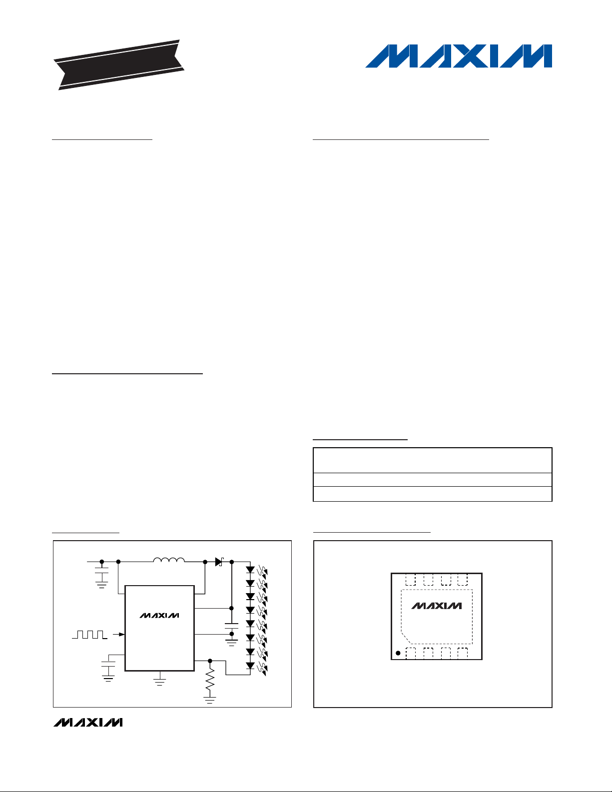
IN LX
OUT
PGND
CS
CTRL
COMP
GND
0.1µF
2 TO 8 LEDs
200Hz TO 200kHz
ANALOG OR
PWM DIMMING
2.2µF
INPUT
2.6V TO 5.5V
OUTPUT
UP TO 34V
Typical Operating Circuit
19-3558; Rev 0; 8/04
For pricing, delivery, and ordering information, please contact Maxim/Dallas Direct! at
1-888-629-4642, or visit Maxim’s website at www.maxim-ic.com.
EVALUATION KIT
AVAILABLE
PART
TEMP
RANGE
PIN-PACKAGE
PKG
CODE
MAX8595ZETA
T833-1
MAX8596ZETA
T833-1
Dual Mode is a trademark of Maxim Integrated Products, Inc.
-40°C to +85°C
-40°C to +85°C
8 TDFN 3mm x 3mm
8 TDFN 3mm x 3mm
Page 2
MAX8595Z/MAX8596Z
High-Efficiency, 32V Step-Up Converters
with T
A
Derating Option for 2 to 8 White LEDs
2 _______________________________________________________________________________________
ABSOLUTE MAXIMUM RATINGS
Stresses beyond those listed under “Absolute Maximum Ratings” may cause permanent damage to the device. These are stress ratings only, and functional
operation of the device at these or any other conditions beyond those indicated in the operational sections of the specifications is not implied. Exposure to
absolute maximum rating conditions for extended periods may affect device reliability.
IN to GND.................................................................-0.3V to +6V
PGND to GND .......................................................-0.3V to +0.3V
LX, OUT to GND.....................................................-0.3V to +37V
CTRL to GND...................-0.3V to the lower of +6V or (V
IN
+ 2V)
COMP, CS to GND ......................................-0.3V to (V
IN
+ 0.3V)
I
LX
...................................................................................1.0A
RMS
Continuous Power Dissipation (TA= +70°C)
8-Pin TDFN 3mm x 3mm
(derate 24.4mW/°C above +70°C)............................ 1950mW
Operating Temperature Range ...........................-40°C to +85°C
Junction Temperature......................................................+150°C
Storage Temperature Range.............................-65°C to +150°C
Lead Temperature (soldering, 10s).................................+300°C
ELECTRICAL CHARACTERISTICS
(VIN= 3.0V, L = 22µH, CIN= 2.2µF, C
OUT
= 0.1µF, C
COMP
= 0.1µF, R
SENSE
= 13Ω, V
CTRL
= 1.5V, TA= -40°C to +85°C, unless other-
wise noted. Typical values are at T
A
= +25°C.) (Note 1)
PARAMETER CONDITIONS
UNITS
Supply Voltage 2.6 5.5 V
UVLO Threshold V
IN
rising or falling
V
UVLO Hysteresis 30 mV
Quiescent Current No switching 0.5 0.7 mA
TA = +25°C 0.3 2
Shutdown Supply Current
CTRL = GND,
V
OUT
= V
IN T
A
= +85°C1
µA
OVLO Threshold V
OUT
rising 32 34 36 V
OVLO Hysteresis 2V
V
OUT
= 32V, V
CTRL
> 0.24V 9 20 35
TA = +25°C
1
OUT Input Bias Current
TA = +85°C 0.1
µA
Output Voltage Range (Note 2)
V
IN
-
V
D
32 V
ERROR AMPLIFIER
TA = +25°C
TA = 0°C to +85°C
CTRL to CS Regulation
V
CTRL
= 1.50V,
V
IN
= 2.6V to 5.5V
T
A
= -40°C to +85°C
V
TA = +25°C
1
CS Input Bias Current VCS = V
CTRL
/ 5
T
A
= +85°C
µA
MAX8595Z, V
CTRL
= 3.0V
347
TA = -40°C to +25°C
360
TA = +42°C
CS Maximum Brightness Clamp
Voltage
MAX8596Z,
V
CTRL
= 3.0V
T
A
= +85°C
mV
MAX8595Z
CTRL Voltage for CS Maximum
Brightness Clamp
MAX8596Z
V
CS Derating Function Start
Temperature
MAX8596Z, V
CTRL
= 3.0V
°C
MIN TYP MAX
2.10 2.38 2.55
OUT = IN, CTRL = GND
0.295 0.300 0.305
0.292 0.300 0.308
0.290 0.300 0.310
310 330
330 345
0.01
0.01
0.03
343
106.5
1.65
1.72
+42
Page 3
MAX8595Z/MAX8596Z
High-Efficiency, 32V Step-Up Converters
with T
A
Derating Option for 2 to 8 White LEDs
_______________________________________________________________________________________ 3
ELECTRICAL CHARACTERISTICS (continued)
(VIN= 3.0V, L = 22µH, CIN= 2.2µF, C
OUT
= 0.1µF, C
COMP
= 0.1µF, R
SENSE
= 13Ω, V
CTRL
= 1.5V, TA= -40°C to +85°C, unless other-
wise noted. Typical values are at T
A
= +25°C.) (Note 1)
PARAMETER CONDITIONS
MIN
TYP
MAX
UNITS
CS Derating Function Slope MAX8596Z, V
CTRL
= 3.0V, TA = +42°C to +85°C
mV/°C
CTRL Input Resistance V
CTRL
<
1.5V
780 kΩ
CTRL Dual-Mode Threshold
240 mV
CTRL Dual-Mode Hysteresis 5mV
CTRL Shutdown Enable Delay (Note 3) 6.0 8.2
ms
CS to COMP Transconductance
V
COMP
= 1.5V 32 50 82 µS
COMP Input Resistance to
Ground
In shutdown, UVLO or OVLO 20 kΩ
OSCILLATOR
Operating Frequency
1.0
MHz
PWM mode 12
Minimum Duty Cycle
Pulse skipping 0
%
Maximum Duty Cycle CTRL = IN, CS = GND 94 95 %
N-CHANNEL SWITCH
LX On-Resistance ILX = 190mA 0.8
Ω
TA = +25°C
5
LX Leakage Current
TA = +85°C1
µA
LX Current Limit Duty cycle = 90%
900 mA
Note 1: Parameters are 100% production tested at TA= +25°C. Limits over the operating temperature range are regulated by
design and characterization.
Note 2: V
D
is the forward-voltage drop of the Schottky diode in Figure 1.
Note 3: Time from CTRL going below the Dual-Mode threshold to IC shutdown.
VLX = 36V, CTRL = GND
-5.5
250 500
100 170
10.5
0.75
0.01
1.25
1.35
500 700
Page 4
MAX8595Z/MAX8596Z
High-Efficiency, 32V Step-Up Converters
with T
A
Derating Option for 2 to 8 White LEDs
4 _______________________________________________________________________________________
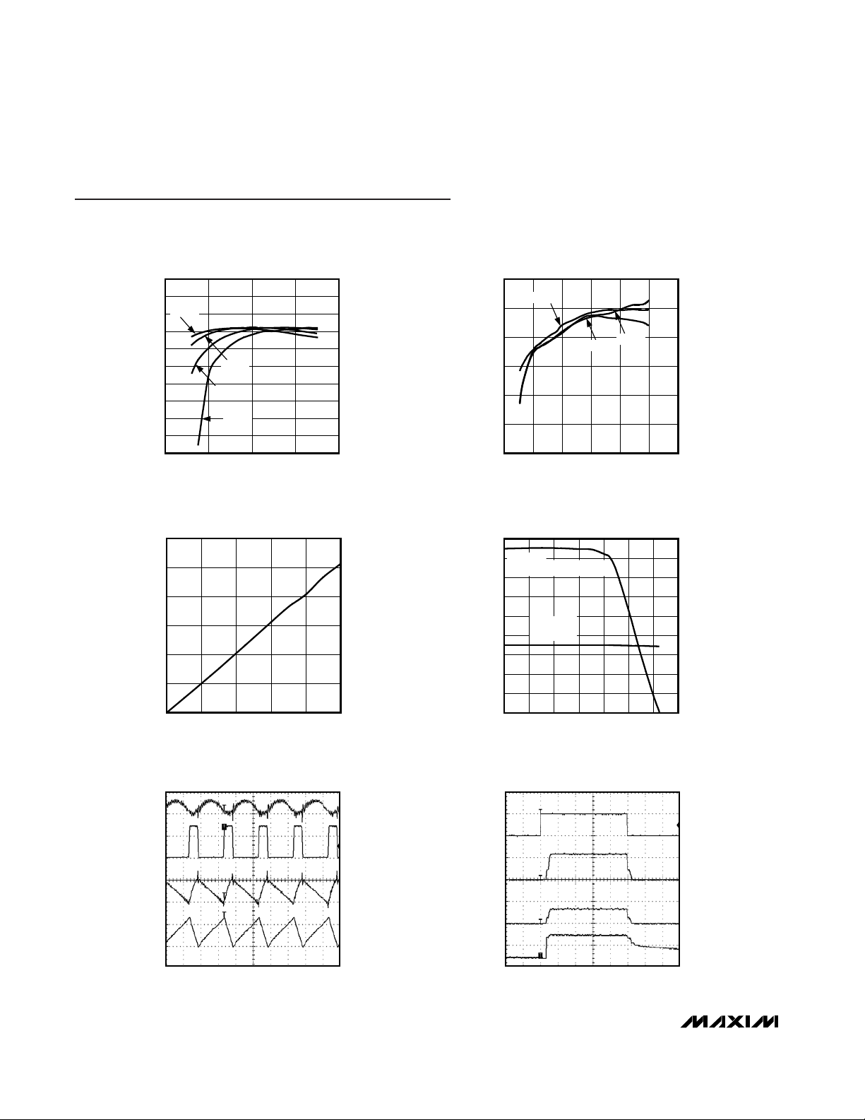
Typical Operating Characteristics
(Circuit of Figure 1, VIN= 3.6V, I
LED
= 25mA, L = 22µH, CIN= 2.2µF, C
OUT
= 0.1µF, C
COMP
= 0.1µF, R
SENSE
= 13Ω, 4 LEDs,
TA= +25°C, unless otherwise noted.)
EFFICIENCY
vs. INPUT VOLTAGE
MAX8595Z toc01
INPUT VOLTAGE (V)
EFFICIENCY (%)
543
55
60
65
70
75
80
85
90
95
100
50
26
3 LEDs
4 LEDs
6 LEDs
8 LEDs
EFFICIENCY
vs. LED CURRENT
MAX8595Z toc02
LED CURRENT (mA)
EFFICIENCY (%)
252015105
65
70
75
80
85
90
60
030
3 LEDs
6 LEDs
8 LEDs
LED CURRENT
vs. DIRECT-PWM DIMMING
MAX8595Z toc03
DUTY CYCLE (%)
LED CURRENT (mA)
80604020
5
10
15
20
25
30
0
0 100
LED CURRENT
vs. AMBIENT TEMPERATURE
MAX8595Z toc04
TEMPERATURE (°C)
LED CURRENT (mA)
806020 400-20
10
12
14
16
18
20
22
24
26
8
-40 100
MAX8596,
I
LED
= 25mA AT TA = +25°C
MAX8595,
I
LED
= 15mA
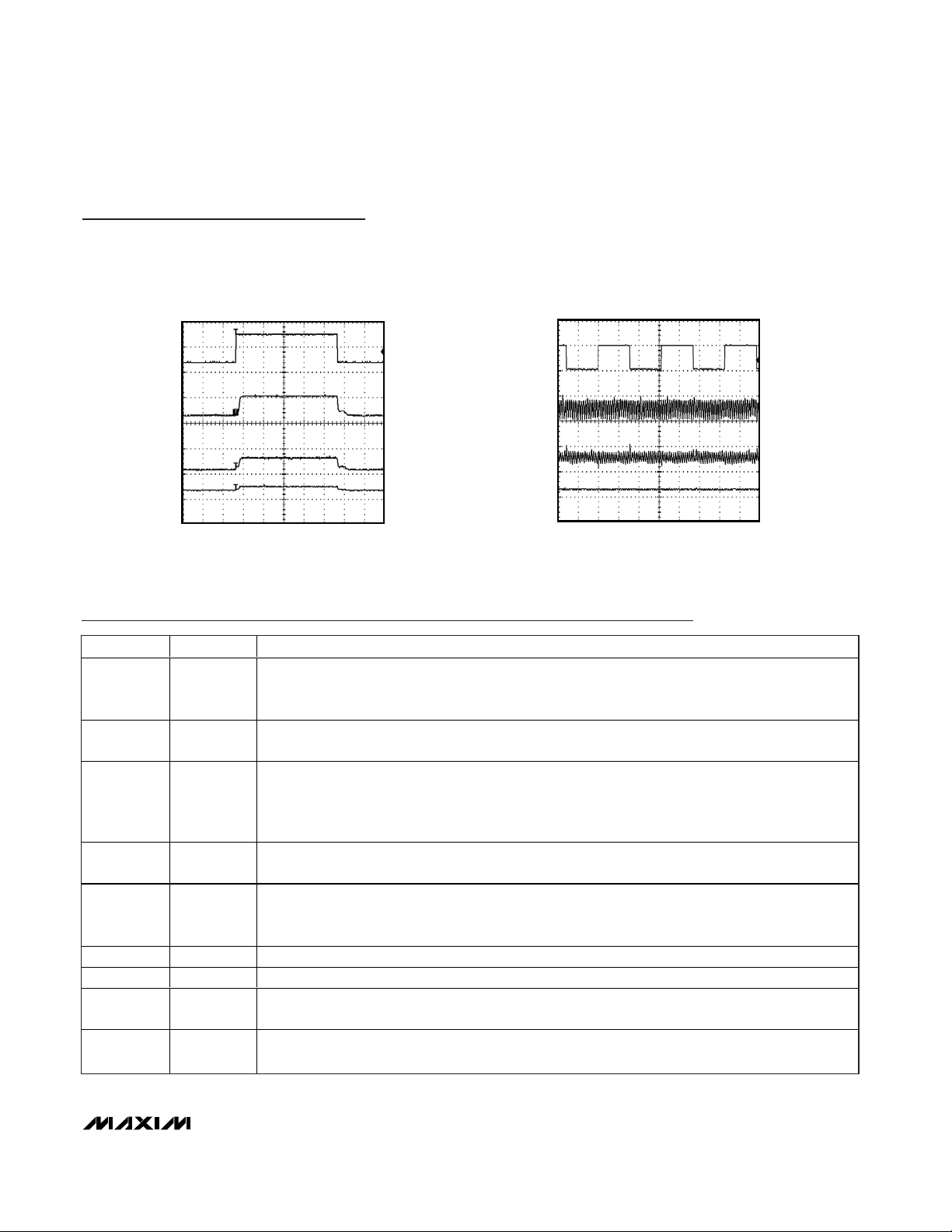
SWITCHING WAVEFORMS
MAX8595Z toc05
500ns/div
V
IN
20mV/div
AC-COUPLED
200mV/div
AC-COUPLED
100mA/div
10V/div
V
LX
V
OUT
I
L
SOFT-START AND SHUTDOWN RESPONSE
MAX8595Z toc06
20ms/div
V
CTRL
2V/div
0
0
0
0
40mA/div
10V/div
100mA/div
I
IN
I
LED
V
OUT
Page 5
MAX8595Z/MAX8596Z
High-Efficiency, 32V Step-Up Converters
with T
A
Derating Option for 2 to 8 White LEDs
_______________________________________________________________________________________ 5
Typical Operating Characteristics (continued)
(Circuit of Figure 1, VIN= 3.6V, I
LED
= 25mA, L = 22µH, CIN= 2.2µF, C
OUT
= 0.1µF, C
COMP
= 0.1µF, R
SENSE
= 13Ω, 4 LEDs,
TA= +25°C, unless otherwise noted.)
Pin Description
PIN NAME FUNCTION
1 OUT
Overvoltage Sense. When V
OUT
is greater than 34V (typ), the internal n-channel MOSFET turns off
until V
OUT
drops below 32V (typ), then the IC re-enters soft-start. Connect a 0.1µF ceramic capacitor
from OUT to ground. In shutdown, V
OUT
is one diode drop below VIN.
2IN
Input Voltage Supply. The input voltage range is 2.6V to 5.5V. Connect a 2.2µF ceramic capacitor
from IN to GND.
3 CTRL
Brightness Control Input. The voltage applied to CTRL controls LED brightness. Varying the voltage
from 0.24V to 1.65V (1.72V for the MAX8596Z) adjusts the brightness from dim to 100% brightness,
respectively. Any voltage above 1.65V (1.72V) does not increase brightness. Hold CTRL below
100mV to shut down the IC after an 8.2ms delay.
4CS
Current-Sense Feedback Input. Connect a resistor from CS to GND to set the LED bias current. The
voltage at CS regulates to V
CTRL
/ 5 or 0.330V (0.343V for the MAX8596Z), whichever is lower.
5 COMP
Compensation Input. Connect a 0.1µF ceramic capacitor (C
COMP
) from COMP to GND. C
COMP
stabilizes the converter, controls soft-start, and lowpass filters direct PWM dimming at CTRL. C
COMP
discharges to 0V through an internal 20kΩ resistor in shutdown.
6 GND Ground. Connect to PGND and the exposed pad directly under the IC.
7 PGND Power Ground. Connect to GND and the exposed pad directly under the IC.
8LX
Inductor Connection. Connect LX to the node between the inductor and the Schottky diode. LX is
high impedance in shutdown.
—EP
Exposed Pad. Connect to a large ground plane for maximum package heat dissipation. Connect
directly to GND and PGND under the IC.
CTRL STEP RESPONSE
V
CTRL
I
IN
I
LED
V
OUT
20ms/div
MAX8595Z toc07
1V/div
0
100mA/div
0
40mA/div
0
10V/div
0
V
CTRL
V
IN
V
OUT
I
LED
DIRECT-PWM DIMMING RESPONSE
10µs/div
MAX8595Z toc08
2V/div
32kHz 50%
DUTY CYCLE
0
20mV/div
AC-COUPLED
0
500mV/div
AC-COUPLED
0
10mA/div
0
Page 6
MAX8595Z/MAX8596Z
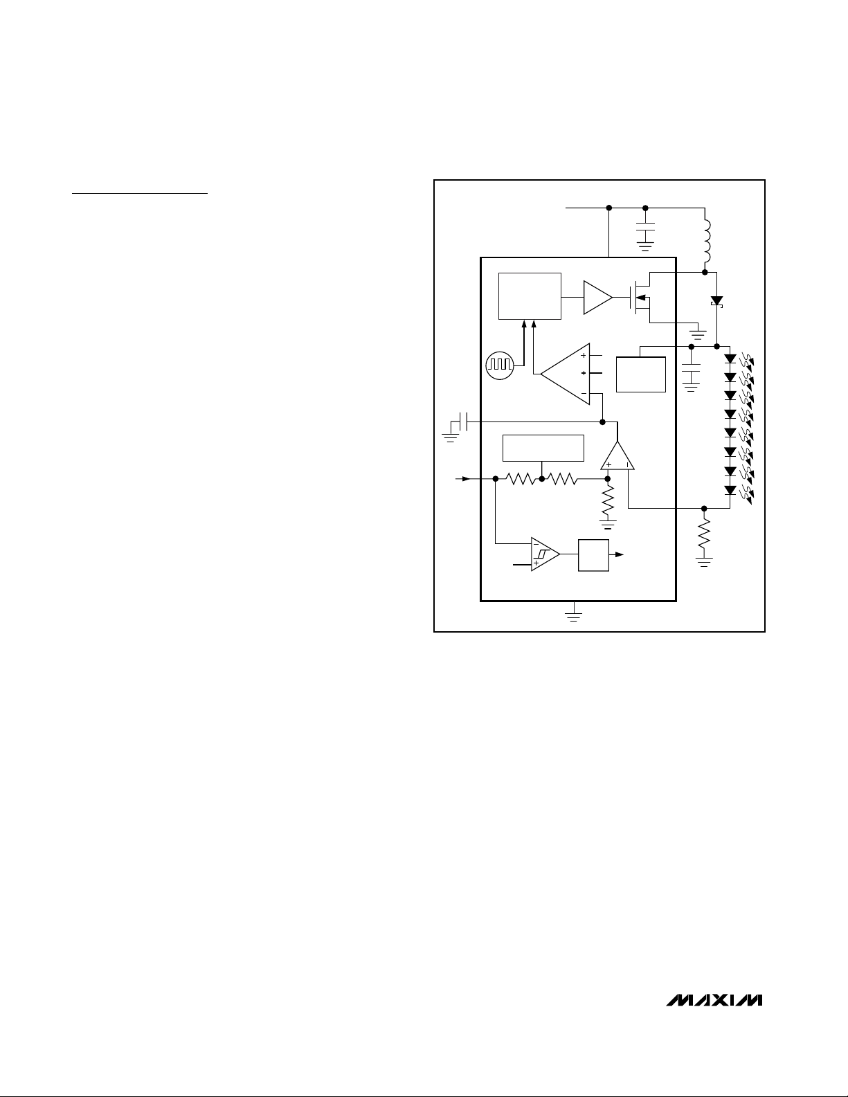
Detailed Description
The high efficiency and small size of the MAX8595Z/
MAX8596Z make them ideally suited to drive up to 8
series-connected LEDs. These devices operate as a
boost DC-DC converter that regulates output current
rather than voltage. The MAX8595Z/MAX8596Z provide
even illumination by sourcing the same output current
through each LED, eliminating the need for expensive
factory calibration. The fast 1MHz internal oscillator
allows for a small inductor and small input and output
capacitors while minimizing input and output ripple.
The single analog control input (CTRL) allows easy
adjustment of LED brightness and on/off control. This
allows simple logic-level on/off control, analog voltage
control, or PWM duty-cycle control of both brightness
and shutdown. In shutdown, supply current is reduced
to a low 0.3µA (typ). A soft-start gradually illuminates
the LEDs, eliminating the inrush current during startup.
The MAX8596Z has the additional feature of derating
LED current as ambient temperature rises. Above
+42°C, the CS regulation voltage is reduced at a rate of
5.5mV/°C, thus reducing the LED current.
Soft-Start
The MAX8595Z/MAX8596Z attain soft-start by charging
C
COMP
gradually with a current source. When V
COMP
rises above 1.25V, the internal MOSFET begins switching at a reduced duty cycle. When V
COMP
rises above
2.25V, the duty cycle is at its maximum. See the
Typical Operating Characteristics for an example of
soft-start operation.
Shutdown
The MAX8595Z/MAX8596Z enter shutdown when V
CTRL
is less than 100mV for more than 8.2ms. In shutdown,
supply current is reduced to 0.3µA (typ) by powering
down the entire IC except for the CTRL voltage-detection circuitry. C
COMP
is discharged during shutdown,
allowing the device to re-initiate soft-start when it is
enabled. Although the internal n-channel MOSFET does
not switch in shutdown, there is still a DC current path
between the input and the LEDs through the inductor
and Schottky diode. The minimum forward voltage of the
LED array must exceed the maximum input voltage to
ensure that the LEDs remain off in shutdown. However,
with 2 or more LEDs, the forward voltage is large
enough to keep leakage current low, less than 1µA
(typ). Typical shutdown timing characteristics are shown
in the Typical Operating Characteristics.
Overvoltage Protection
Overvoltage lockout (OVLO) occurs when V
OUT
is
above 34V (typ). The protection circuitry stops the inter-
nal MOSFET from switching and causes V
COMP
to
decay towards 0V. The device comes out of OVLO and
into soft-start when V
OUT
falls below 32V (typ).
Ambient Temperature Derating Function
(MAX8596Z)
The MAX8596Z limits the maximum LED current
depending on the die temperature. VCSis limited to
343mV up to +42°C. Once the temperature reaches
+42°C, the maximum V
CS
declines by 5.5mV/°C until
the minimum 106.5mV threshold is reached at +85°C.
Due to the package’s exposed paddle, the die temperature is always very close to the PC board temperature.
The temperature derating function allows the LED current to be safely set higher at normal operating temperatures, thereby allowing either a brighter display or
fewer LEDs to be used for normal display brightness.
See the Typical Operating Characteristics for LED
Current vs. Ambient Temperature.
High-Efficiency, 32V Step-Up Converters
with T
A
Derating Option for 2 to 8 White LEDs
6 _______________________________________________________________________________________
0.1µF
PWM
CONTROL
IN
2.2µF
22µH
LX
PGND
OVERVOLTAGE
PROTECT
g
m
CS
SHUTDOWN8.2ms
GND
COMP
CTRL
170mV
100kΩ
121kΩ
279kΩ
1.25V CLAMP OR
TEMP DERATE CLAMP
R
SENSE
13Ω
2.6V TO 5.5V
f
OSC
1MHz
0.1µF
ANALOG
OR DIRECT
PWM
DIMMING
OUT
Figure 1. Functional Diagram and Typical Application Circuit
Page 7

Design Procedure
Adjusting LED Current
Adjusting the output current of the MAX8595Z/
MAX8596Z changes the brightness of the LEDs. An
analog input (CTRL) and the sense-resistor value set
the output current. Output current is given by:
I
LED
= V
CTRL
/ (5 x R
SENSE
)
The V
CTRL
voltage range for adjusting output current is
0.24V to 1.65V (or 1.72V for the MAX8596Z). To set the
maximum current, calculate R
SENSE
when V
CTRL
is at
its maximum as follows:
For the MAX8595Z, R
SENSE
= 1.65 / (5 x I
LED(MAX)
)
For the MAX8596Z, R
SENSE
= 1.72 / (5 x I
LED(MAX)
)
Power dissipation in R
SENSE
is typically less than 10mW,
allowing the use of a small surface-mount resistor.
PWM Dimming Control
CTRL is also used as a digital input allowing LED
brightness control with a logic-level PWM signal
applied directly to CTRL. The frequency range is from
200Hz to 200kHz, while 0% duty cycle corresponds to
zero current and 100% duty cycle corresponds to full
current. The error amplifier and compensation capacitor form a lowpass filter so PWM dimming results in DC
current to the LEDs without the need for any additional
RC filters; see the Typical Operating Characteristics.
Capacitor Selection
Ceramic capacitors with X5R, X7R, or better dielectric
are recommended for stable operation over the entire
operating temperature range. The exact values of input
and output capacitors are not critical. The typical value
for the input capacitor is 2.2µF, and the typical value for
the output capacitor is 0.1µF. Higher-value capacitors
can be used to reduce input and output ripple, but at
the expense of size and higher cost. C
COMP
stabilizes
the converter and controls soft-start. Connect a 0.1µF
capacitor from COMP to GND. For stable operation,
C
OUT
must not exceed 10 times C
COMP
.
Inductor Selection
Inductor values range from 10µH to 47µH. A 22µH
inductor optimizes the efficiency for most applications
while maintaining low 12mV
P-P
input ripple. With input
voltages near 5V, a larger value of inductance can be
more efficient. To prevent core saturation, ensure that
the inductor-saturation current rating exceeds the peak
inductor current for the application. Calculate the peak
inductor current with the following formula:
Schottky Diode Selection
The high switching frequency of the MAX8595Z/
MAX8596Z demands a high-speed rectification diode
(D1) for optimum efficiency. A Schottky diode is recommended due to its fast recovery time and low forwardvoltage drop. Ensure that the diode’s average and
peak current rating exceed the average output current
and peak inductor current. In addition, the diode’s
reverse breakdown voltage must exceed V
OUT
. The
RMS diode current can be approximated from:
Applications Information
PC Board Layout
Due to fast switching waveforms and high-current
paths, careful PC board layout is required. An evaluation kit (MAX8596ZEVKIT) is available to speed design.
When laying out a board, minimize trace lengths
between the IC and R
SENSE
, the inductor, the diode,
the input capacitor, and the output capacitor. Keep
traces short, direct, and wide. Keep noisy traces, such
as the LX node trace, away from CS. The IN bypass
capacitor (CIN) should be placed as close to the IC as
possible. PGND and GND should be connected directly to the exposed paddle underneath the IC. The
ground connections of CINand C
OUT
should be as
close together as possible. The traces from IN to the
inductor and from the Schottky diode to the LEDs can
be longer.
Chip Information
TRANSISTOR COUNT: 2143
PROCESS: BiCMOS
III
DIODE RMS OUT PEAK()
=×
I
VIVVs
L
PEAK
OUT MAX LED MAX
IN MIN
IN MIN
=
×
×
+
×
×
() ()
()
()
..09
09
2
µ
MAX8595Z/MAX8596Z
High-Efficiency, 32V Step-Up Converters
with T
A
Derating Option for 2 to 8 White LEDs
_______________________________________________________________________________________ 7
Page 8
MAX8595Z/MAX8596Z
High-Efficiency, 32V Step-Up Converters
with T
A
Derating Option for 2 to 8 White LEDs
Maxim cannot assume responsibility for use of any circuitry other than circuitry entirely embodied in a Maxim product. No circuit patent licenses are
implied. Maxim reserves the right to change the circuitry and specifications without notice at any time.
8 _____________________Maxim Integrated Products, 120 San Gabriel Drive, Sunnyvale, CA 94086 408-737-7600
© 2004 Maxim Integrated Products Printed USA is a registered trademark of Maxim Integrated Products.
Package Information
(The package drawing(s) in this data sheet may not reflect the most current specifications. For the latest package outline information,
go to www.maxim-ic.com/packages
.)
PIN 1
INDEX
AREA
D
N
E
A
DETAIL A
L
E2
C
L
e
C
L
L
e
6, 8, &10L, DFN THIN.EPS
PACKAGE OUTLINE, 6, 8, 10 & 14L,
NUMBER OF LEADS SHOWN ARE FOR REFERENCE ONLY
TDFN, EXPOSED PAD, 3x3x0.80 mm
21-0137
1
F
2
COMMON DIMENSIONS
MIN. MAX.
SYMBOL
A 0.70 0.80
D 2.90 3.10
E 2.90 3.10
A1 0.00 0.05
L
A2 0.20 REF.
PACKAGE VARIATIONS
PKG. CODE
T833-1
T1033-1
0.40
0.20
0.25 MIN.k
N D2 E2 e
2.30±0.101.50±0.106T633-1 0.95 BSC MO229 / WEEA
1.50±0.10
2.30±0.108
1.50±0.10
1.70±0.10 2.30±0.1014T1433-1
1.70±0.10
0.65 BSC
2.30±0.1010
0.50 BSC
0.40 BSC
0.40 BSC
JEDEC SPEC
MO229 / WEEC
MO229 / WEED-3
- - - - 0.20±0.03 2.40 REFT1433-2 14 2.30±0.10
b
0.40±0.05
[(N/2)-1] x e
1.90 REF
1.95 REF0.30±0.05
2.00 REF0.25±0.05
2.40 REF0.20±0.03- - - -
PACKAGE OUTLINE, 6, 8, 10 & 14L,
TDFN, EXPOSED PAD, 3x3x0.80 mm
21-0137
2
F
2
 Loading...