

Page 1
General Description
The MAX8570 family of LCD step-up converters uses
an internal n-channel switch and an internal p-channel
output isolation switch. These converters operate from
a 2.7V to 5.5V supply voltage and deliver up to 28V at
the output.
A unique control scheme provides the highest efficiency over a wide range of load conditions. The internal
MOSFET switch reduces external component count and
a high switching frequency (up to 800kHz) allows for
tiny surface-mount components. Three current-limit
options are available. The MAX8570 and MAX8572 use
a 110mA current limit to reduce ripple and component
size in low-current applications. For high-power requirements, the MAX8574 and MAX8575 use a 500mA current limit and supply up to 20mA at 20V. The MAX8571
and MAX8573 use a 250mA current limit for a compromise between ripple and power. Built-in safety features
protect the internal switch and down-stream components from fault conditions.
Additional features include a low quiescent current and
a True Shutdown mode to save power. The MAX8570/
MAX8571/MAX8574 allow the user to set the output
voltage between 3V and 28V, and the MAX8572/
MAX8573/MAX8575 have a preset 15V output. These
step-up converters are ideal for small LCD panels with
low current requirements, but can also be used in other
applications. The MAX8571 evaluation kit is available to
help reduce design time.
Applications
LCD Bias Generators
Polymer LEDs (OLED)
Cellular or Cordless Phones
Palmtop Computers
Personal Digital Assistants (PDAs)
Organizers
Handy Terminals
Features
♦ 15V or Adjustable Output Voltage Up to 28V
♦ Safety Features Protect Against Output Faults
♦ 20mA at 20V from a Single Li+ Battery
♦ True Shutdown
♦ 87% Efficiency
♦ Up to 800kHz Switching Frequency
♦ Small 6-Pin SOT23 Package
MAX8570–MAX8575
High-Efficiency LCD Boost
with True Shutdown
________________________________________________________________ Maxim Integrated Products 1
Ordering Information
19-3329; Rev 0; 7/04
For pricing, delivery, and ordering information, please contact Maxim/Dallas Direct! at
1-888-629-4642, or visit Maxim’s website at www.maxim-ic.com.
EVALUATION KIT
AVAILABLE
PART TEMP RANGE
PIN-
TOP
MARK
MAX8570EUT-T*
6 SOT23-6
ABTJ
MAX8571EUT-T*
6 SOT23-6
ABTK
MAX8572EUT-T
6 SOT23-6
ABTL
MAX8573EUT-T
6 SOT23-6
ABTM
MAX8574EUT-T*
6 SOT23-6
ABTN
MAX8575EUT-T
6 SOT23-6
ABTO
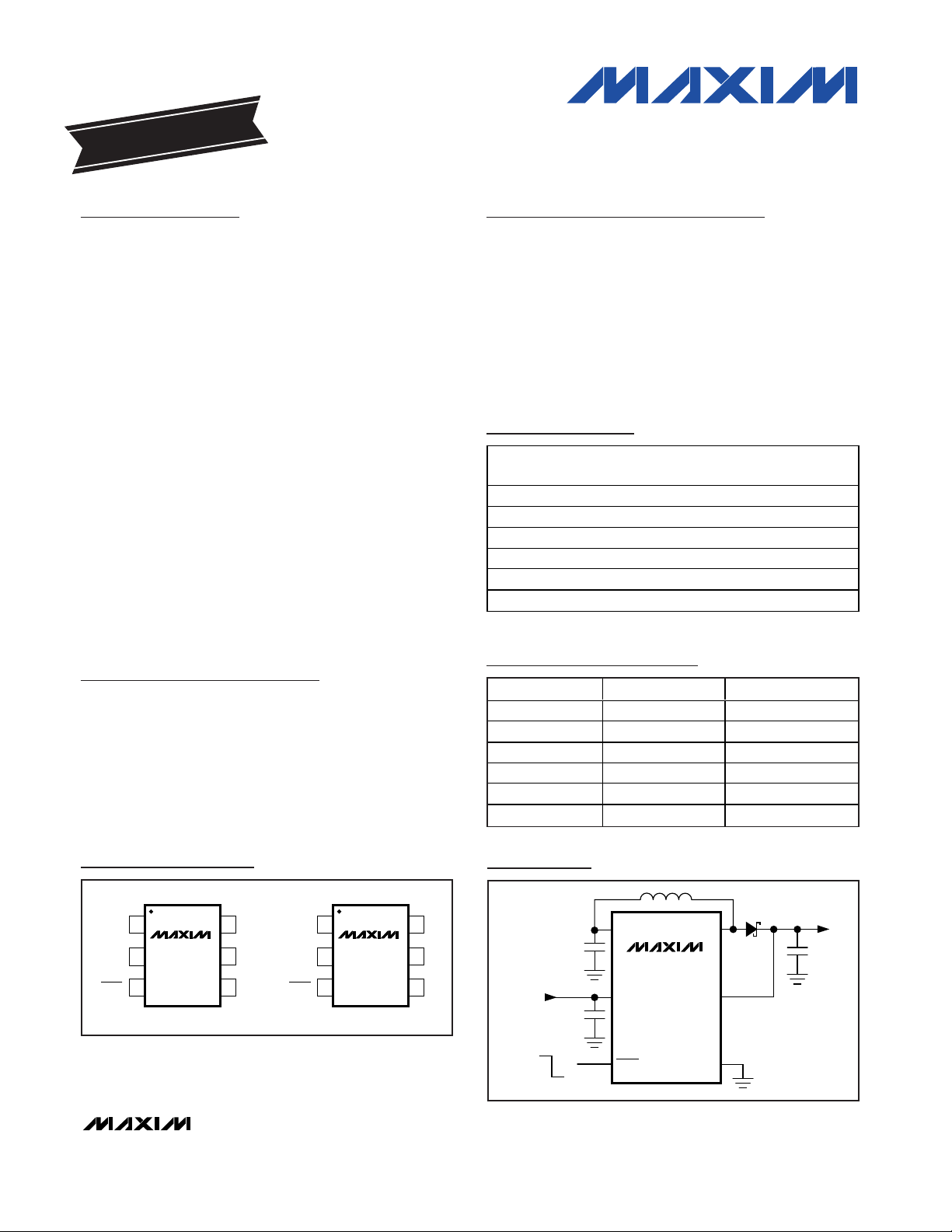
GND
LX
16V
CC
5SW
FB
MAX8570
MAX8571
MAX8574
SOT23-6
TOP VIEW
2
34SHDN
GND
LX
16V
CC
5SW
OUT
MAX8572
MAX8573
MAX8575
SOT23-6
2
34SHDN
Pin Configurations
PART
OUTPUT VOLTAGE
MAX8570EUT 110mA Adjustable
MAX8571EUT 250mA Adjustable
MAX8572EUT 110mA 15V
MAX8573EUT 250mA 15V
MAX8574EUT 500mA Adjustable
MAX8575EUT 500mA 15V
Selector Guide
True Shutdown is a trademark of Maxim Integrated Products,
Inc.
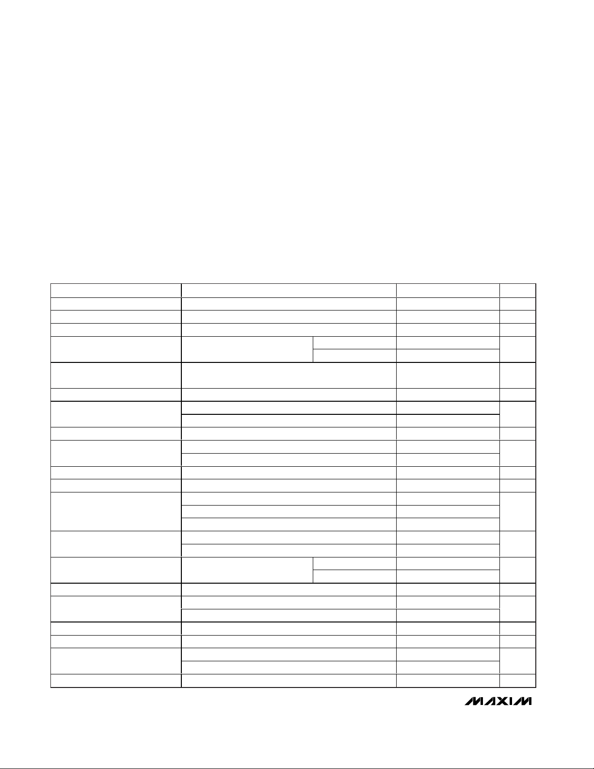
MAX8572
MAX8573
MAX8575
SW
V
CC
LX
OUT
GND
ON
OFF
V
CC
= 2.7V TO 5.5V
V
OUT
= VCC TO 28V
SHDN
Typical Operating Circuit
*Future products—contact factory for availability.
PACKAGE
-40°C to +85°C
-40°C to +85°C
-40°C to +85°C
-40°C to +85°C
-40°C to +85°C
-40°C to +85°C
CURRENT LIMIT
Page 2
MAX8570–MAX8575
High-Efficiency LCD Boost
with True Shutdown
2 _______________________________________________________________________________________
ABSOLUTE MAXIMUM RATINGS
ELECTRICAL CHARACTERISTICS
(VCC= V
SHDN
= 3.6V, SW floating, VFB= 1.3V (MAX8570/MAX8571/MAX8574) or V
OUT
= 16V (MAX8572/MAX8573/MAX8575), TA=
-40°C to +85°C, unless otherwise noted. Typical values are at T
A
= +25°C.) (Note 1)
Stresses beyond those listed under “Absolute Maximum Ratings” may cause permanent damage to the device. These are stress ratings only, and functional
operation of the device at these or any other conditions beyond those indicated in the operational sections of the specifications is not implied. Exposure to
absolute maximum rating conditions for extended periods may affect device reliability.
VCC, SHDN to GND..................................................-0.3V to +6V
SW to GND .................................................-0.3V to (V
CC
+ 0.3V)
FB to GND (MAX8570/MAX8571/
MAX8574)...............................................-0.3V to (V
CC
+ 0.3V)
OUT to GND (MAX8572/MAX8573/MAX8575) .......-0.3V to +30V
LX to GND ..............................................................-0.3V to +30V
I
LX
, ICC..............................................................................600mA
Continuous Power Dissipation (T
A
= +70°C)
SOT23-6 (derate 8.7 mW/°C above +70°C).............695.7 mW
Operating Temperature Range ...........................-40°C to +85°C
Junction Temperature......................................................+150°C
Storage Temperature Range .............................-65°C to +150°C
Lead Temperature (soldering, 10s) .................................+300°C
PARAMETER CONDITIONS
UNITS
VCC Input Voltage Range
V
VCC Undervoltage Lockout VCC rising, 50mV typical hysteresis
2.5
V
VCC Supply Current 25 35 µA
TA = +25°C
1
VCC Shutdown Current SHDN = GND, VCC = 5.5V
µA
Line Regulation
Circuit of Figure 3, V
OUT
= 15V, I
LOAD
= 5mA,
V
CC
= 2.7V to 5.5V
0.1 %/V
Load Regulation Circuit of Figure 3, V
OUT
= 15V, I
LOAD
= 0 to 5mA 0.1
%/mA
TA = 0°C to +85°C
FB Regulation Voltage
T
A
= -40°C to +85°C
V
FB Input Bias Current -50 -4
nA
TA = 0°C to +85°C
15
OUT Regulation Voltage
T
A
= -40°C to +85°C
V
OUT Input Bias Current V
OUT
= 15V 2.4 4.4 µA
LX Voltage Range 28 V
MAX8571/MAX8573
MAX8570/MAX8572
LX Switch Current Limit (Note 2)
MAX8574/MAX8575
A
MAX8571/MAX8573/MAX8574/MAX8575, I
LX
= 100mA 0.9 1.5
LX On-Resistance
MAX8570/MAX8572, I
LX
= 50mA 1.5 2.4
Ω
TA = +25°C
2
LX Leakage Current V
LX
= 28V
µA
Maximum LX On-Time 81114µs
VFB > 1V or V
OUT
> 12.2V 0.8 1 1.2
Minimum LX Off-Time
V
FB
= 0.25V or V
OUT
= 3.4V 4.0 5 6.0
µs
Current-Limit Propagation Delay
55 ns
SHDN Low Level (VIL)2.7V ≤ VCC ≤ 5.5V 0.7 V
4.2V ≤ VCC ≤ 5.5V 1.5
SHDN High Level (VIH)
2.7V ≤ V
CC
< 4.2V 1.4
V
SHDN Leakage Current -1 +1 µA
MIN TYP MAX
2.70 5.50
2.33
2.65
TA = -40°C to +85°C 0.05
TA = -40°C to +85°C 0.05
1.216 1.226 1.236
1.2137 1.2383
14.85
14.813 15.187
0.217 0.241 0.267
0.088 0.101 0.108
0.425 0.484 0.540
0.05
0.01
+50
15.15
Page 3
MAX8570–MAX8575
High-Efficiency LCD Boost
with True Shutdown
_______________________________________________________________________________________ 3
EFFICIENCY vs. SUPPLY VOLTAGE
MAX8570/71/73/74/75 toc06
SUPPLY VOLTAGE (V)
EFFICIENCY (%)
5.14.74.33.93.53.1
75
80
85
90
95
100
70
2.7 5.5
L1 = TOKO A914BYW-470M
47µH, 1mA LOAD
47µH, 5mA LOAD
L1 = MURATA LQH32CN220K23
22µH, 5mA LOAD
22µH, 1mA LOAD
Typical Operating Characteristics
(MAX8571, VCC= 3.6V, V
OUT
= 18V, Circuit of Figure 2, TA= +25°C, unless otherwise noted.)
OUTPUT VOLTAGE
vs. SUPPLY VOLTAGE (MAX8571)
MAX8570/71/73/74/75 toc01
SUPPLY VOLTAGE (V)
OUTPUT VOLTAGE (V)
5.14.73.9 4.33.53.1
17.6
17.7
17.8
17.9
18.0
18.1
18.2
18.3
18.4
18.5
17.5
2.7 5.5
L1 = MURATA LQH32CN220K23
R1 = 3.9MΩ, R2 = 287kΩ
5mA LOAD
1mA LOAD
OUTPUT VOLTAGE
vs. SUPPLY VOLTAGE (FIGURE 3, MAX8573)
MAX8570/71/73/74/75 toc02
SUPPLY VOLTAGE (V)
OUTPUT VOLTAGE (V)
5.14.73.9 4.33.53.1
14.6
14.7
14.8
14.9
15.0
15.1
15.2
15.3
15.4
15.5
14.5
2.7 5.5
L1 = MURATA LQH32CN220K23
5mA LOAD
1mA LOAD
OUTPUT VOLTAGE
vs. SUPPLY VOLTAGE (MAX8574)
MAX8570/71/73/74/75 toc03
SUPPLY VOLTAGE (V)
OUTPUT VOLTAGE (V)
4.64.34.03.73.4
17.2
18.2
18.0
17.8
17.6
17.4
18.4
18.6
18.8
19.0
17.0
3.1 4.9
L1 = TOKO S1024-100M
R1 = 1.1MΩ, R2 = 75kΩ, C4 = 4.7pF
5mA LOAD
20mA LOAD
OUTPUT VOLTAGE
vs. LOAD CURRENT
MAX8570/71/73/74/75 toc04
LOAD CURRENT (mA)
OUTPUT VOLTAGE (V)
20155 10
17.6
17.8
18.0
18.2
18.4
18.6
18.8
19.0
17.4
025
L1 = MURATA LQH32CN220K23
R1 = 3.9MΩ, R2 = 287kΩ, C4 = 10pF
MAX8570 MAX8571
MAX8574, R1 = 1.1MΩ, R2 = 75kΩ, C4 = 4.7pF
OUTPUT VOLTAGE vs. TEMPERATURE
MAX8570/71/73/74/75 toc05
TEMPERATURE (°C)
OUTPUT VOLTAGE (V)
603510-15
17.7
17.8
17.9
18.0
18.1
18.2
18.3
18.4
17.6
-40 85
1mA LOAD
Note 1: Parameters are production tested at TA= +25°C. Limits over temperature are guaranteed by design.
Note 2: Specified currents are measured at DC. Actual LX current limits are slightly higher in circuit due to current-limit comparator
delay. Actual currents (with 2µH) are 110mA (MAX8570/MAX8572), 250mA (MAX8571/MAX8573), and 500mA
(MAX8574/MAX8575).
ELECTRICAL CHARACTERISTICS (continued)
(VCC= V
SHDN
= 3.6V, SW floating, VFB= 1.3V (MAX8570/MAX8571/MAX8574) or V
OUT
= 16V (MAX8572/MAX8573/MAX8575), TA=
-40°C to +85°C, unless otherwise noted. Typical values are at T
A
= +25°C.) (Note 1)
PARAMETER CONDITIONS
MIN
TYP
MAX
UNITS
VCC = 3.6V, VSW = 0V, VFB = 0V, ICC (peak)
SW PMOS Current Limit
V
CC
= 3.6V, VSW = 0V, VFB = 0V, ICC (average)
A
SW PMOS On-Resistance VCC = 2.7V, VFB = 0V, I
SW
= 100mA 1.5 2.5 Ω
TA = +25°C
1
SW PMOS Leakage Current
µA
SW Soft-Start Time VCC = 2.7V, CSW = 4.7µF 0.2 1 ms
0.45 0.75 1.10
0.15 0.30 0.60
SW = GND, VCC = 5.5V, VFB = 0V
= -40°C to +85°C 0.02
T
A
0.01
Page 4

MAX8570–MAX8575
High-Efficiency LCD Boost
with True Shutdown
4 _______________________________________________________________________________________
EFFICIENCY vs. BATTERY VOLTAGE
(FIGURE 4)
MAX8570/71/73/74/75 toc07
BATTERY VOLTAGE (V)
EFFICIENCY (%)
108642
50
60
70
80
90
100
40
012
L1 = MURATA LQH32CN220K23
5mA LOAD
1mA LOAD
VCC = 3.6V
EFFICIENCY vs. LOAD CURRENT
WITH 22µH INDUCTOR
MAX8570/71/73/74/75 toc08
LOAD CURRENT (mA)
EFFICIENCY (%)
101
50
60
70
80
90
100
40
0.1 100
MAX8574, TOKO A914BYW-220M
MAX8571, MURATA LQH32CN220K23
MAX8570, MURATA LQH32CN220K23
EFFICIENCY vs. LOAD CURRENT
WITH 47µH INDUCTOR
MAX8570/71/73/74/75 toc09
LOAD CURRENT (mA)
EFFICIENCY (%)
101
50
60
70
80
90
100
40
0.1 100
MAX8570, L1 = MURATA LQH32CN470K23
MAX8571, L1 = TOKO A914BYW-470M
PEAK INDUCTOR CURRENT LIMIT
vs. SUPPLY VOLTAGE
MAX8570/71/73/74/75 toc10
SUPPLY VOLTAGE (V)
CURRENT LIMIT (mA)
5.14.74.33.93.53.1
100
200
300
400
500
600
700
0
2.7 5.5
MAX8574
MAX8571
MAX8570
SUPPLY CURRENT vs. LOAD CURRENT
MAX8570/71/73/74/75 toc11
LOAD CURRENT (mA)
SUPPLY CURRENT (mA)
105
20
40
60
80
100
120
0
015
L1 = MURATA LQH32CN220K23
NO-LOAD CURRENT vs. SUPPLY VOLTAGE
MAX8570/71/73/74/75 toc12
SUPPLY VOLTAGE (V)
SUPPLY CURRENT (µA)
541 2 3
10
20
30
40
50
60
70
80
0
06
R1 = 3.9MΩ
R2 = 287kΩ
R1 = 7.87MΩ
R2 = 576kΩ
MAX8573,
FIGURE 3
L1 = MURATA
LQH32CN220K23
NO SWITCHING
LINE TRANSIENT 3V TO 5.5V (MAX8571)
MAX8570/71/73/74/75 toc13
100µs/div
V
CC
V
OUT
200mV/div
(AC-COUPLED)
2V/div
0
3.6kΩ LOAD, R1 = 3.9MΩ, R2 = 287kΩ
LINE TRANSIENT 3V TO 5.5V
(FIGURE 3, MAX8573)
MAX8570/71/73/74/75 toc14
100µs/div
V
CC
V
OUT
200mV/div
(AC-COUPLED)
2V/div
0
3kΩ LOAD
Typical Operating Characteristics (continued)
(MAX8571, VCC= 3.6V, V
OUT
= 18V, Circuit of Figure 2, TA= +25°C, unless otherwise noted.)
Page 5

MAX8570–MAX8575
High-Efficiency LCD Boost
with True Shutdown
_______________________________________________________________________________________ 5
PIN NAME FUNCTION
FB
(MAX8570/
Feedback for setting the output voltage. Connect FB to the center of a resistor voltage-divider from the
output to GND to set positive output voltages.
1
OUT
(MAX8572/
Output. The output voltage is preset to 15V. Connect a 1µF ceramic capacitor from OUT to GND. In
shutdown, OUT is pulled to GND by an internal 7.5MΩ resistor.
2 GND Ground
3 SHDN
Shutdown Input. A logic low at SHDN places the part in low-power shutdown mode. Pull SHDN high or
connect to V
CC
for normal operation.
4LXInductor Switching Connection
5SW
Isolation Switch Output. Internally connected to the drain of a p-channel MOSFET used to isolate the
output from the input during shutdown. Connect a 4.7µF ceramic capacitor from SW to GND. If true
shutdown is not required, SW can be left open with the input supply connected directly to the inductor.
6V
CC
Input Voltage Supply. Connect a 2.7V to 5.5V input supply to VCC. Connect a 1µF ceramic capacitor from
V
CC
to GND.
Pin Description
LOAD TRANSIENT
MAX8570/71/73/74/75 toc15
100µs/div
V
OUT
I
OUT
100mV/div
(AC-COUPLED)
5mA/div
0
STARTUP AND SHUTDOWN WAVEFORMS
MAX8570/71/73/74/75 toc16
400µs/div
V
OUT
I
LX
5V/div
10V/div
200mA/div
1.8Ω LOAD
0
0
V
SHDN
BOOST SOFT-START
SW TURN-ON
Typical Operating Characteristics (continued)
(MAX8571, VCC= 3.6V, V
OUT
= 18V, Circuit of Figure 2, TA= +25°C, unless otherwise noted.)
MAX8571/
MAX8574)
MAX8573/
MAX8575)
Page 6

MAX8570–MAX8575
High-Efficiency LCD Boost
with True Shutdown
6 _______________________________________________________________________________________
MAX8570–
MAX8575
EA
ILIM
THERMAL
SHUTDOWN
OUT
FB
(MAX8570/MAX8571/
MAX8574 ONLY)
GND
(MAX8572/MAX8573/
MAX8575 ONLY)
LX
SW
V
CC
1.226V
CONTROL
LOGIC
SHDN
Figure 1. Functional Diagram
MAX8570
MAX8571
MAX8574
SW
V
CC
LX
FB
GND
ON
OFF
V
CC
= 2.7V TO 5.5V
V
OUT
= V
BATT
TO 28V
R1
R2
C3
4.7µF
L1
22µH
C1
1µF
SHDN
C2
1µF
C4
10pF
V
BATT
= 0.8V TO 28V
D1
Figure 4. Using a Separate Input Supply for the Inductor
MAX8570
MAX8571
MAX8574
SW
V
CC
LX
FB
GND
ON
OFF
V
CC
= 2.7V TO 5.5V
+V
OUT
-V
OUT
R1
C3
4.7µF
L1
22µH
C1
1µF
SHDN
C2
1µF
C5
1µF
C4
10pF
C6
0.1µF
D1
D3
D2
R2
Figure 5. Negative Output Voltage for LCD Bias
MAX8570
MAX8571
MAX8574
SW
V
CC
LX
FB
GND
ON
OFF
V
CC
= 2.7V TO 5.5V
V
OUT
= VCC TO 28V
R1
R2
C3
4.7µF
L1
22µH
C1
1µF
SHDN
C2
1µF
C4
10pF
D1
Figure 2. Typical Application Circuit with Adjustable Output
Voltage
MAX8572
MAX8573
MAX8575
SW
V
CC
LX
OUT
GND
ON
OFF
V
CC
= 2.7V TO 5.5V
V
OUT
= 15V
C3
4.7µF
L1
22µH
C1
1µF
SHDN
C2
1µF
D1
Figure 3. Typical Application Circuit with 15V Preset Output
Voltage
Page 7

MAX8570–MAX8575
High-Efficiency LCD Boost
with True Shutdown
_______________________________________________________________________________________ 7
Detailed Description
The MAX8570 family of compact, step-up DC-DC converters operate from a 2.7V to 5.5V supply. Consuming
only 25µA of supply current, these ICs include an internal MOSFET switch with a low on-resistance. A trueshutdown feature disconnects the battery from the load
and reduces the supply current to 0.05µA (typ). These
DC-DC converters are available with either a fixed 15V
output or are adjustable up to 28V. Three current-limit
options are available: 110mA, 250mA, and 500mA. See
the Selector Guide on page 1.
Control Scheme
The MAX8570 family features a minimum off-time current-limited control scheme operating in discontinuous
mode. An internal p-channel MOSFET switch connects
VCCto SW to provide power to the inductor when the
converter is operating. When the converter is shut
down, this switch disconnects the input supply from the
inductor (see Figure 1).
To boost the output voltage, an n-channel MOSFET
switch turns on and allows current to ramp up in the
inductor. Once this current reaches the current limit,
the switch turns off and the inductor current flows
through D1 to supply the output. The switching frequency varies depending on the load and input voltage
and can be up to 800kHz.
Setting the Output Voltage
The output voltage of the MAX8570, MAX8571, and
MAX8574 is adjustable from V
CC
to 28V by using a
resistor voltage-divider (see Figure 2). Select R2 from
10kΩ to 600kΩ and calculate R1 with the following
equation:
where VFB= 1.226V and V
OUT
can range from VCCto
28V. For best accuracy, ensure that the bias current
through the feedback resistors is at least 2µA.
The MAX8572, MAX8573, and MAX8575 have a fixed
15V output. When using these parts, connect OUT
directly to the output (see Figure 3).
Shutdown (
SHDN
)
Drive SHDN low to enter shutdown. During shutdown
the supply current drops to 0.05µA (typ), the output is
disconnected from the input, and LX enters a highimpedance state. The capacitance and load at the output determine the rate at which V
OUT
decays. SHDN
can be pulled as high as 6V regardless of the input and
output voltages.
With a typical step-up converter circuit, the output
remains connected to the input through the inductor
and output rectifier, holding the output voltage to one
diode drop below VCCwhen the converter is shut down
and allowing the output to draw power from the input.
The MAX8570 family features true-shutdown mode, disconnecting the output from the input with an internal pchannel MOSFET switch when shut down. This
eliminates power draw from the input during shutdown.
Soft-Start
The MAX8570 family uses two soft-start mechanisms.
When the true-shutdown feature is used (SW is connected as in Figure 2 and Figure 3), the gate of the
internal high-side p-channel switch turns on slowly to
prevent inrush current. This takes approximately 200µs.
When SW is fully turned on, the internal n-channel
switch begins boosting the input to set the output voltage. When VFBis less than 0.5V (with or without the use
of true shutdown), the minimum off-time of the internal
n-channel switch increases from 1µs to 5µs to control
inrush current.
Separate Power for Inductor
Separate power supplies can be used for the IC and
the inductor. This allows power to be used from a battery or supply with a voltage as low as 0.8V, or higher
than the VCCoperating range of the converter. When
using a separate inductor supply, SW is left unconnected and the supply is connected directly to the inductor
(see Figure 4). Note that in this configuration the output
is no longer disconnected from the input during shutdown. In shutdown the output voltage goes to a diode
drop below the inductor supply voltage.
Protection Features
The MAX8570 family has protection features designed
to make it extremely robust to application errors (see
Table 1). If the output capacitor in the application is
missing, the MAX8570 family protects the internal
switch from being damaged. If the top feedback resistor or the external diode is disconnected, the converter
stops switching and the output is resistively loaded to
ground. Similarly, if the external diode polarity is
reversed, the converter discontinues switching. If the
bottom feedback resistor is missing, the output stays at
a diode drop less than the inductor supply voltage or
1.226V (whichever is greater). In fact, in response to
most fault conditions, the MAX8570 family protects not
only itself, but also the downstream circuitry.
RR
V
V
OUT
FB
12 1 =−
Page 8

MAX8570–MAX8575
High-Efficiency LCD Boost
with True Shutdown
8 _______________________________________________________________________________________
Design Procedure
Inductor Selection
Smaller inductance values typically offer smaller physical size for a given series resistance or saturation current. Circuits using larger inductance values may
provide more output power. The inductor’s saturation
current rating should be greater than the peak switching current. Recommended inductor values range from
10µH to 100µH.
Selecting the Current Limit
The peak LX current limit (I
LX(MAX)
) required for the
application is calculated from the following equation:
where P
OUT(MAX)
is the maximum output power
required by the load and V
BATT(MIN)
is the minimum
supply voltage used to supply the inductor (this is V
CC
unless a separate supply is used for the inductor). The
IC current limit must be greater than this calculated
value. See the Selector Guide on page 1 for selecting
the IC with the correct current limit.
Diode Selection
The high switching frequency of up to 800kHz requires
a high-speed rectifier. Schottky diodes are recommended due to their low forward-voltage drop. To
maintain high efficiency, the average current rating of
the diode should be greater than the peak switching
current. Choose a reverse breakdown voltage greater
than the output voltage.
Capacitors
Small ceramic surface-mount capacitors with X7R or
X5R temperature characteristics are recommended
due to their small size, low cost, low equivalent series
resistance (ESR), and low equivalent series inductance
(ESL). If nonceramic capacitors are used, it is important
that they have low ESR to reduce the output ripple voltage and peak-peak load-transient voltage.
For most applications, use a 1µF ceramic capacitor for
the output and VCCbypass capacitors. For SW or the
inductor supply, a 4.7µF or greater ceramic capacitor
is recommended.
I
P
V
P
V
s
P
L
LX MAX
OUT MAX
BATT MIN
OUT MAX
BATT MIN
OUT MAX
()
()
()
()
()
()
..≥× + ×
+µ×125 125 3
2
COMMON APPLICATION FAULTS
RESULT WITH COMPETING
STEP-UP CONVERTERS
RESULT WITH MAX8570 FAMILY
OUT to FB resistor missing or
disconnected.
OUT voltage rises until the output
capacitor is destroyed and/or
Converter stops switching.
Output cap missing and FB floating.
OUT voltage rises until the output
capacitor is destroyed and/or
LX may boost one or two times before the FB
voltage exceeds the trip point. In the rare case
where the capacitive loading and external
loading on OUT is small enough that the energy
in one cycle can slew it more than 50V, the
internal MOSFET will clamp between 35V and
70V (nondestructively).
FB shorted to GND.
OUT voltage rises until the output
capacitor is destroyed and/or
Converter stops switching and OUT is resistively
loaded to GND.
Diode missing or disconnected.
Diode reverse polarity.
Inductor energy forces LX node high,
possibly damaging the internal switch.
OUT is resistively loaded to GND and the
converter stops switching.
FB node floating.
Unpredictable, possibly boosting output
voltage beyond acceptable design
range.
FB node driven above its regulation point, the
converter stops switching, and OUT is resistively
loaded to GND.
OUT shorted to ground.
Current ramps up through inductor and
diode, generally destroying one of the
devices.
True off-switch detects short, opens when
current reaches pMOS current limit, and restarts
soft-start. This protects the inductor and diode.
Table 1. Protection Features
downstream components are damaged.
downstream components are damaged.
downstream components are damaged.
Page 9

MAX8570–MAX8575
High-Efficiency LCD Boost
with True Shutdown
_______________________________________________________________________________________ 9
For the MAX8570/MAX8571/MAX8574 a feed-forward
capacitor (C4 in Figures 2 and 3) connected from the
output to FB improves stability over a wide range of
battery voltages. A 10pF capacitor is recommended for
the MAX8571 and MAX8574. A 10pF to 47pF capacitor
is recommended for the MAX8570. Note that increasing
C4 degrades line and load regulation.
Applications Information
Negative Output Voltage for LCD Bias
A negative output voltage can be generated by adding
a diode/capacitor charge pump as shown in Figure 5. In
this configuration, the negative output is lower in magnitude than the positive output by a forward diode drop. If
there is little or no load on the positive output, the negative output drifts from its nominal voltage. To prevent
this, it may be necessary to preload the positive output
with a few hundred microamps, which can be done by
selecting lower than normal values of R1 and R2.
PC Board Layout
Careful printed circuit layout is important for minimizing
ground bounce and noise. Keep the GND pin and
ground pads for the input and output capacitors as
close together as possible. Keep the connection to LX
as short as possible. Locate the feedback resistors as
close as possible to the FB pin and keep the feedback
traces routed away from noisy areas such as LX. Refer
to the MAX8571EVKIT for a layout example.
Chip Information
TRANSISTOR COUNT: 742
PROCESS: BiCMOS
Page 10

MAX8570–MAX8575
High-Efficiency LCD Boost
with True Shutdown
Maxim cannot assume responsibility for use of any circuitry other than circuitry entirely embodied in a Maxim product. No circuit patent licenses are
implied. Maxim reserves the right to change the circuitry and specifications without notice at any time.
10 ____________________Maxim Integrated Products, 120 San Gabriel Drive, Sunnyvale, CA 94086 408-737-7600
© 2004 Maxim Integrated Products Printed USA is a registered trademark of Maxim Integrated Products.
Package Information
(The package drawing(s) in this data sheet may not reflect the most current specifications. For the latest package outline information,
go to www.maxim-ic.com/packages
.)
6LSOT.EPS
F
1
1
21-0058
PACKAGE OUTLINE, SOT-23, 6L
 Loading...