

Page 1
General Description
The MAX8560/MAX8561/MAX8562 step-down DC-DC
converters are optimized for applications that prioritize
small size and high efficiency. They utilize a proprietary
hysteretic-PWM control scheme that switches with fixed
frequency and is adjustable up to 4MHz, allowing customers to trade efficiency for smaller external components. Output current is guaranteed up to 500mA, while
quiescent current is only 40µA (typ).
Internal synchronous rectification greatly improves efficiency and eliminates the external Schottky diode
required in conventional step-down converters. Built-in
soft-start eliminates inrush current to reduce input
capacitor requirements. The MAX8561 features logiccontrolled output voltage, while the MAX8562 drives an
external bypass FET.
The MAX8560 is available in a 6-pin SOT23 package.
The MAX8561/MAX8562 are available in space-saving
8-pin 3mm x 3mm Thin DFN packages.
Applications
Microprocessor/DSP Core Supplies
Cellular and Smart Phones
CDMA/RF Power-Amplifier Supplies
PDAs, DSC, and MP3 Players
Features
♦ Up to 4MHz PWM Switching Frequency
♦ 500mA Guaranteed Output Current
♦ 40µA Typical Quiescent Current
♦ Adjustable Output Voltage from 0.6V to 2.5V
♦ Logic-Controlled Output Voltage (MAX8561)
♦ Drives External Bypass FET (MAX8562)
♦ ±1.5% Initial Accuracy
♦ Soft-Start Eliminates Inrush Current
♦ Fast Voltage-Positioning Transient Response
♦ Internal Synchronous Rectifier
♦ 2.7V to 5.5V Input
♦ 0.1µA Logic-Controlled Shutdown
♦ Thermal Shutdown
♦ Tiny SOT23 or Space-Saving 3mm x 3mm Thin
DFN Packages
MAX8560/MAX8561/MAX8562
4MHz, 500mA Synchronous Step-Down
DC-DC Converters in SOT and TDFN
________________________________________________________________ Maxim Integrated Products 1
Ordering Information
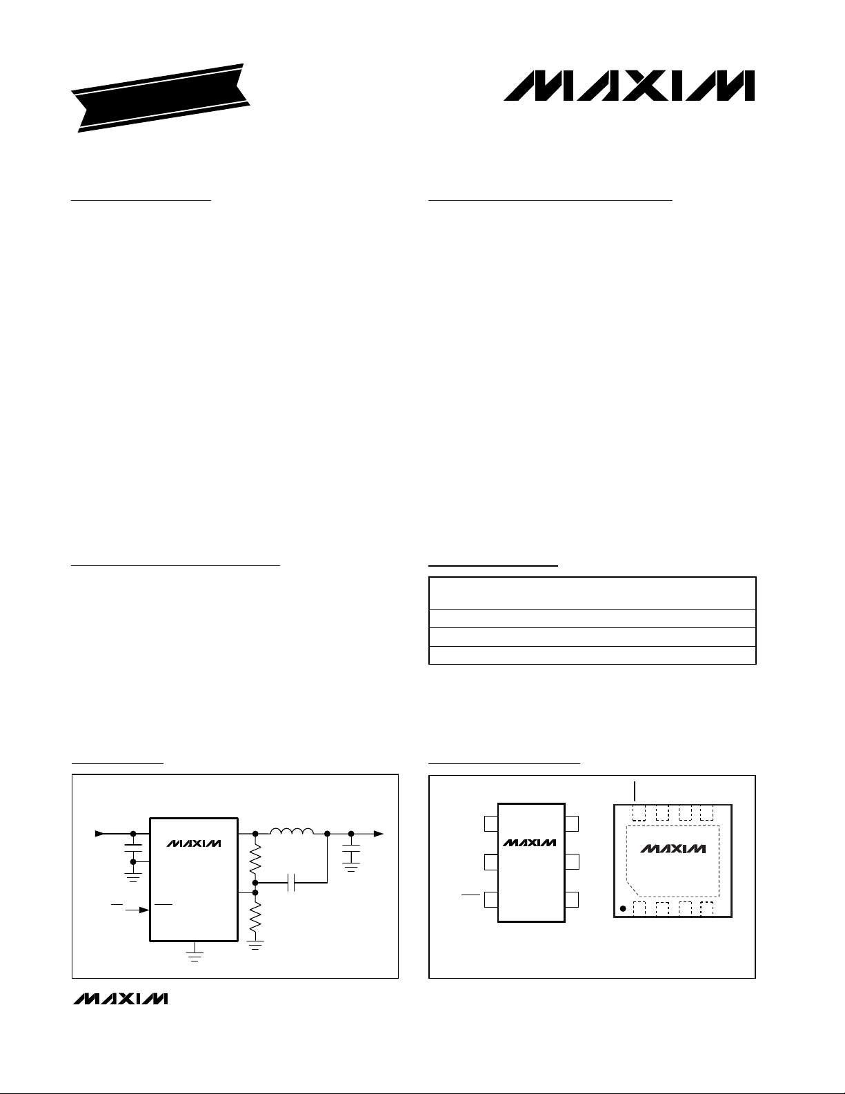
GND
IN
LX
FB
SHDNON/OFF
OUTPUT
0.6V TO 2.5V
UP TO 500mA
INPUT
2.7V TO 5.5V
L
1µH
C
OUT
2.2µF
C
IN
2.2µF
C
FF
R1
R2
MAX8560
PGND
Typical Operating Circuit
19-2954; Rev 0; 7/03
For pricing, delivery, and ordering information, please contact Maxim/Dallas Direct! at
1-888-629-4642, or visit Maxim’s website at www.maxim-ic.com.
EVALUATION KIT
AVAILABLE
Pin Configurations
*Future product—contact factory for availability.
PART TEMP RANGE PIN-PACKAGE
MAX8560EUT* -40°C to +85°C 6 SOT23-6 ABRY
MAX8561ETA -40°C to +85°C 8 TDFN AHD
MAX8562ETA -40°C to +85°C 8 TDFN AHE
TOP
MARK
TOP VIEW
16LXIN
MAX8560
2
GND
34
SOT23-6
GND
76
MAX8561/
MAX8562
2
PGND
TDFN
FB
3
LX
5 PGND
FBSHDN
SHDN
8
1
IN
3mm × 3mm × 0.8mm
ODO
5
4
ODI
Page 2

MAX8560/MAX8561/MAX8562
4MHz, 500mA Synchronous Step-Down
DC-DC Converters in SOT and TDFN
2 _______________________________________________________________________________________
ABSOLUTE MAXIMUM RATINGS
Stresses beyond those listed under “Absolute Maximum Ratings” may cause permanent damage to the device. These are stress ratings only, and functional
operation of the device at these or any other conditions beyond those indicated in the operational sections of the specifications is not implied. Exposure to
absolute maximum rating conditions for extended periods may affect device reliability.
IN, FB, SHDN, ODI, ODO to GND ............................-0.3V to +6V
LX to GND (Note 1)......................................-0.3V to (V
IN
+ 0.3V)
PGND to GND .......................................................-0.3V to +0.3V
LX Current ...........................................................................1.27A
Output Short Circuit to GND
(typical operating circuit)....................................................10s
Continuous Power Dissipation (T
A
= +70°C)
6-Pin SOT23 (derate 8.7mW/°C above +70°C)............695mW
8-Pin TDFN (derate 24.4mW/°C above +70°C) .........1951mW
Operating Temperature Range ...........................-40°C to +85°C
Junction Temperature......................................................+150°C
Storage Temperature Range .............................-65°C to +150°C
Lead Temperature (soldering, 10s) .................................+300°C
ELECTRICAL CHARACTERISTICS
(VIN= 3.6V, SHDN = IN, TA= -40°C to +85°C, typical values are at TA= +25°C, unless otherwise noted.) (Note 1)
Note 1: LX has internal clamp diodes to PGND and IN. Applications that forward bias these diodes should take care not to exceed
the IC’s package power-dissipation limits.
Supply Voltage Range V
UVLO Threshold UVLO VIN rising, 60mV hysteresis 2.4 2.5 2.6 V
Supply Current I
Output Voltage Range V
FB Threshold Voltage V
FB Threshold Line Regulation VIN = 2.7V to 5.5V 0.3 % / V
FB Threshold Load Regulation I
FB Threshold Voltage Accuracy
(Falling) (% of V
FB Threshold Voltage Hysteresis
(% of V
FB Bias Current I
Logic Input High Voltage
(SHDN, ODI)
Logic Input Low Voltage
(SHDN, ODI)
Logic Input Bias Current IIH, I
ODO Output Low Voltage
(MAX8562 Only)
PARAMETER SYMBOL CONDITIONS MIN TYP MAX UNITS
IN
I
= 0mA, no switching 40 80
LOAD
IN
SHDN = GND
OUT
VFB falling 0.6 V
FB
= 0 to 500mA -0.001 %/mA
OUT
I
= 0mA
LOAD
SHDN = GND, TA = +25°C, VIN = 5.5V 0.01 0.1
SHDN = GND, TA = +85°C, VIN = 5.5V 0.1
VFB = 0.5V, TA = +25°C, VIN = 5.5V 0.01 0.1
VFB = 0.5V, TA = +85°C, VIN = 5.5V 0.1
VIN = 2.7V to 5.5V 1.41
VIN = 2.7V to 5.5V 0.4
VIN = 5.5V, SHDN = ODI = GND or IN,
T
= +25°C
A
IL
VIN = 5.5V, SHDN = ODI = GND or IN,
= +85°C
T
A
1mA sink current, VIN = 2.7V 0.02 0.1 V
FB
)
FB
V
)
HYS
V
V
V
FB
IH
IL
OL
2.7 5.5 V
TA = +25°C 0.01 0.1
T
= +85°C 0.1
A
0.6 2.5 V
TA = +25°C -1.5 +1.5
T
= -40°C to +85°C -2.5 +2.5
A
1.0 %
0.001 0.1
0.01
µA
%
%
µA
V
µA
Page 3
MAX8560/MAX8561/MAX8562
4MHz, 500mA Synchronous Step-Down
DC-DC Converters in SOT and TDFN
_______________________________________________________________________________________ 3
ELECTRICAL CHARACTERISTICS (continued)
(VIN= 3.6V, SHDN = IN, TA= -40°C to +85°C, typical values are at TA= +25°C, unless otherwise noted.) (Note 1)
)
)
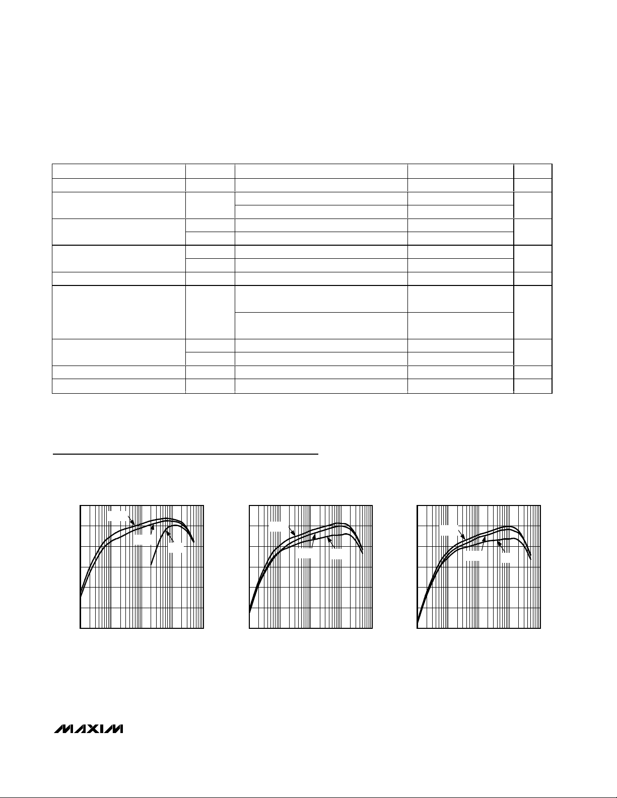
Typical Operating Characteristics
(VIN= 3.6V, V
OUT
= 1.2V, L = 1µH (LQH32C-IRO), C
OUT
= 2.2µF, TA= +25°C, unless otherwise noted.)
EFFICIENCY vs. LOAD CURRENT
(V
OUT
= 2.5V)
MAX8560 toc01
LOAD CURRENT (mA)
EFFICIENCY (%)
100101
50
60
70
80
90
100
40
0.1 1000
4.7µH
2.2µH
1µH
EFFICIENCY vs. LOAD CURRENT
(V
OUT
= 1.8V)
MAX8560 toc02
LOAD CURRENT (mA)
EFFICIENCY (%)
100101
50
60
70
80
90
100
40
0.1 1000
4.7µH
2.2µH
1µH
EFFICIENCY vs. LOAD CURRENT
(V
OUT
= 1.5V)
MAX8560 toc03
LOAD CURRENT (mA)
EFFICIENCY (%)
100101
50
60
70
80
90
100
40
0.1 1000
4.7µH
2.2µH
1µH
ODO Pullup to IN (MAX8562 Only) 5 10 20 kΩ
Open-Drain Output Leakage I
Current Limit
On-Resistance
Rectifier-Off Current Threshold I
LX Leakage Current I
Minimum On- and Off-Times
Thermal Shutdown +160 °C
Thermal-Shutdown Hysteresis 20 °C
PARAMETER SYMBOL CONDITIONS MIN TYP MAX UNITS
OHLEAK
I
LIMP
I
LIMN
R
ONP
R
ONN
LXOFF
LXLKG
t
ON(MIN
t
OFF(MIN
VIN = 5.5V, ODO = IN, TA = +25°C 0.01 0.1
VIN = 5.5V, ODO = IN, TA = +85°C 0.1
PFET switch 600 990 1500
NFET rectifier 490 680 900
PFET switch, ILX = -40mA 0.8 1.5
NFET rectifier, ILX = +40mA 0.4 0.82
03060mA
V
= 5.5V, LX = GND to IN, ODO = IN,
IN
T
= +25°C, SHDN = GND
A
V
= 5.5V, LX = GND to IN, ODO = IN,
IN
T
= +85°C, SHDN = GND
A
0.1 1
1
107
95
µA
mA
Ω
µA
ns
Page 4

MAX8560/MAX8561/MAX8562
4MHz, 500mA Synchronous Step-Down
DC-DC Converters in SOT and TDFN
4 _______________________________________________________________________________________
Typical Operating Characteristics (continued)
(VIN= 3.6V, V
OUT
= 1.2V, L = 1µH (LQH32C-IRO), C
OUT
= 2.2µF, TA= +25°C, unless otherwise noted.)
100
90
80
70
EFFICIENCY (%)
60
EFFICIENCY vs. LOAD CURRENT
= 1.2V)
(V
OUT
4.7µH
2.2µH
1µH
MAX8560 toc04
EFFICIENCY vs. LOAD CURRENT
100
90
80
70
EFFICIENCY (%)
60
EFFICIENCY vs. LOAD CURRENT
= 0.9V)
(V
4.7µH
OUT
2.2µH
1µH
MAX8560 toc05
100
90
80
70
EFFICIENCY (%)
60
4.7µH
(LOAD = 7.5Ω)
2.2µH
MAX8560 toc06
1µH
50
40
0.1 1000
LOAD CURRENT (mA)
100101
NO-LOAD SUPPLY CURRENT
vs. SUPPLY VOLTAGE
47
46
45
44
43
42
SUPPLY CURRENT (µA)
41
40
39
2.0 5.5
SUPPLY VOLTAGE (V)
R1 = R2 = 100kΩ
5.04.52.5 3.0 3.5 4.0
LIGHT-LOAD SWITCHING WAVEFORMS
50mA LOAD
MAX8560 toc07
MAX8560 toc10
50
40
0.1 1000
LOAD CURRENT (mA)
SWITCHING FREQUENCY
vs. LOAD CURRENT
10
1µH
1
FREQUENCY (MHz)
0.1
0500
100 200 300 400
V
OUT
20mV/div
I
L
200mA/div
0
2.2µH
LOAD CURRENT (mA)
50
100101
40
0.5 2.5
OUTPUT VOLTAGE vs. LOAD CURRENT
1.24
1.23
MAX8560 toc08
1.22
1.21
1.20
4.7µH
1.19
OUTPUT VOLTAGE (V)
1.18
1.17
1.16
0500
HEAVY-LOAD SWITCHING WAVEFORMS
2.01.51.0
OUTPUT VOLTAGE (V)
(VOLTAGE POSITIONING)
R1 = R2 = 100kΩ
LOAD CURRENT (mA)
MAX8560 toc11
200mA LOAD
V
OUT
20mV/div
I
L
200mA/div
0
MAX8560 toc09
400300100 200
V
LX
2V/div
200ns/div
200ns/div
V
LX
2V/div
Page 5

MAX8560/MAX8561/MAX8562
4MHz, 500mA Synchronous Step-Down
DC-DC Converters in SOT and TDFN
_______________________________________________________________________________________ 5
Typical Operating Characteristics (continued)
(VIN= 3.6V, V
OUT
= 1.2V, L = 1µH (LQH32C-IRO), C
OUT
= 2.2µF, TA= +25°C, unless otherwise noted.)
LIGHT-LOAD SOFT-START WAVEFORMS
100Ω LOAD
LOAD TRANSIENT RESPONSE
20mA LOAD
MAX8560 toc12
20µs/div
MAX8560 toc15
500mA LOAD
20mA LOAD
2µs/div
V
OUT
1V/div
I
IN
200mA/div
I
L
200mA/div
0
V
SHDN
2V/div
V
OUT
50mV/div
I
L
500mA/div
0
I
LOAD
500mA/div
HEAVY-LOAD SOFT-START WAVEFORMS
3Ω LOAD
20µs/div
MAX8560 toc13
OUTPUT-VOLTAGE TRANSIENT RESPONSE
(MAX8561)
V
OUT
V
= 1.0V
OUT
7.5Ω LOAD, L = 2.2µH
40µs/div
= 1.5V
MAX8560 toc16
V
OUT
1V/div
I
IN
200mA/div
I
L
200mA/div
0
V
SHDN
2V/div
V
OUT
500mV/div
I
L
200mA/div
0
V
ODI
2V/div
LINE-TRANSIENT RESPONSE
5Ω LOAD
VIN = 4.0V
VIN = 3.5V
2µs/div
MAX8560 toc14
BYPASS-FET TRANSIENT RESPONSE
7.5Ω LOAD
V
= 1.2V
OUT
(MAX8562)
V
= V
OUT
IN
20µs/div
MAX8560 toc17
V
OUT
20mV/div
I
L
200mA/div
0
V
IN
500mV/div
V
OUT
2V/div
0
I
L
500mA/div
0
V
ODI
2V/div
Page 6

MAX8560/MAX8561/MAX8562
4MHz, 500mA Synchronous Step-Down
DC-DC Converters in SOT and TDFN
6 _______________________________________________________________________________________
Detailed Description
The MAX8560/MAX8561/MAX8562 step-down converters
deliver a guaranteed 500mA at output levels from 0.6V to
2.5V. They use a proprietary hysteretic-PWM control
scheme that switches up to 4MHz, allowing a trade-off
between efficiency and tiny external components. At light
loads below 100mA, the MAX8560/MAX8561/MAX8562
automatically switch to pulse-skipping mode to keep quiescent supply current as low as 40µA (typ).
Control Scheme
A proprietary hysteretic-PWM control scheme ensures
high efficiency, fast switching, fast transient response,
low output ripple, and physically tiny external components. This control scheme is simple: when the output
voltage falls below the regulation threshold, the error
comparator begins a switching cycle by turning on the
high-side switch. This switch remains on until the minimum on-time expires and the output voltage is in regulation or the current-limit threshold is exceeded. Once
off, the high-side switch remains off until the minimum
off-time expires and the output voltage falls again,
below the regulation threshold. During this period, the
low-side synchronous rectifier turns on and remains on
until either the high-side switch turns on again or the
inductor current approaches zero. The internal synchronous rectifier eliminates the need for an external
Schottky diode.
Voltage-Positioning Load Regulation
As seen in the Typical Operating Circuit, the
MAX8560/MAX8561/MAX8562 use a unique feedback
network. By taking feedback from the LX node through
R1, the usual phase lag due to the output capacitor is
removed, making the loop exceedingly stable and
allowing the use of a very small ceramic output capacitor. This configuration causes the output voltage to shift
by the inductor series resistance multiplied by the load
current. This voltage-positioning load regulation greatly
reduces overshoot during load transients, which effectively halves the peak-to-peak output-voltage excursions compared to traditional step-down converters.
See the Load Transient Response graph in the Typical
Operating Characteristics section.
Pin Description
PIN
MAX8560
11IN
2 7 GND Analog Ground
38SHDN
46FB
5 2 PGND Power Ground. Must connect to GND.
6 3 LX Inductor connection to the drains of the internal P-channel and N-channel MOSFETs.
— 5 ODO Auxiliary Open-Drain Output
— 4 ODI
— EP EP Exposed Pad. Connect to GND.
MAX8561
MAX8562
NAME FUNCTION
Supply Voltage Input. 2.7V to 5.5V. Bypass with a 2.2µF ceramic capacitor as close as
possible to the IN and GND pins.
Active-Low Shutdown Input. Connect to IN or logic high for normal operation. Connect to
GND or logic low for shutdown mode.
Voltage Feedback Input. FB regulates to 0.6V nominal. Connect FB to the center of an
external resistive divider (see the Setting the Output Voltage section).
Digital Input for Open-Drain MOSFET. Connect to IN or logic high to internally pull ODO
low (and force the MAX8562 into 100% duty cycle). Connect to GND or logic low to force
ODO to high impedance (MAX8561) or 10kΩ pullup from ODO to IN (MAX8562).
Page 7

MAX8560/MAX8561/MAX8562
4MHz, 500mA Synchronous Step-Down
DC-DC Converters in SOT and TDFN
_______________________________________________________________________________________ 7
Shutdown Mode
Connecting SHDN to GND or logic low places the
MAX8560/MAX8561/MAX8562 in shutdown mode and
reduces supply current to 0.1µA. In shutdown, the control circuitry, internal-switching P-channel MOSFET, and
synchronous rectifier (N-channel MOSFET) turn off and
LX becomes high impedance. Connect SHDN to IN or
logic high for normal operation.
Soft-Start
The MAX8560/MAX8561/MAX8562 have internal softstart circuitry that eliminates inrush current at startup,
reducing transients on the input source. Soft-start is particularly useful for higher impedance input sources,
such as Li+ and alkaline cells. See the Soft-Start and
Shutdown Response graphs in the Typical Operating
Characteristics section.
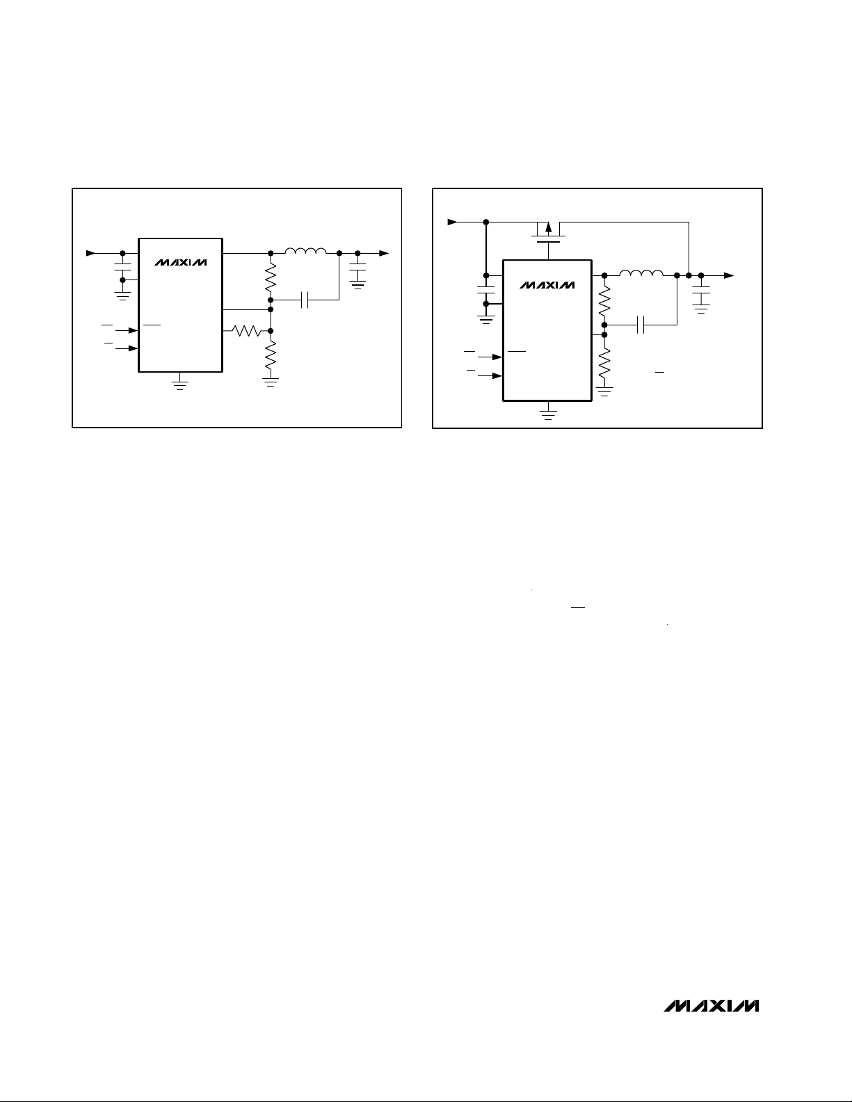
Open-Drain Output
The 8-pin TDFN versions, the MAX8561 and MAX8562,
include an extra, internal, open-drain N-channel MOSFET
switch that can save an additional package in space-constrained applications. The open drain is connected to
ODO, while the gate is controlled by a digital input at
ODI. For the MAX8561, this circuit can be used to toggle
between two regulated output voltages, as in Figure 2.
For the MAX8562, a 10kΩ resistor pulls ODO up to IN
when ODI is low, and the buck converter is forced into
100% duty cycle when ODI is high. This makes the
MAX8562 ideal for driving an external bypass PFET for
high-power mode in CDMA cell phones, as in Figure 3.
Applications Information
The MAX8560/MAX8561/MAX8562 are optimized for
use with tiny inductors and small ceramic capacitors.
The correct selection of external components, especially C
FF
, ensures high efficiency, low output ripple, and
fast transient response.
Setting the Output Voltage
Select an output voltage between 0.6V and 2.5V by
connecting FB to a resistive voltage-divider between LX
and GND (see the Typical Operating Circuit). Choose
R2 for a reasonable bias current in the resistive divider.
A wide range of resistor values is acceptable, but a
good starting point is to choose R2 as 100kΩ. Then, R1
is given by:
where V
FB
= 0.6V.
Inductor Selection
The MAX8560/MAX8561/MAX8562 operate with inductors
of 1µH to 4.7µH. Low inductance values are smaller but
require faster switching, which results in some efficiency
loss. See the Typical Operating Characteristics section
for efficiency and switching frequency vs. inductor value.
The inductor’s DC current rating only needs to match the
maximum load current of the application + 50mA
because the MAX8560/MAX8561/ MAX8562 feature zero
current overshoot during startup and load transients.
For output voltages above 2.0V, when light-load efficiency is important, the minimum recommended inductor is
2.2µH. For optimum voltage-positioning load transients,
choose an inductor with DC series resistance in the
50mΩ to 150mΩ range. For higher efficiency at heavy
loads (above 200mA) or minimal load regulation (but
some transient overshoot), the resistance should be kept
below 100mΩ. For light-load applications up to 200mA,
much higher resistance is acceptable with very little
impact on performance.
RR
V
V
OUT
FB
12 1=−
Figure 1. Simplified Functional Diagram
IN
PFET
SHDN
MAX8561*
MAX8562*
ODI
PWM
LOGIC
MAX8560
*NOTE: ODI/ODO AVAILABLE IN THE MAX8561/MAX8562 ONLY.
THE MAX8561 ODO IS AN OPEN-DRAIN OUTPUT. THE MAX8562
HAS AN INTERNAL 10kΩ PULLUP TO IN.
NFET
0.6V
10kΩ
GND
LX
PGND
FB
ODO
Page 8
MAX8560/MAX8561/MAX8562
4MHz, 500mA Synchronous Step-Down
DC-DC Converters in SOT and TDFN
8 _______________________________________________________________________________________
Capacitor Selection
Output Capacitor
The output capacitor, C
OUT
, is required to keep the
output voltage ripple small and to ensure regulation
loop stability. C
OUT
must have low impedance at the
switching frequency. Ceramic capacitors with X5R or
X7R dielectrics are highly recommended due to their
small size, low ESR, and small temperature coefficients.
Due to the unique feedback network, the output capacitance can be very low. For most applications, a 2.2µF
capacitor is sufficient. For optimum load-transient performance and very low output ripple, the output capacitor value in µFs should be equal to or larger than the
inductor value in µHs.
Input Capacitor
The input capacitor, C
IN
, reduces the current peaks
drawn from the battery or input power source and
reduces switching noise in the IC. The impedance of
CINat the switching frequency should be kept very low.
Ceramic capacitors with X5R or X7R dielectrics are
highly recommended due to their small size, low ESR,
and small temperature coefficients. Due to the
MAX8560/MAX8561/MAX8562s’ soft-start, the input
capacitance can be very low. For most applications, a
2.2µF capacitor is sufficient.
Feed-Forward Capacitor
The feed-forward capacitor, C
FF
, sets the feedback loop
response, controls the switching frequency, and is critical in obtaining the best efficiency possible. Choose a
small ceramic X7R capacitor with a value given by:
Select the closest standard value to CFFas possible.
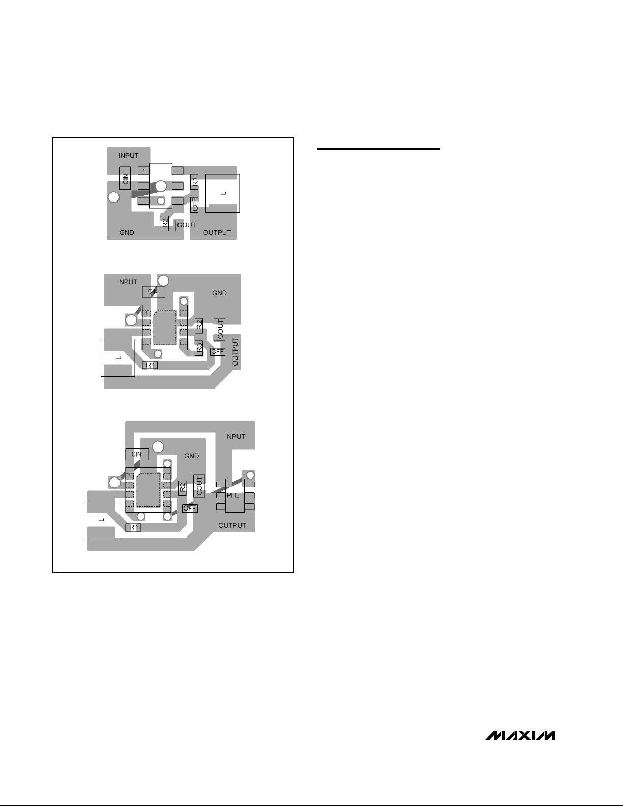
PC Board Layout and Routing
High switching frequencies and relatively large peak currents make the PC board layout a very important part of
design. Good design minimizes excessive EMI on the
feedback paths and voltage gradients in the ground
plane, both of which can result in instability or regulation
errors. Connect CINas close as possible to IN and GND.
Connect the inductor and output capacitor as close to
the IC as possible and keep their traces short, direct,
and wide. Connect GND and PGND separately to the
ground plane. The external feedback network should be
very close to the FB pin, within 0.2in (5mm). Keep noisy
traces, such as the LX node, as short as possible. For
the 8-pin TDFN package, connect GND to the exposed
paddle directly under the IC. Figure 4 illustrates an
example PC board layout and routing scheme.
C
L
R
Siemens
FF
=×110
Figure 2. Using ODI/ODO to Obtain Two Output Voltages from
the MAX8561
Figure 3. Using the MAX8562 to Control an External Bypass
PFET for a Two-Step V
CC
in CDMA-PA Applications
INPUT
Li+ BATTERY
HP/LP
IN
GND
SHDNON/OFF
ODI
ODO
MAX8562
PGND
PFET
LX
100kΩ
FB
100kΩ
INPUT
Li+ BATTERY
1.5/1.0
IN
GND
SHDNON/OFF
ODI
MAX8561
PGND
ODO
OUTPUT
LX
FB
120kΩ
2.2µH
100kΩ
220pF
150kΩ
1.5V OR 1.0V
AT 500mA
2.2µF2.2µF
1.5µH
150pF
HP = HIGH-POWER MODE
LP = LOW-POWER MODE
OUTPUT
1.2V OR V
2.2µF2.2µF
BATT
Page 9

MAX8560/MAX8561/MAX8562
4MHz, 500mA Synchronous Step-Down
DC-DC Converters in SOT and TDFN
_______________________________________________________________________________________ 9
Table 1. Suggested Inductors
MANUFACTURER SERIES
LB2012
LB2016
Taiyo Yuden
Murata
TOKO
LB2518
LBC2518
LQH31C_03 1.0 0.28 510 3.2 x 1.6 x 2.0 = 10mm
LQH32C_53
LQM43FN
D310F
D312C
INDUCTANCE
(µH)
1.0
2.2
1.0
1.5
2.2
3.3
1.0
1.5
2.2
3.3
1.0
1.5
2.2
3.3
4.7
1.0
2.2
4.7
2.2
4.7
1.5
2.2
3.3
1.5
2.2
2.7
3.3
ESR
(Ω)
0.15
0.23
0.09
0.11
0.13
0.20
0.06
0.07
0.09
0.11
0.08
0.11
0.13
0.16
0.20
0.06
0.10
0.15
0.10
0.17
0.13
0.17
0.19
0.10
0.12
0.15
0.17
CURRENT RATING
(mA)
300
240
455
350
315
280
500
400
340
270
775
660
600
500
430
1000
790
650
400
300
1230
1080
1010
1290
1140
980
900
DIMENSIONS
2.0 x 1.25 x 1.45 = 3.6mm
2.0 x 1.6 x 1.8 = 5.8mm
2.5 x 1.8 x 2.0 = 9mm
2.5 x 1.8 x 2.0 = 9mm
3.2 x 2.5 x 1.7 = 14mm
4.5 x 3.2 x 0.9 = 13mm
3.6 x 3.6 x 1.0 = 13mm
3.6 x 3.6 x 1.2 = 16mm
3
3
3
3
3
3
3
3
3
Sumida CDRH2D11
1.5
2.2
3.3
4.7
0.05
0.08
0.10
0.14
900
780
600
500
3.2 x 3.2 x 1.2 = 12mm
3
Page 10
MAX8560/MAX8561/MAX8562
4MHz, 500mA Synchronous Step-Down
DC-DC Converters in SOT and TDFN
10 ______________________________________________________________________________________
Figure 4. Recommended PC Board Layout
Chip Information
TRANSISTOR COUNT: 1271
PROCESS: BiCMOS
(a) MAX8560
(b) MAX8561
(c) MAX8562
Page 11

MAX8560/MAX8561/MAX8562
4MHz, 500mA Synchronous Step-Down
DC-DC Converters in SOT and TDFN
______________________________________________________________________________________ 11
Package Information
(The package drawing(s) in this data sheet may not reflect the most current specifications. For the latest package outline information,
go to www.maxim-ic.com/packages
.)
6LSOT.EPS
PACKAGE OUTLINE, SOT-23, 6L
1
21-0058
F
1
Page 12

MAX8560/MAX8561/MAX8562
4MHz, 500mA Synchronous Step-Down
DC-DC Converters in SOT and TDFN
Maxim cannot assume responsibility for use of any circuitry other than circuitry entirely embodied in a Maxim product. No circuit patent licenses are
implied. Maxim reserves the right to change the circuitry and specifications without notice at any time.
12 ____________________Maxim Integrated Products, 120 San Gabriel Drive, Sunnyvale, CA 94086 408-737-7600
© 2003 Maxim Integrated Products Printed USA is a registered trademark of Maxim Integrated Products.
Package Information (continued)
(The package drawing(s) in this data sheet may not reflect the most current specifications. For the latest package outline information,
go to www.maxim-ic.com/packages
.)
PIN 1
INDEX
AREA
D
E
A
A2
b
E2
DETAIL A
e
D2
C0.35
L
PIN 1 ID
1N1
[(N/2)-1] x e
REF.
6, 8, &10L, QFN THIN.EPS
A1
C
L
L
e
A
NUMBER OF LEADS SHOWN ARE FOR REFERENCE ONLY
COMMON DIMENSIONS
MIN. MAX.
SYMBOL
0.70 0.80
A
2.90 3.10
D
E
2.90 3.10
0.00 0.05
A1
L
0.20 0.40
k
0.25 MIN.
A2 0.20 REF.
PACKAGE VARIATIONS
PKG. CODE
T633-1 1.50–0.10D22.30–0.10
N
6
1.50–0.10
E2
2.30–0.10T833-1 8
JEDEC SPEC
0.95 BSCeMO229 / WEEA
MO229 / WEEC
0.65 BSC
DALLAS
SEMICONDUCTOR
PROPRIETARY INFORMATION
TITLE:
PACKAGE OUTLINE, 6, 8 & 10L,
TDFN, EXPOSED PAD, 3x3x0.80 mm
APPROVAL
[(N/2)-1] x e
0.40–0.05b1.90 REF
1.95 REF0.30–0.05
0.25–0.05 2.00 REFMO229 / WEED-30.50 BSC1.50–0.10 2.30–0.1010T1033-1
k
C
L
L
e
DOCUMENT CONTROL NO. REV.
21-0137 D
1
2
DALLAS
SEMICONDUCTOR
PROPRIETARY INFORMATION
TITLE:
PACKAGE OUTLINE, 6, 8 & 10L,
TDFN, EXPOSED PAD, 3x3x0.80 mm
DOCUMENT CONTROL NO.APPROVAL
21-0137
REV.
2
2
D
 Loading...