

Page 1
General Description
The MAX8545/MAX8546/MAX8548 are voltage-mode
pulse-width-modulated (PWM), step-down DC-DC controllers ideal for a variety of cost-sensitive applications.
They drive low-cost N-channel MOSFETs for both the
high-side switch and synchronous rectifier, and require
no external current-sense resistor. These devices can
supply output voltages as low as 0.8V.
The MAX8545/MAX8546/MAX8548 have a wide 2.7V to
28V input range, and do not need any additional bias
voltage. The output voltage can be precisely regulated
from 0.8V to 0.83 x VIN. These devices can provide efficiency up to 95%. Lossless short-circuit and current-limit
protection is provided by monitoring the R
DS(ON)
of the
low-side MOSFET. The MAX8545 and MAX8548 have a
current-limit threshold of 320mV, while the MAX8546 has
a current-limit threshold of 165mV. All devices feature
foldback-current capability to minimize power dissipation
under short-circuit condition. Pulling the COMP/EN pin
low with an open-collector or low-capacitance, opendrain device can shut down all devices.
The MAX8545/MAX8546 operate at 300kHz and the
MAX8548 operates at 100kHz. The MAX8545/
MAX8546/MAX8548 are compatible with low-cost aluminum electrolytic capacitors. Input undervoltage lockout prevents proper operation under power-sag
operations to prevent external MOSFETs from overheating. Internal soft-start is included to reduce inrush current. These devices are offered in space-saving 10-pin
µMAX packages.
Applications
Features
♦ 2.7V to 28V Input Range
♦ Foldback Short-Circuit Protection
♦ No Additional Bias Supply Needed
♦ 0.8V to 0.83 x V
IN
Output
♦ Up to 95% Efficiency
♦ Low-Cost External Components
♦ No Current-Sense Resistor
♦ All N-Channel MOSFET Design
♦ Adaptive Gate Drivers Eliminate Shoot-Through
♦ Lossless Overcurrent and Short-Circuit
Protection
♦ 300kHz Switching Frequency
(MAX8545/MAX8546)
♦ 100kHz Switching Frequency (MAX8548)
♦ Pin-Compatible with the MAX1967
♦ Thermal Shutdown
MAX8545/MAX8546/MAX8548
Low-Cost, Wide Input Range, Step-Down
Controllers with Foldback Current Limit
________________________________________________________________ Maxim Integrated Products 1
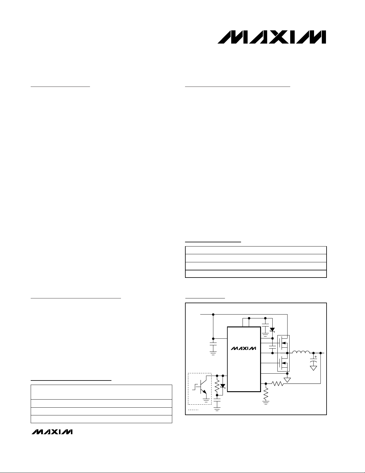
Typical Operating Circuit
Ordering Information
Pin Configuration appears at end of data sheet.
19-2795; Rev 0; 7/03
For pricing, delivery, and ordering information, please contact Maxim/Dallas Direct! at
1-888-629-4642, or visit Maxim’s website at www.maxim-ic.com.
Selector Guide
Set-Top Boxes
Graphic Card and Video
Supplies
Desktops and Desknotes
PCI Express Power
Supplies
Telecom Power Supplies
Notebook Docking
Station Supplies
Cable Modems and
Routers
Networking Power
Supplies
PART TEMP RANGE PIN-PACKAGE
MAX8545EUB -40°C to +85°C 10 µMAX
MAX8546EUB -40°C to +85°C 10 µMAX
MAX8548EUB -40°C to +85°C 10 µMAX
PART
MAX8545 300kHz -320mV
MAX8546 300kHz -165mV
MAX8548 100kHz -320mV
SWITCHING
FREQUENCY
CURRENT-LIMIT
THRESHOLD
2.7V TO 28V
OFF
ON
OPTIONAL
INPUT
VLV
CC
IN
COMP/
EN
MAX8545
MAX8546
MAX8548
BSTV
GND
DH
LX
DL
FB
OUTPUT
0.8V TO
0.9 x V
UP TO 6A
IN
Page 2
MAX8545/MAX8546/MAX8548
Low-Cost, Wide Input Range, Step-Down
Controllers with Foldback Current Limit
2 _______________________________________________________________________________________
ABSOLUTE MAXIMUM RATINGS
ELECTRICAL CHARACTERISTICS
(VIN= VL= VCC= 5V, TA= -40°C to +85°C, unless otherwise noted. Typical values are at TA= +25°C.)
Stresses beyond those listed under “Absolute Maximum Ratings” may cause permanent damage to the device. These are stress ratings only, and functional
operation of the device at these or any other conditions beyond those indicated in the operational sections of the specifications is not implied. Exposure to
absolute maximum rating conditions for extended periods may affect device reliability.
(All voltages referenced to GND unless otherwise noted.)
V
IN
to GND ............................................................-0.3V to +30V
V
CC
to GND .............................-0.3V, lower of 6V or (VL + 0.3V)
FB to GND ................................................................-0.3V to +6V
BST to GND ............................................................-0.3V to +36V
VL, DL, COMP to GND ..............................-0.3V to (V
CC
+ 0.3V)
BST to LX..................................................................-0.3V to +6V
DH to LX....................................................-0.3V to (V
BST
+ 0.3V)
VL Short to GND ......................................................................5s
LX to GND ......................................................................0 to 30V
Input Current (any pin) .....................................................±50mA
Continuous Power Dissipation (T
A
= +70°C)
10-Pin µMAX (derate 5.6mW/°C above +70°C) ..........444mW
Operating Temperature Range ...........................-40°C to +85°C
Junction Temperature......................................................+150°C
Storage Temperature Range .............................-65°C to +150°C
Lead Temperature (soldering, 10s) .................................+300°C
VIN Operating Range V
VIN Undervoltage Lockout
(UVLO) Trip Level
VIN Operating Supply Current VFB = 0.88V (no switching)
VL Output Voltage
Thermal Shutdown
OSCILLATOR
Frequency f
Minimum Duty Cycle DC
Maximum Duty Cycle DC
SOFT-START
Digital Ramp Period
Soft-Start Levels
PARAMETER SYMBOL CONDITIONS MIN TYP MAX UNITS
VCC = VL, VIN separate from V
IN
VIN = VL = V
Rising and falling edge, hysteresis = 2% 2.35 2.50 2.66 V
OSC
MIN
MAX
5.5V < V
1mA < I
Rising temperature, typical
hysteresis = 10°C (Note 1)
MAX8545, MAX8546 250 300 360
MAX8548 80 100 120
DH output, MAX8545, MAX8546 5
MAX8548 10
DH output, MAX8545, MAX8546 83 86
MAX8548 90 95
MAX8545, MAX8546 6.6
MAX8548
MAX8545, MAX8546 V
MAX8548
< 28V, VCC = VL,
IN
LOAD
CC
CC
< 25mA
4.9 28.0
2.7 5.5
0.7
4.7 5 5.3 V
+160 °C
10.2
/ 64
OUT
V
/ 32
OUT
1.2 mA
V
kHz
%
%
ms
V
Page 3

MAX8545/MAX8546/MAX8548
Low-Cost, Wide Input Range, Step-Down
Controllers with Foldback Current Limit
_______________________________________________________________________________________ 3
ELECTRICAL CHARACTERISTICS (continued)
(VIN= VL= VCC= 5V, TA= -40°C to +85°C, unless otherwise noted. Typical values are at TA= +25°C.)
Note 1: Thermal shutdown disables the buck regulator when the die reaches this temperature. Soft-start is reset but the VL regulator
remains on.
ERROR AMPLIFIER
FB Regulation Voltage
FB to COMP/EN Gain
FB to COMP/EN
Transconductance
FB Input Bias Current V
COMP/EN Source Current V
Current-Limit Threshold Voltage
(Across Low-Side MOSFET)
Foldback Current-Limit Threshold
Voltage (Across Low-Side
MOSFET) When Output is Short
MOSFET DRIVERS
Break-Before-Make Time
DH On-Resistance in Low State 1.6 4 Ω
DH On-Resistance in High State 2.5 5.5 Ω
DL On-Resistance in Low State 1.1 2.5 Ω
DL On-Resistance in High State 2.5 5.5 Ω
BST Leakage Current V
LX Leakage Current V
PARAMETER SYMBOL CONDITIONS MIN TYP MAX UNITS
2.7V < VCC < 5.5V, 0°C to +85°C 0.787 0.800 0.815
2.7V < V
-5µA < I
FB
COMP/EN
LX to GND, MAX8545, MAX8548,
V
FB
LX to GND MAX8546, V
LX to GND, VFB = 0V,
MAX8545, MAX8548
MAX8546, LX to GND, V
Rising edge, DH going low to DL going high 96
Falling edge, DL going low to DH going high 28
BST
BST
< 5.5V, -40°C to +85°C 0.782 0.800 0.815
CC
4000 V / V
COMP/EN
= 0.88V 1 2 µA
= 0.8V
= 33V, V
= 33V, V
< +5µA 70 108 160 µS
= 0V 15 46 100 µA
-355 -320 -280
= 0.8V -185 -165 -140
FB
-105 -75 -45
= 0 -53 -38 -22
FB
= 28V, VFB = 0.88V 0 50 µA
LX
= 28V, VFB = 0.88V 33 100 µA
LX
V
mV
mV
ns
Page 4

MAX8545/MAX8546/MAX8548
Low-Cost, Wide Input Range, Step-Down
Controllers with Foldback Current Limit
4 _______________________________________________________________________________________
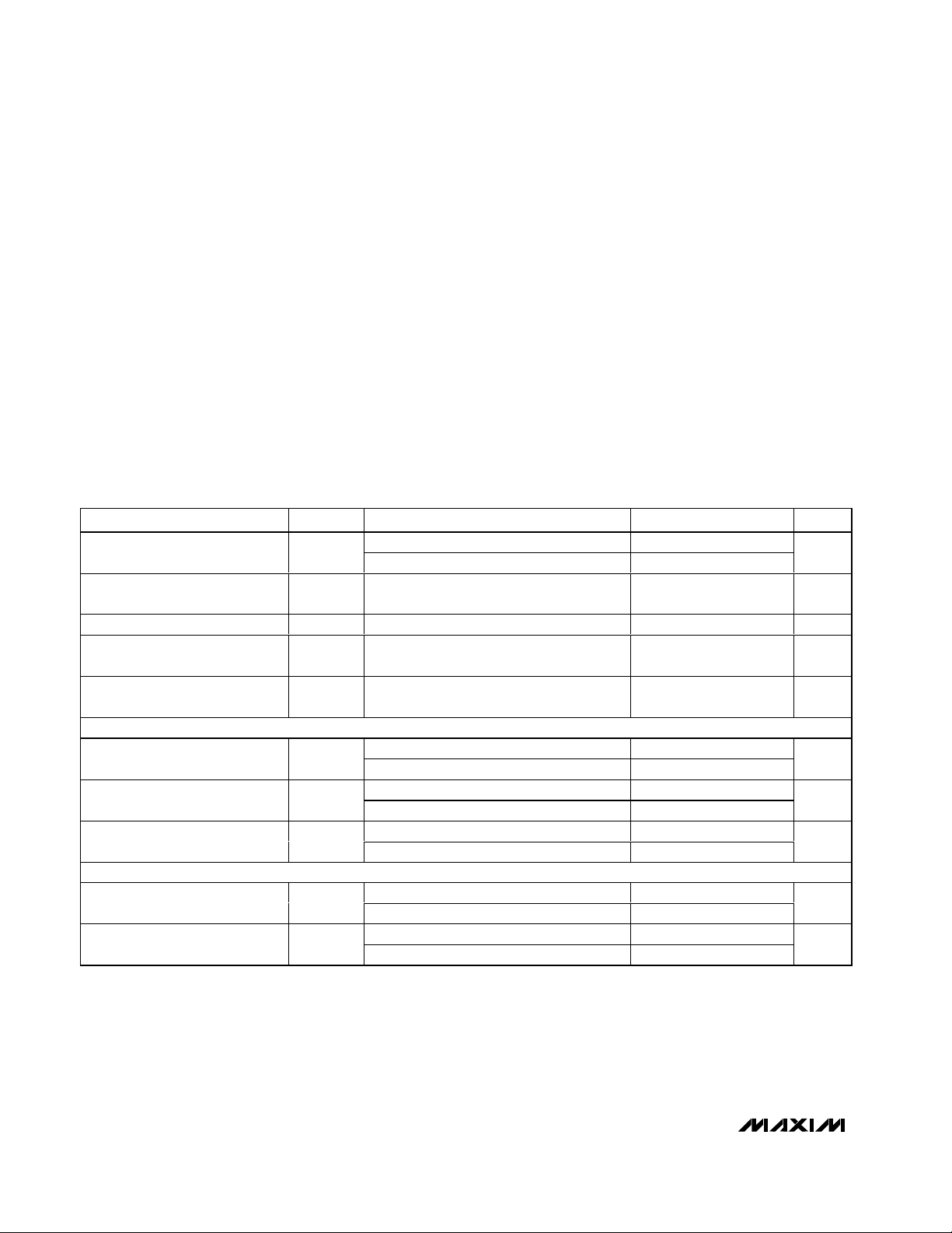
Typical Operating Characteristics
(VIN= VL= VCC= 5V, typical values are at TA = +25°C, unless otherwise noted.)
EFFICIENCY vs. LOAD CURRENT
MAX8545/46/48 toc01
LOAD CURRENT (A)
(CIRCUIT OF FIGURE 1; TABLE 1a)
EFFICIENCY (%)
10.1
10
20
30
40
50
60
70
80
90
100
0
0.01 10
VIN = 3.3V
V
OUT
= 1.2V
EFFICIENCY vs. LOAD CURRENT
MAX8545/46/48 toc02
LOAD CURRENT (A)
(CIRCUIT OF FIGURE 1; TABLE 1a)
EFFICIENCY (%)
10.1
10
20
30
40
50
60
70
80
90
100
0
0.01 10
VIN = 5V
V
OUT
= 1.8V
V
OUT
= 3.3V
EFFICIENCY vs. LOAD CURRENT
MAX8545/46/48 toc03
LOAD CURRENT (A)
(CIRCUIT OF FIGURE 2; TABLE 2a)
EFFICIENCY (%)
10.1
10
20
30
40
50
60
70
80
90
100
0
0.01 10
V
OUT
= 1.8V
V
OUT
= 3.3V
VIN = 12V
EFFICIENCY vs. LOAD CURRENT
MAX8545/46/48 toc04
LOAD CURRENT (A)
(CIRCUIT OF FIGURE 2; TABLE 2a)
EFFICIENCY (%)
10.1
10
20
30
40
50
60
70
80
90
100
0
0.01 10
VIN = 17V
V
OUT
= 3.3V
V
OUT
= 1.8V
EFFICIENCY vs. LOAD CURRENT
MAX8545/46/48 toc05
LOAD CURRENT (A)
EFFICIENCY (%)
10.1
10
20
30
40
50
60
70
80
90
100
0
0.01 10
V
OUT
= 1.8V
V
OUT
= 1.2V
VIN = 3.3V
(CIRCUIT OF FIGURE 1; TABLE 1b)
EFFICIENCY vs. LOAD CURRENT
MAX8545/46/48 toc06
LOAD CURRENT (A)
EFFICIENCY (%)
10.1
10
20
30
40
50
60
70
80
90
100
0
0.01 10
V
OUT
= 3.3V
V
OUT
= 2.5V
V
OUT
= 1.8V
V
OUT
= 1.2V
VIN = 5V
(CIRCUIT OF FIGURE 1; TABLE 1b)
EFFICIENCY vs. LOAD CURRENT
MAX8545/46/48 toc07
LOAD CURRENT (A)
EFFICIENCY (%)
10.1
10
20
30
40
50
60
70
80
90
100
0
0.01 10
V
OUT
= 3.3V
V
OUT
= 2.5V
V
OUT
= 1.8V
V
OUT
= 1.2V
VIN = 12V
(CIRCUIT OF FIGURE 2; TABLE 2b)
EFFICIENCY vs. LOAD CURRENT
MAX8545/46/48 toc08
LOAD CURRENT (A)
EFFICIENCY (%)
10.1
10
20
30
40
50
60
70
80
90
100
0
0.01 10
V
OUT
= 3.3V
V
OUT
= 2.5V
V
OUT
= 1.8V
V
OUT
= 1.2V
VIN = 17V
(CIRCUIT OF FIGURE 2; TABLE 2b)
CHANGE IN OUTPUT VOLTAGE
vs. LOAD CURRENT
MAX8545/46/48 toc09
LOAD CURRENT (A)
OUTPUT VOLTAGE (V)
5432
2.485
2.490
2.495
2.500
2.505
2.510
2.515
2.520
2.480
16
V
OUT
= 2.5V
V
IN
= 12V
Page 5
MAX8545/MAX8546/MAX8548
Low-Cost, Wide Input Range, Step-Down
Controllers with Foldback Current Limit
_______________________________________________________________________________________ 5
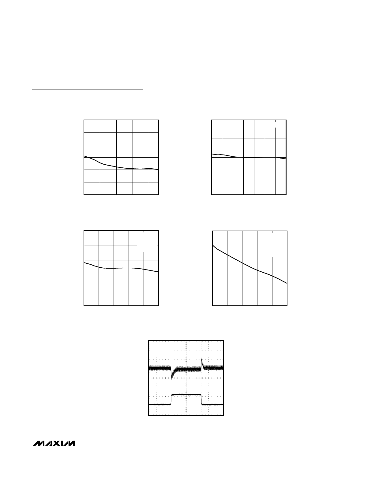
Typical Operating Characteristics (continued)
(VIN= VL= VCC= 5V, typical values are at TA = +25°C, unless otherwise noted.)
1.84
1.83
1.82
1.81
1.80
OUTPUT VOLTAGE (V)
1.79
1.78
CHANGE IN OUTPUT VOLTAGE
vs. INPUT VOLTAGE
2.5
INPUT VOLTAGE (V)
FREQUENCY vs. INPUT VOLTAGE
310
306
302
I
= 6V
LOAD
4.54.03.53.0
V
= 2.5V
OUT
NO LOAD
MAX8545/
MAX8546
MAX8545/46/48 toc10
MAX8545/46/48 toc12
2.52
2.51
2.50
OUTPUT VOLTAGE (V)
2.49
2.48
10
310
306
302
CHANGE IN OUTPUT VOLTAGE
vs. INPUT VOLTAGE
I
= 6V
LOAD
18 20 22 24161412
INPUT VOLTAGE (V)
FREQUENCY vs. TEMPERATURE
VIN = 12V
= 2.5V
V
OUT
NO LOAD
MAX8545/
MAX8546
MAX8545/46/48 toc11
MAX8545/46/48 toc13
298
FREQUENCY (kHz)
294
290
2.70 28.00
INPUT VOLTAGE (V)
22.9417.8812.827.76
LOAD TRANSIENT RESPONSE
VIN = 17V
= 2.5V
V
OUT
0
40µs/div
298
FREQUENCY (kHz)
294
290
-40.00 85.00
TEMPERATURE (°C)
MAX8545 toc14
V
OUT
AC COUPLED
100mV/div
I
OUT
5A/div
60.0035.0010.00-15.00
Page 6
MAX8545/MAX8546/MAX8548
Low-Cost, Wide Input Range, Step-Down
Controllers with Foldback Current Limit
6 _______________________________________________________________________________________
Typical Operating Characteristics (continued)
(VIN= VL= VCC= 5V, typical values are at TA = +25°C, unless otherwise noted.)
V
OUT
1V/div
V
IN
5V/div
INDUCTOR
CURRENT
5A/div
1ms/div
START-UP WAVEFORM
MAX8545 toc15
I
LOAD
= 3A
V
OUT
1V/div
V
IN
5V/div
INDUCTOR
CURRENT
2A/div
2ms/div
SHUTDOWN WAVEFORM
MAX8545 toc16
I
LOAD
= 3A
V
OUT
2V/div
V
IN
5V/div
I
IN
10A/div
I
OUT
5A/div
SHORT-CIRCUIT WAVEFORM
MAX8545 toc18
V
OUT
2V/div
V
IN
20V/div
I
IN
2A/div
INDUCTOR
CURRENT
5A/div
1ms/div
0
0
0
0
SHORT-CIRCUIT WAVEFORM
MAX8545 toc17
GAIN AND PHASE vs. FREQUENCY
MAX8545/46/48 toc19
FREQUENCY (kHz)
GAIN (dB)
PHASE (DEGREES)
101
-120
-100
-80
-60
-40
-20
0
20
40
60
-140
0.1 100
180
150
120
90
60
30
VIN = 17V, V
OUT
= 2.5V
I
LOAD
= 6A
GAIN
PHASE
Page 7

MAX8545/MAX8546/MAX8548
Low-Cost, Wide Input Range, Step-Down
Controllers with Foldback Current Limit
_______________________________________________________________________________________ 7
Pin Description
Functional Diagram
PIN NAME FUNCTION
1 COMP/EN
Compensation Input. Pull COMP/EN low with an open-collector or open-drain device to turn
off the output.
2 FB Feedback Input. Connect a resistive-divider network to set V
3V
4V
CC
IN
5VL
Internal Chip Supply. Connect VCC to VL through a 10Ω resistor. Bypass VCC to GND with at
least a 0.1µF ceramic capacitor.
Power Supply for LDO Regulator for VIN > 5.5V, and Chip Supply for VIN < 5.5V. Bypass VIN with
at least a 1µF ceramic capacitor to GND.
Output of Internal 5V LDO. Connect VL to V
for VIN < 5.5V. Bypass VL with at least a 1µF ceramic
IN
capacitor to GND.
. FB threshold is 0.8V.
OUT
6 DL Low-Side External MOSFET Gate-Driver Output. DL swings from VL to GND.
7 GND Ground and Negative Current-Sense Input
8 LX Inductor Switching Node. LX is used for both current limit and the return supply of the DH driver.
9 DH High-Side External MOSFET Gate-Driver Output. DH swings from BST to LX.
10 BST Positive Supply of DH Driver. Connect a 0.1µF ceramic capacitor between BST and LX.
V
VL
COMP/EN
FB
V
IN
CC
5V LINEAR
REGULATOR
RAMP
GENERATOR
INTERNAL
CHIP SUPPLY
800mV
SOFT-START
REF
100kHz/
300kHz*
CLOCK
GENERATOR
*SEE SELECTOR GUIDE
1V
ERROR
AMPLIFIER
PWM COMP
TEMPERATURE
SHUTDOWN
CONTROL
LOGIC
MAX8545
MAX8546
MAX8548
CURRENT-LIMIT
COMPARATOR
BST
DH
LX
DL
GND
FOLD-
FB
BACK
Page 8

MAX8545/MAX8546/MAX8548
Low-Cost, Wide Input Range, Step-Down
Controllers with Foldback Current Limit
8 _______________________________________________________________________________________
Detailed Description
The MAX8545/MAX8546/MAX8548 are BiCMOS switchmode power-supply controllers designed to implement
simple, buck-topology regulators in cost-sensitive
applications. The main power-switching circuit consists
of two N-channel MOSFETs, an inductor, and input/output filter capacitors. An all N-channel synchronous-rectified design provides high efficiency at reduced cost.
These devices have an internal 5V linear regulator that
steps down the input voltage to supply the IC and the
gate drivers. The low-side-switch gate driver is directly
powered from the 5V regulator (VL), while the highside-switch gate driver is indirectly powered from VL
plus an external diode-capacitor boost circuit.
Current-Limit and
Short-Circuit Protection
The MAX8545/MAX8546/MAX8548 employ a valley current-sensing algorithm that uses the R
DS(ON)
of the lowside N-channel MOSFET to sense the current. This
eliminates the need for an external sense resistor usually
placed in series with the output. The voltage measured
across the low-side MOSFET’s R
DS(ON)
is compared to
a fixed -320mV reference for the MAX8545/MAX8548
and a fixed -165mV reference for the MAX8546. The current limit is given by the equations below:
Aside from current limiting, these devices feature foldback short-circuit protection. This feature is designed
to reduce the current limit by 80% as the output voltage
drops to 0V.
MOSFET Gate Drivers
The DH and DL drivers are optimized for driving Nchannel MOSFETs with low gate charge. An adaptive
dead-time circuit monitors the DL output and prevents
the high-side MOSFET from turning on until the low-side
MOSFET is fully off. There must be a low-resistance,
low-inductance connection from the DL driver to the
MOSFET gate for the adaptive dead-time circuit to work
properly. Otherwise, the sense circuitry in the MAX8545/
MAX8546/MAX8548 may detect the MOSFET gate as off
while there is actually charge left on the gate. Use very
short, wide traces measuring no less than 50 to 100 mils
wide if the MOSFET is 1 inch away from the MAX8545/
MAX8546/MAX8548. The same type of adaptive deadtime circuit monitors the DH off edge. The same recommendations apply for the gate connection of the
high-side MOSFET.
The internal pulldown transistor that drives DL low is
robust, with a 1.1Ω (typ) on-resistance. This helps prevent DL from being pulled up due to capacitive coupling from the drain to the gate of the low-side
synchronous-rectifier MOSFET during the fast rise time
of the LX node.
Soft-Start
The MAX8545/MAX8546/MAX8548 feature an internally
set soft-start function that limits inrush current. It accomplishes this by ramping the internal reference input to the
controller’s transconductance error amplifier from 0 to
the 0.8V reference voltage. The ramp time is 1024 oscillator cycles for the MAX8548 and 2048 oscillator cycles
for the MAX8545/MAX8546. At the nominal 100kHz and
300kHz switching rate, the soft-start ramp is approximately 10.2ms and 6.8ms, respectively.
High-Side Gate-Drive Supply (BST)
A flying-capacitor boost circuit generates gate-drive voltage for the high-side N-channel MOSFET. The flying
capacitor is connected between the BST and LX nodes.
On startup, the synchronous rectifier (low-side MOSFET)
forces LX to ground and charges the boost capacitor to
VL. On the second half-cycle, the MAX8545/MAX8546/
MAX8548 turn on the high-side MOSFET by closing an
internal switch between BST and DH. This provides the
necessary gate-to-source voltage to drive the high-side
MOSFET gate above its source at the input voltage.
Internal 5V Linear Regulator
All MAX8545/MAX8546/MAX8548 functions are internally
powered from an on-chip, low-dropout 5V regulator (VL).
These devices have a maximum input voltage (VIN) of
28V. Connect VCCto VLthrough a 10Ω resistor and
bypass VCCto GND with a 0.1µF ceramic capacitor. The
VIN-to-VL dropout voltage is typically 140mV, so when V
IN
is less than 5.5V, VL is typically VIN- 140mV.
The internal linear regulator can source a minimum of
25mA and a maximum of approximately 40mA to supply
power to the IC low-side and high-side MOSFET drivers.
Duty-Cycle Limitations for
Low V
OUT/VIN
Ratios
The MAX8545/MAX8546/MAX8548’s output voltage is
adjustable down to 0.8V. However, the minimum duty
cycle can limit the ability to supply low-voltage outputs
I
LIMIT
=
320
R
DS ON
mV
(/)
MAX MAX
()
8545 8548
mV
=
165
R
DS ON
8546
()
MAX
()
I
LIMIT
Page 9
MAX8545/MAX8546/MAX8548
Low-Cost, Wide Input Range, Step-Down
Controllers with Foldback Current Limit
_______________________________________________________________________________________ 9
from high-voltage inputs. With high input voltages, the
required duty factor is approximately:
where R
DS(ON)
x I
LOAD
is the voltage drop across the
synchronous rectifier. Therefore, the maximum input
voltage (V
IN(DFMAX)
) that can supply a given output
voltage is:
If the circuit cannot attain the required duty cycle dictated by the input and output voltages, the output voltage still remains in regulation. However, there may be
intermittent or continuous half-frequency operation as
the controller attempts to lower the average duty cycle
by deleting pulses. This can increase output voltage
ripple and inductor current ripple, which increases
noise and reduces efficiency. Furthermore, circuit stability is not guaranteed.
Applications Information
Design Procedures
1) Input Voltage Range. The maximum value
(V
IN(MAX)
) must accommodate the worst-case high
input voltage. The minimum value (V
IN(MIN)
) must
account for the lowest input voltage after drops due
to connectors, fuses, and switches are considered.
In general, lower input voltages provide the best
efficiency.
2) Maximum Load Current. There are two current
values to consider. Peak load current (I
LOAD(MAX)
)
determines the instantaneous component stresses
and filtering requirements and is key in determining
output capacitor requirements. I
LOAD(MAX)
also
determines the required inductor saturation rating.
Continuous load current (I
LOAD
) determines the
thermal stresses, input capacitor, and MOSFETs,
as well as the RMS ratings of other heat-contributing components such as the inductor.
3) Inductor Value. This choice provides tradeoffs
between size, transient response, and efficiency.
Higher inductance value results in lower inductor
ripple current, lower peak current, lower switching
losses, and, therefore, higher efficiency at the cost
of slower transient response and larger size. Lower
inductance values result in large ripple currents,
smaller size, and poor efficiency, while also providing faster transient response.
Setting the Output Voltage
An output voltage between 0.8V and (0.83 x VIN) can
be configured by connecting FB to a resistive divider
between the output and GND (see Figures 1 and 2).
Select resistor R4 in the 1kΩ to 10kΩ range. R3 is then
given by:
where VFB= +0.8V.
Inductor Selection
Determine an appropriate inductor value with the following equation:
where LIR is the ratio of inductor ripple current to average continuous maximum load current. Choosing LIR
between 20% to 40% results in a good compromise
between efficiency and economy. Choose a low-coreloss inductor with the lowest possible DC resistance.
Ferrite-core-type inductors are often the best choice for
performance; however, the MAX8548’s low switching
frequency also allows the use of powdered iron core
inductors in ultra-low-cost applications where efficiency
is not critical. With any core material, the core must be
large enough not to saturate at the peak inductor current (I
PEAK
).
Setting the Current Limit
The MAX8545/MAX8546/MAX8548 provide valley current limit by sensing the voltage across the external
low-side MOSFET. The minimum current-limit threshold
voltage is -280mV for the MAX8545/MAX8548 and
-140mV for the MAX8546. The MOSFET on-resistance
required to allow a given peak inductor current is:
where I
VALLEY
= I
LOAD(MAX)
x (1 - LIR / 2), and
R
DS(ON)MAX
is the maximum on-resistance of the lowside MOSFET at the maximum operating junction
temperature.
)
V
IN DFMAX
VR I
+×()
OUT DS ON LOAD
1
≤+×
DC
()
V
IN
VR I
()
MIN
()
OUT DS ON LOAD() ()
RR
V
34
OUT
V
FB
1=−
LV
=×
OUT
V f LIR I
IN OSC LOAD MAX
R
DS ON MAX
R
DS ON MAX
II
=+
PEAK LOAD MAX LOAD MAX
.
028
()
()
≤
I
VALLEY
.
014
I
VALLEY
VV
−
()
IN OUT
×××
LIR
() ()
2
×
()
I
V
( /
for the MAX MAX
V
( )≤
for the MAX
8545 8548
8546
Page 10

MAX8545/MAX8546/MAX8548
Low-Cost, Wide Input Range, Step-Down
Controllers with Foldback Current Limit
10 ______________________________________________________________________________________
Figure 1. Typical Application Circuit (2.7V to 5V) Input (see Tables 1a, 1b)
Figure 2. Typical Application Circuit (10V to 24V) Input (see Tables 2a, 2b)
+2.7V TO
+5.5V INPUT
C3 C2C4
R1
C9
IN
CC
MAX8545*
MAX8546
MAX8548*
COMP/
EN
D2 R2
C10 C11
*FOLLOW THE DATA SHEET DESIGN PROCEDURE TO SELECT THE
EXTERNAL COMPONENTS FOR THE MAX8545/MAX8548.
C1
VLV
BSTV
DH
LX
DL
GND
FB
D1
Q1
C5
R3
R4
L1
C6
C7 C8
OUT
1.8V/3A OR 6A
+10V TO
D2 R2
*FOLLOW THE DATA SHEET DESIGN PROCEDURE TO SELECT THE
EXTERNAL COMPONENTS FOR THE MAX8545/MAX8548.
+24V INPUT
C12
C10 C11
R1
C9
CC
V
IN
MAX8545*
MAX8546
MAX8548*
COMP/
EN
C1
VLV
BST
DH
LX
DL
GND
FB
D1
C5
R4
C3 C2C4
Q1
L1
C6
C7 C8
R3
OUT
2.5V/3A OR 6A
Page 11

MAX8545/MAX8546/MAX8548
Low-Cost, Wide Input Range, Step-Down
Controllers with Foldback Current Limit
______________________________________________________________________________________ 11
A limitation of sensing current across a MOSFET’s onresistance is that the current-limit threshold is not accurate since MOSFET R
DS(ON)
specifications are not
precise. This type of current limit provides a coarse level
of fault protection. It is especially suited when the input
source is already current-limited or otherwise protected.
Power MOSFET Selection
The MAX8545/MAX8546/MAX8548 drive two external,
logic-level, N-channel MOSFETs as the circuit switching elements. The key selection parameters are:
1) On-resistance (R
DS(ON)
): the lower, the better.
2) Maximum drain-to-source voltage (V
DSS
) should be
at least 10% higher than the input supply rail at the
high-side MOSFET’s drain.
3) Gate charges (Qg, Qgd, Qgs): the lower, the better.
Choose the MOSFETs with rated R
DS(ON)
at VGS= 4.5V
for an input voltage greater than 5V, and at VGS= 2.5V
for an input voltage less than 5.5V. For a good compromise between efficiency and cost, choose the high-side
MOSFET (N1) that has conduction losses equal to the
switching losses at nominal input voltage and maximum
output current. For N2, make sure it does not spuriously
turn on due to a dV/dt caused by N1 turning on as this
would result in shoot-through current degrading the
efficiency. MOSFETs with a lower Qgd/ Qgsratio have
higher immunity to dV/dt.
MOSFET Power Dissipation
For proper thermal-management design, the power dissipation must be calculated at the desired maximum
operating junction temperature, maximum output current, and worst-case input voltage (for the low-side
MOSFET (N2) the worst case is at V
IN(MAX)
, for the highside MOSFET (N1) the worst case can be either at
V
IN(MIN)
or V
IN(MAX)
). N1 and N2 have different loss
components due to the circuit operation. N2 operates as
a zero-voltage switch; therefore, the major losses are:
the channel conduction loss (P
N2CC
), the body-diode
conduction loss (P
N2DC
), and the gate-drive loss
(P
N2DR
).
Use R
DS(ON)
at T
J(MAX)
.
where V
F
is the body-diode forward voltage drop, tdtis
the dead time between N1 and N2 switching transitions
(which is 30ns), and fSis the switching frequency.
Because of zero-voltage switch operation, the N2 gatedrive losses are due to charging and discharging the
input capacitor, C
ISS
. These losses are distributed
between the average DL gate driver’s pullup and pulldown resistors and the internal gate resistance. The
RDLis typically 1.8Ω, and the internal gate resistance
(R
GATE
) of the MOSFET is typically 2Ω. The drive
power dissipated in N2 is given by:
N1 operates as a duty-cycle control switch and has the
following major losses: the channel conduction loss
(P
N1CC
), the voltage and current overlapping switching
loss (P
N1SW
), and the drive loss (P
N1DR
). N1 does not
have a body-diode conduction loss because the diode
never conducts current.
Use R
DS(ON)
at T
J(MAX)
.
where I
GATE
is the average DH high driver output-cur-
rent capability determined by:
where RDHis the high-side MOSFET driver’s average
on-resistance (2.05Ω typ) and R
GATE
is the internal
gate resistance of the MOSFET (2Ω typ).
where VGS~ VL.
In addition to the losses above, allow about 20% more
for additional losses due to MOSFET output capacitance and N2 body-diode reverse recovery charge dissipated in N1. Refer to the MOSFET data sheet for
thermal resistance specifications to calculate the PC
board area needed. This information is essential to
maintain the desired maximum operating junction temperature with the above calculated power dissipation.
To reduce EMI caused by switching noise, add a 0.1µF
ceramic capacitor from the high-side MOSFET drain to
the low-side MOSFET source or add resistors in series
P
NCC
1=−
PIVtf
N DC LOAD F dt S2
V
OUT
××
V
IN
2=× × × ×
2
IR
LOAD
DS ON2
()
PCVf
=×
N DR ISS GS S
2
2
()
××
R
GATE
RR
+
GATE DL
P
NCC
PVI f
=
=× ××
N SW IN LOAD S
1
V
OUT
V
IN
×
()
2
IR
LOAD DS ON1
×
QQ
GS GD
I
GATE
()
+
I
GATE ON
()
1
=×
2
VL
+
RR
DH GATE
PQVf
=×××
NDR GS GS S
1
R
GATE
+
RR
DH GATE
Page 12

MAX8545/MAX8546/MAX8548
Low-Cost, Wide Input Range, Step-Down
Controllers with Foldback Current Limit
12 ______________________________________________________________________________________
with DH and DL to slow down the switching transitions.
However, adding series resistors increases the power
dissipation of the MOSFET, so ensure temperature ratings of the MOSFET are not exceeded.
Input-Capacitor Selection
The input capacitors (C2 and C3 in Figure 1) reduce
noise injection and current peaks drawn from the input
supply. The input capacitor must meet the ripple-current requirement (I
RMS
) imposed by the switching cur-
rents. The RMS input ripple current is given by:
For optimal circuit reliability, choose a capacitor that
has less than 10°C temperature rise at the RMS current.
I
RMS
is maximum when the input voltage equals 2 x
V
OUT
, where I
RMS
= 1/2 I
LOAD
.
Output Capacitor Selection
The key parameters for the output capacitor are the
actual capacitance value, the equivalent series resistance (ESR), the equivalent series inductance (ESL),
and the voltage-rating requirements. All these parameters affect the overall stability, output ripple voltage,
and transient response.
The output ripple has three components: variations in the
charge stored in the output capacitor, the voltage drop
across the ESR, and the voltage drop across the ESL.
V
RIPPLE
= V
RIPPLE(ESR)
+ V
RIPPLE(C)
+ V
RIPPLE(ESL)
The output voltage ripple as a consequence of the ESR
and output capacitance is:
where I
P-P
is the peak-to-peak inductor current (see the
Inductor Selection section).
While these equations are suitable for initial capacitor
selection to meet the ripple requirement, final values
may also depend on the relationship between the LC
double-pole frequency and the capacitor ESR-zero frequency. Generally, the ESR zero is higher than the LC
double pole; however, it is preferable to keep the ESR
zero close to the LC double pole when possible to
negate the sharp phase shift of the typically high-Q
double LC pole (see the Compensation Design section). Aluminum electrolytic or POS capacitors are recommended. Higher output current requires multiple
capacitors to meet the output ripple voltage.
The MAX8545/MAX8546/MAX8548s’ response to a load
transient depends on the selected output capacitor. After
a load transient, the output instantly changes by (ESR x
∆I
LOAD
) + (ESL x dI/dt). Before the controller can
respond, the output deviates further depending on the
inductor and output capacitor values. After a short period
of time (see the Typical Operating Characteristics), the
controller responds by regulating the output voltage back
to its nominal state. The controller response time
depends on the closed-loop bandwidth. Higher bandwidth results in faster response time, preventing the output voltage from further deviation. Do not exceed the
capacitor’s voltage or ripple-current ratings.
Boost Diode and Capacitor Selection
A low-current Schottky diode, such as the CMPSH-3
from Central Semiconductor, works well for most applications. Do not use large power diodes since higher
junction capacitance can charge up BST to LX voltage
that could exceed the device rating of 6V. The boost
capacitor should be in the range of 0.1µF to 0.47µF,
depending on the specific input and output voltages
and the external components and PC board layout. The
boost capacitance needs to be as large as possible to
prevent it from charging to excessive voltage, but small
enough to adequately charge during the minimum lowside MOSFET conduction time, which happens at the
maximum operating duty cycle (this occurs at the minimum input voltage). In addition, ensure the boost
capacitor does not discharge to below the minimum
gate-to-source voltage required to keep the high-side
MOSFET fully enhanced for lowest on-resistance. This
minimum gate-to-source voltage V
GS(MIN)
is deter-
mined by:
where Qg is the total gate charge of the high-side
MOSFET and C
BOOST
is the boost capacitor value.
Compensation Design
The MAX8545/MAX8546/MAX8548 use a voltage-mode
control scheme that regulates the output voltage. This is
done by comparing the error amplifier’s output (COMP) to
a fixed internal ramp. The inductor and output capacitor
create a double pole at the resonant frequency, which
VVV
×−
()
II
=×
RMS LOAD
OUT IN OUT
V
IN
V I ESR
RIPPLE ESR P P
V
RIPPLE C
V
RIPPLE ESL
=
I
PP
−
=×
()
()
()
VV
IN OUTSWOUT
−
I
=
−
fLVV
PP
××
8
Cf
OUT SW
×
V ESL
IN
=
+
L ESL
×
−
IN
Q
VV
GS MIN L
=−
()
C
BOOST
G
Page 13

MAX8545/MAX8546/MAX8548
Low-Cost, Wide Input Range, Step-Down
Controllers with Foldback Current Limit
______________________________________________________________________________________ 13
has a gain drop of 40dB per decade, and a phase shift
of 180°. The error amplifier must compensate for this
gain drop and phase shift to achieve a stable highbandwidth, closed-loop system.
The basic regulator loop consists of a power modulator
(Figure 3), an output feedback divider, and an error
amplifier. The power modulator has DC gain set by
VIN/V
RAMP
, with a double pole set by the inductor and
output capacitor, and a single zero set by the output
capacitor (C
OUT
) and its equivalent series resistance
(ESR). Below are equations that define the power modulator:
The DC gain of the power modulator is:
where V
RAMP
= 1V.
The pole frequency due to the inductor and output
capacitor is:
The zero frequency due to the output capacitor’s ESR is:
The output capacitor is usually comprised of several
same capacitors connected in parallel. With n capacitors in parallel, the output capacitance is:
C
OUT
= n X C
EACH
The total ESR is:
The ESR zero (f
ZESR
) for a parallel combination of
capacitors is the same as for an individual capacitor.
The feedback divider has a gain of GFB= VFB/V
OUT
,
where VFBis 0.8V.
The transconductance error amplifier has DC gain
G
EA(dc)
of 72dB. A dominant pole (f
DPEA
) is set by the
compensation capacitor (CC), the amplifier output
resistance (RO) equals 37MΩ, and the compensation
resistor (RC):
The compensation resistor and the compensation
capacitor set a zero:
The total closed-loop gain must equal unity at the
crossover frequency. The crossover frequency should
be higher than f
ZESR
, so that the -1 slope is used to
cross over at unity gain. Also, the crossover frequency
should be less than or equal to 1/5 the switching frequency (fSW) of the controller.
The loop-gain equation at the crossover frequency is:
VFB/V
OUT
x G
EA(fC)
x G
MOD(fC)
= 1
where G
EA(fc)
= g
mEA
× RC, and G
MOD(fc)
= G
MOD(DC)
× (f
PMOD
)2 / (f
ZESR
× fC).
The compensation resistor, RC, is calculated from:
RC= V
OUT
/ g
mEA
x VFBx G
MOD(fC)
where g
mEA
= 108µS.
Due to the underdamped (Q > 1) nature of the output
LC double pole, the error-amplifier compensation zero
should be approximately 0.2 f
PMOD
to provide good
phase boost. CCis calculated from:
A small capacitor, CF, can also be added from COMP to
GND to provide high-frequency decoupling. CFadds
another high-frequency pole, f
PHF
, to the error-amplifier
response. This pole should be greater than 100 times the
error-amplifier zero frequency to have negligible impact
on the phase margin. This pole should also be less than
1/2 the switching frequency for effective decoupling.
100 f
ZEA
< f
PHF
< 0.5 f
sw
Select a value for f
PHF
in the range given above, then
solve for CFusing the following equation:
PC Board Layout Guidelines
Careful PC board layout is critical to achieve low switching losses and stable operation. If possible, mount all the
power components on the top side of the board with their
G
MOD DC
()
=
V
IN
V
RAMP
f
PMOD
f
ZESR
=
=
LC
2π
××
2π
1
OUT
1
ESR C
OUT
ESR
=
ESR
EACH
n
f
DPEA
=
2π
1
CRR
×× +
()
COC
f
ZEA
=
CR
××
2π
1
CC
ff
ZESR C
<≤
f
SW
5
C
=
C
2π
5
Rf
××
CPMOD
C
F
=
××
2π
1
Rf
C PHF
Page 14

MAX8545/MAX8546/MAX8548
Low-Cost, Wide Input Range, Step-Down
Controllers with Foldback Current Limit
14 ______________________________________________________________________________________
ground terminals flush against one another. Follow these
guidelines for good PC board layout:
1) Keep the high-current paths short, especially at the
ground terminals. This practice is essential for stable, jitter-free operation.
2) Connect the power and analog grounds close to
the IC pin 7.
3) Keep the power traces and load connections short.
This practice is essential for high efficiency. Using
thick copper PC boards (2oz vs. 1oz) can enhance
full-load efficiency by 1% or more. Correctly routing
PC board traces is a difficult task that must be
approached in terms of fractions of centimeters,
where a few milohms of excess trace resistance
cause a measurable efficiency penalty.
4) LX and GND connections to the low-side MOSFET
for current sensing must be made using Kelvin
sense connections to guarantee the current-limit
accuracy. With SO-8 MOSFETs, this is best done
by routing power to the MOSFETs from outside
using the top copper layer, while connecting LX
and GND inside (underneath) the SO-8 package.
5) When tradeoffs in trace lengths must be made, it’s
preferable to allow the inductor charging current
path to be longer than the discharge path. For
example, it’s better to allow some extra distance
between the inductor and the low-side MOSFET or
between the inductor and the output filter capacitor.
6) Ensure that the connection between the inductor
and C3 is short and direct.
7) Route switching nodes (BST, LX, DH, and DL) away
from sensitive analog areas (COMP and FB).
Ensure the C1 ceramic bypass capacitor is immediately
adjacent to the pins and as close to the device as possible. Furthermore, the VINand GND pins of MAX8545/
MAX8546/MAX8548 must terminate at the two ends of
C1 before connecting to the power switches and C2.
Figure 3. Compensation Scheme
V
IN
RAMP
GENERATOR
PWM
COMP/EN
R2
C10
MAX8545
MAX8546
MAX8548
ERROR
AMPLIFIER
0.8V
DH
LX
DL
FB
N
L
N
V
OUT
C
OUT
R3
R4
Page 15

MAX8545/MAX8546/MAX8548
Low-Cost, Wide Input Range, Step-Down
Controllers with Foldback Current Limit
______________________________________________________________________________________ 15
Table 1a. Component Selection for
Standard Applications for VIN= 2.7V to
5.5V, V
OUT
= 1.8V / 3A (Figure 1)
(MAX8546 Only)
Table 1b. Component Selection for
Standard Applications for V
IN
= 2.7V to
5.5V, V
OUT
= 1.8V / 6A (Figure 1)
(MAX8546 Only)
COMPONENT QTY DESCRIPTION
C1, C4 2
C2 0 Not installed
C3 1
C5, C8, C9 3
C6, C7 2
C10 1
C11 0 Not installed
D1, D2 2
L1 1
Q1 1
R1 1 10Ω ±5% resistor
R2 1 150kΩ ±5% resistor
R3 1 5.11kΩ ±1% resistor
R4 1 4.02kΩ ±1% resistor
1µF, 10V X7R ceramic capacitors
Taiyo Yuden LMK212BJ105MG
1200µF, 10V, 44mΩ, 1.25A aluminum
electrolytic capacitor
Sanyo 10MV1200AX
(10 x 16 case size)
0.1µF, 10V X7R ceramic capacitors
Kemet C0603C104M8RAC
1000µF, 6.3V, 69mΩ, 0.8A aluminum
electrolytic capacitors
Sanyo 6.3MV1000AX (8 x 20 case size)
1.5nF, 10V X7R ceramic capacitor
Kemet C0603C152M8RAC
30V, 100mA Schottky diodes
Central Semiconductor CMPSH-3
4.7µH, 5.7A, 18mΩ inductor
Sumida CDRH124-4R7
20V/30V, 35mΩ dual N-channel
8-pin SO
V i shay S i 4966D Y ( f o r 2.7 V t o 3.6 V
Fair chil d FD S 6912A ( f or 4 .5 V t o 5 .5 V
IN
)
IN
COMPONENT QTY DESCRIPTION
C1, C4 2
C2, C3 2
C5, C8, C9 3
C6, C7 2
C10 1
C11 0 Not installed
D1, D2 2
L1 1
Q1 1
R1 1 10Ω ±5% resistor
)
R2 1 110kΩ ±5% resistor
R3 1 5.11kΩ ±1% resistor
R4 1 4.02kΩ ±1% resistor
1µF, 10V X7R ceramic capacitors
Taiyo Yuden LMK212BJ105MG
1200µF, 10V, 44mΩ, 1.25A aluminum
electrolytic capacitors
Sanyo 10MV1200AX
(10 x 16 case size)
0.1µF, 10V X7R ceramic capacitors
Kemet C0603C104M8RAC
1500µF, 6.3V, 44m Ω, 1.25A al um i num
el ectr ol ytic cap acitor s
S anyo 6.3M V1500AX (10 x 20 case si ze)
1.5nF, 10V X7R ceramic capacitor
Kemet C0603C152M8RAC
30V, 100mA Schottky diodes
Central Semiconductor CMPSH-3
2.1µH, 8A, 11.6mΩ inductor
Sumida CEP122-2R1
20V, 18m Ω d ual N- channel 8- pi n SO
Fair chil d FD S 6898A ( f or 2 .7 V t o 3 .6 V
Fair chil d FD S 6890A ( f or 4 .5 V t o 5 .5 V
IN
IN
)
)
Page 16
MAX8545/MAX8546/MAX8548
Low-Cost, Wide Input Range, Step-Down
Controllers with Foldback Current Limit
16 ______________________________________________________________________________________
Table 2a. Component Selection for
Standard Applications for VIN= 10V to
24V, V
OUT
= 2.5V / 3A (Figure 2)
(MAX8546 Only)
Table 2b. Component Selection for
Standard Applications for V
IN
= 10V to
24V, V
OUT
= 2.5V / 6A (Figure 2)
(MAX8546 Only)
COMPONENT QTY DESCRIPTION
C1 1
C2 0 Not installed
C3 1
C4, C12 2
C5, C8, C9 3
C6, C7 2
C10 1
C11 0 Not installed
D1, D2 2
L1 1
Q1 1
R1 1 10Ω ±5% resistor
R2 1 82kΩ ±5% resistor
R3 1 8.66kΩ ±1% resistor
R4 1 4.02kΩ ±1% resistor
1µF, 10V X7R ceramic capacitor
Taiyo Yuden LMK212BJ105MG
470µF, 35V, 39mΩ, 1.45A aluminum
electrolytic capacitor
Sanyo 35MV470AX
(10 x 22 case size)
1µF, 35V X7R ceramic capacitors
Taiyo Yuden GMK316BJ105ML
0.1µF, 10V X7R ceramic capacitors
Kemet C0603C104M8RAC
1000µF, 6.3V, 69mΩ, 0.8A aluminum
electrolytic capacitors
Sanyo 6.3MV1000AX
(8 x 20 case size)
6.8nF, 10V X7R ceramic capacitor
Kemet C0603C6822M8RAC
30V, 100mA Schottky diodes
Central Semiconductor CMPSH-3
8.2µH, 5.8A, 9.5mΩ inductor
Sumida CEP125-8R2
30V, 35mΩ dual N-channel 8-pin SO
Fairchild FDS6912A
COMPONENT QTY DESCRIPTION
C2, C3 2
C4, C12 2
C5, C8, C9 3
C6, C7 2
D1, D2 2
C1 1
C10 1
C11 0 Not installed
L1 1
Q1 1
R1 1 10Ω ±5% resistor
R2 1 68kΩ ±5% resistor
R3 1 8.66kΩ ±1% resistor
R4 1 4.02kΩ ±1% resistor
1µF, 10V X7R ceramic capacitor
Taiyo Yuden LMK212BJ105MG
470µF, 35V, 39mΩ, 1.45A aluminum
electrolytic capacitors
Sanyo 35MV470AX
(10 x 22 case size)
1µF, 35V X7R ceramic capacitors
Taiyo Yuden GMK316BJ105ML
0.1µF, 10V X7R ceramic capacitors
Kemet C0603C104M8RAC
1500µF, 6.3V, 44mΩ, 1.25A aluminum
electrolytic capacitors
Sanyo 6.3MV1500AX
(10 x 20 case size)
6.8nF, 10V X7R ceramic capacitor
Kemet C0603C682M8RAC
30V, 100mA Schottky diodes
Central Semiconductor CMPSH-3
4µH, 8.3A, 6.6mΩ inductor
Sumida CEP125-4R0
30V, 18mΩ (LSFET)/35mΩ (HSFET)
dual N-channel 8-pin SO
Fairchild FDS6982
Page 17

MAX8545/MAX8546/MAX8548
Low-Cost, Wide Input Range, Step-Down
Controllers with Foldback Current Limit
______________________________________________________________________________________ 17
Pin Configuration
Chip Information
TRANSISTOR COUNT: 3351
PROCESS: BiCMOS
TOP VIEW
COMP/EN
V
1
2
MAX8545
MAX8546
3
CC
IN
MAX8548
4
56
µMAX
109BST
DHFB
8
LX
7
GNDV
DLVL
Page 18

MAX8545/MAX8546/MAX8548
Low-Cost, Wide Input Range, Step-Down
Controllers with Foldback Current Limit
Maxim cannot assume responsibility for use of any circuitry other than circuitry entirely embodied in a Maxim product. No circuit patent licenses are
implied. Maxim reserves the right to change the circuitry and specifications without notice at any time.
18 ____________________Maxim Integrated Products, 120 San Gabriel Drive, Sunnyvale, CA 94086 408-737-7600
© 2003 Maxim Integrated Products Printed USA is a registered trademark of Maxim Integrated Products.
Package Information
(The package drawing(s) in this data sheet may not reflect the most current specifications. For the latest package outline information
go to www.maxim-ic.com/packages
.)
0.6±0.1
e
10
ÿ 0.50±0.1
1
0.6±0.1
TOP VIEW
D2
A2
b
D1
FRONT VIEW
4X S
10
H
1
BOTTOM VIEW
GAGE PLANE
A
A1
α
E2
E1
SIDE VIEW
INCHES
MAX
MIN
DIM
A1
A2 0.030 0.037 0.75 0.95
D1
D2
E1
E2
H
L
L1
b
e
c
S
α
c
L
L1
PROPRIETARY INFORMATION
TITLE:
0.043
-A
0.006
0.002
0.116
0.120
0.114
0.118
0.116
0.120
0.114
0.118
0.187
0.199
0.0157
0.0275
0.037 REF
0.007
0.0106
0.0197 BSC
0.0035
0.0078
0.0196 REF
6∞
0∞ 0∞ 6∞
PACKAGE OUTLINE, 10L uMAX/uSOP
21-0061
MILLIMETERS
MAX
MIN
1.10
-
0.15
0.05
3.05
2.95
3.00
2.89
3.05
2.95
2.89
3.00
4.75
5.05
0.40
0.70
0.940 REF
0.177
0.270
0.500 BSC
0.090
0.200
0.498 REF
10LUMAX.EPS
REV.DOCUMENT CONTROL NO.APPROVAL
1
I
1
 Loading...