

Page 1
General Description
The MAX8513/MAX8514 integrate a voltage-mode
PWM step-down DC-DC controller and two LDO controllers, a voltage monitor, and a power-on reset for the
lowest-cost power-supply and monitoring solution for
xDSL modems, routers, gateways, and set-top boxes.
The DC-DC controller switching frequency can be set
with an external resistor from 300kHz to 1.4MHz, to allow
for the optimization of cost, size, and efficiency. For noisesensitive applications, the DC-DC controller can also be
synchronized to an external clock, minimizing noise interference. Operation above 1.1MHz reduces noise for high
data-rate xDSL applications. An adjustable soft-start and
adjustable foldback current limit provide reliable startup
and fault protection. The DC-DC controller output voltage
can be set externally to a voltage from 1.25V to 5.5V.
Current limiting is accomplished by inductor current sensing for improved efficiency, or by an external sense resistor for better accuracy.
The MAX8513/MAX8514s’ first LDO controller is
designed to provide a low-cost, high-current regulated
output from 0.8V to 5.5V using an N-channel MOSFET or
a low-current output using a low-cost NPN transistor. The
MAX8513’s second regulator can be used to generate
0.8V to 27V output with a low-cost PNP transistor. Both
LDO regulators can operate either from the DC-DC controller output or from a higher voltage derived with a flyback overwinding on the DC-DC converter inductor. The
MAX8514’s second LDO regulator is designed to provide a negative output with an NPN transistor.
A sequence input allows the outputs to either power up
together, or for the DC-DC regulator to power up first
and each LDO controller to power up in sequence. An
input power-fail output (PFO) is provided for input
power-fail warning, such as in dying-gasp applications.
A power-on reset circuit with a 140ms delay is also
included to indicate when all outputs have achieved
regulation and stabilized.
Applications
xDSL, Cable, ISDN Modems, and Routers
Wireless Routers
Set-Top Boxes
Automotive Dashboard Electronics
Features
♦ Low-Cost DC-DC Controller with Two LDOs
♦ Wide Input Range: 4.5V to 28V
♦ 300kHz to 1.4MHz Adjustable Switching
Frequency
♦ Low Noise for High Data-Rate xDSL Applications
♦ Synchronizable to External Clock
♦ Adjustable Soft-Start
♦ Lossless Adjustable Foldback Current Limit
♦ Power-On Reset with 140ms Delay
♦ Adjustable Input Power-Fail Warning for Dying
Gasp
♦ Selectable Output-Voltage Sequencing or
Output-Voltage Tracking
MAX8513/MAX8514
Wide-Input, High-Frequency, Triple-Output Supplies
with Voltage Monitor and Power-On Reset
________________________________________________________________ Maxim Integrated Products 1
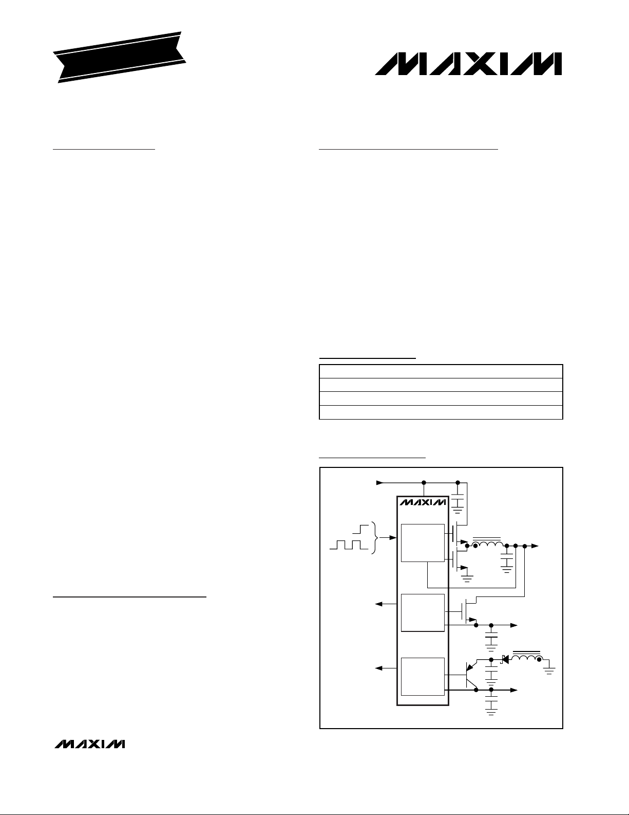
Functional Diagram
Ordering Information
19-3178; Rev 0; 2/04
For pricing, delivery, and ordering information, please contact Maxim/Dallas Direct! at
1-888-629-4642, or visit Maxim’s website at www.maxim-ic.com.
EVALUATION KIT
AVAILABLE
Pin Configurations appear at end of data sheet.
PART TEMP RANGE PIN-PACKAGE
MAX8513EEI -40°C to +85°C 28 QSOP
MAX8514EEI -40°C to +85°C 28 QSOP
MAX8514AEI -40°C to +125°C 28 QSOP
V
IN
(4.5V TO 28V)
ON
OFF
SYNC
MAX8513
STEPDOWN
CONTROLLER
V
OUT1
(1.25V TO 5.5V)
OUTPUT
POWER-ON RESET
LDO
CONTROLLER 1
INPUT POWER-
FAIL MONITOR
LDO
CONTROLLER 2
V
OUT2
(0.8V TO V
OUT1
V
OUT3
(0.8V TO 27V)
)
Page 2
MAX8513/MAX8514
Wide-Input, High-Frequency, Triple-Output Supplies
with Voltage Monitor and Power-On Reset
2 _______________________________________________________________________________________
ABSOLUTE MAXIMUM RATINGS
ELECTRICAL CHARACTERISTICS
(VIN= VLX= V
SUP2
= 12V, V
PVL
= V
BST
- VLX= V
DRV3P
= 5V, V
SUP3N
= 3.3V, V
DRV3N
= -5V, CVL= 4.7µF, C
REF
= 0.22µF, R
FREQ
=
15.0kΩ, T
A
= 0°C to +85°C, unless otherwise noted. Typical values are at TA= +25°C.)
Stresses beyond those listed under “Absolute Maximum Ratings” may cause permanent damage to the device. These are stress ratings only, and functional
operation of the device at these or any other conditions beyond those indicated in the operational sections of the specifications is not implied. Exposure to
absolute maximum rating conditions for extended periods may affect device reliability.
IN, DRV3P, SUP2 to GND.......................................-0.3V to +30V
DRV2 to GND ..........................................-0.3V to (V
SUP2
+ 0.3V)
DRV3N to GND......................(V
SUP3N
- 28V) to (V
SUP3N
+ 0.3V)
FREQ, PFI, PFO, POR, SUP3N, SYNC/EN,
CSP, CSN to GND ................................................-0.3V to +6V
VL to GND ...................-0.3V to the lesser of (V
IN
+ 0.3V) or +6V
COMP1, FB1, FB2, FB3P, FB3N, REF, ILIM,
SS, SEQ to GND......................................-0.3V to (V
VL
+ 0.3V)
PVL to PGND............................................................-0.3V to +6V
DL to PGND...............................................-0.3V to (V
PVL
+ 0.3V)
BST to LX..................................................................-0.3V to +6V
DH to LX....................................................-0.3V to (V
BST
+ 0.3V)
PGND to GND .......................................................-0.3V to +0.3V
VL Short Circuit to GND .............................................Continuous
Continuous Power Dissipation (T
A
= +70°C)
28-Pin QSOP (derate 10.8mW/°C above +70°C).........860mW
Operating Temperature Range
MAX8513EEI, MAX8514EEI.............................-40°C to +85°C
MAX8514AEI..................................................-40°C to +125°C
Junction Temperature......................................................+150°C
Storage Temperature Range .............................-65°C to +150°C
Lead Temperature (soldering, 10s) .................................+300°C
GENERAL
IN Operating Range
IN Supply Current
IN Shutdown Current V
VL REGULATOR
VL Output Voltage VIN = 6V to 28V, IVL = 0.1mA to 40mA 4.75 5 5.25 V
VL Dropout Voltage From IN to VL, VIN = 5V, IVL = 40mA 560 mV
VL Line Regulation VIN = 6V to 28V, IVL = 5mA 0.05 %
VL Undervoltage Threshold VL rising, V
OUT1 (BUCK CONVERTER)
Output Voltage Range V
FB1 Regulation Threshold V
Error-Amplifier Open-Loop
Voltage Gain
FB1 Input Bias Current I
Error-Amplifier Gain Bandwidth 25 MHz
DH Output-Resistance High R
DH Output-Resistance Low R
DL Output-Resistance High R
DL Output-Resistance Low R
Driver Dead Time t
PARAMETER SYMBOL CONDITIONS MIN TYP MAX UNITS
OUT1
FB1
A
VOL
FB1_BIAS
DH_HIGH
DH_LOW
DL_HIGH
DL_LOW
dt
IN = VL 4.5 5.5
= 1.3V, V
V
FB1
include switching current to PVL and BST,
SYNC/EN = VL
SYNC/EN
(Note 1) 1.25 5.50 V
V
FB1
Starts from VDL = 1V or (VDH - VLX) = 1V 50 ns
= 0, R
HYST
= 1.3V -200 +10 +200 nA
= V
FB2
FREQ
= 675mV (typ) 3.6 4.2 V
= 1.0V, does not
FB3
= 50kΩ 200 300 µA
5.5 28.0
2.6 3.2 mA
1.234 1.25 1.259 V
65 90 dB
1.5 2.55 Ω
1.2 2.1 Ω
2.5 5 Ω
0.7 1.3 Ω
V
Page 3

MAX8513/MAX8514
Wide-Input, High-Frequency, Triple-Output Supplies
with Voltage Monitor and Power-On Reset
_______________________________________________________________________________________ 3
ELECTRICAL CHARACTERISTICS (continued)
(VIN= VLX= V
SUP2
= 12V, V
PVL
= V
BST
- VLX= V
DRV3P
= 5V, V
SUP3N
= 3.3V, V
DRV3N
= -5V, CVL= 4.7µF, C
REF
= 0.22µF, R
FREQ
=
15.0kΩ, T
A
= 0°C to +85°C, unless otherwise noted. Typical values are at TA= +25°C.)
PARAMETER SYMBOL CONDITIONS MIN TYP MAX UNITS
Current-Limit Threshold (Positive) V
Current-Limit Threshold
(Negative)
CSP and CSN Bias Current V
ILIM Bias Current V
SS Soft-Start Charge Current VSS = 0.6V 15 25 35 µA
Soft-Start Discharge Resistance 100 200 Ω
LX, BST, PVL Leakage Current
FB1 Power-On Reset Threshold 1.08 1.125 1.20 V
OUT2 (POSITIVE LDO)
SUP2 Operating Range V
DRV2 Clamp Voltage V
SUP2 Supply Current 160 300 µA
SUP2 Shutdown Supply Current V
FB2 Regulation Voltage V
FB2 Input Bias Current I
DRV2 Output Current Limit VIN = 5V, V
DRV2 Output Current Limit
During Soft-Start
FB2 Power-On Reset Threshold 0.690 0.720 0.742 V
FB2 to DRV2 Transconductance G
OUT3P (POSITIVE PNP LDO) (MAX8513 ONLY)
DRV3P Operating Range V
FB3P Regulation Voltage V
FB3P to DRV3P Large-Signal
Transconductance
Feedback Input Bias Current V
Driver Sink Current V
FB3P POR Threshold 0.690 0.720 0.742 V
FB3P Soft-Start Period 1312
V
SUP2
DRV2
FB2
FB2_BIASVFB2
DRV3P
G
C3P
CS
CS
V
= 2.00V, V
ILIM
V
= 0.50V, V
ILIM
V
= VVL, V
ILIM
V
= 2.00V, V
ILIM
V
= 0.50V, V
ILIM
V
= VVL, V
ILIM
= V
CSP
ILIM
V
= VIN = 28V, V
LX
V
SYNC/EN
= 0 to 5.5V -120 +135 µA
CSN
= 1.25V -5.3 -5 -4.7 µA
= 0
= 0 to 5.5V 246 275 300
CSN
= 0 to 5.5V 50 67 81
CSN
= 0 to 5.5V 151 170 188
CSN
= 0 to 5.5V -333 -272 -199
CSN
= 0 to 5.5V -90 -67 -42
CSN
= 0 to 5.5V -210 -166 -122
CSN
= 33V, V
BST
= 5V,
PVL
0.03 20 µA
(Note 1) 4.5 28.0 V
V
= 0.75V 7.75 9.00 V
FB2
SYNC/EN
= 0 3 10 µA
0.784 0.80 0.808 V
= 0.75V 0.01 100 nA
C2
= 5V, V
DRV2
V
= 6V, V
IN
I
= +250µA, -250µA 0.12 0.2 0.36 S
DRV2
DRV2
= 5V, V
= 0.77V 15 30 mA
FB2
= 0.70V 8 10 12 mA
FB2
128V
= 5V, I
DRV3P
V
= 5V, I
DRV3P
= 0.75V 0.01 100 nA
FB3P
= 0.75V
FB3P
= 1mA 0.790 0.803 0.816 V
DRV3P
= 0.5mA to 5mA 0.38 0.6 1.1 S
DRV3P
DRV3P = 2.5V 15 35
DRV3P = 4.0V 40
Clock
Cycles
mV
mV
mA
Page 4
MAX8513/MAX8514
Wide-Input, High-Frequency, Triple-Output Supplies
with Voltage Monitor and Power-On Reset
4 _______________________________________________________________________________________
ELECTRICAL CHARACTERISTICS (continued)
(VIN= VLX= V
SUP2
= 12V, V
PVL
= V
BST
- VLX= V
DRV3P
= 5V, V
SUP3N
= 3.3V, V
DRV3N
= -5V, CVL= 4.7µF, C
REF
= 0.22µF, R
FREQ
=
15.0kΩ, T
A
= 0°C to +85°C, unless otherwise noted. Typical values are at TA= +25°C.)
PARAMETER SYMBOL CONDITIONS MIN TYP MAX UNITS
OUT3N (NEGATIVE NPN LDO CONTROLLER) (MAX8514 ONLY)
SUP3N Operating Range (Note 1) 1.5 5.5 V
DRV3N Operating Range (Note 1)
SUP3N Supply Current
FB3N Regulation Voltage
FB3N to DRV3N Large-Signal
Transconductance
Feedback Input Bias Current V
Driver Source Current
FB3N POR Threshold 450 500 550 mV
FB3N Soft-Start Period 2048
REFERENCE
REF Output Voltage V
OSCILLATOR
FREQ Resistance-Frequency
Product
Maximum Duty Cycle
(Measured at DH Pin)
Minimum On-Time
(Measured at DH Pin)
SYNC/EN Pulse Width Low or high (Note 1) 200 ns
SYNC/EN Frequency Range
SYNC/EN Input Voltage, High 2.4 V
SYNC/EN Input Voltage, Low 0.8 V
SYNC/EN Input Current V
G
C3N
REF
S
V
SUP3N
V
- 21V
V
= 1.5V, V
DRV3N
= -1mA (source)
I
DRV3N
V
= 1.5V, V
DRV3N
= -1mA (source)
I
DRV3N
V
= 0, I
DRV3N
DRV3N
(source)
= -100mV 60 1000 nA
FB3N
V
= 200mV, V
FB3N
= 3.5V
V
SUP3N
-2µA < I
R
FREQ
R
FREQ
R
FREQ
< +50µA 1.231 1.25 1.269 V
REF
= 10.7kΩ ±1% from FREQ to GND 1300 1390 1460
= 15.0kΩ ±1% from FREQ to GND 933 985 1040Frequency f
= 50.0kΩ ±1% from FREQ to GND 260 290 324
= 3.5V,
SUP3N
= 3.5V,
SUP3N
= -0.5mA to -5mA
= 0,
DRV3N
1.1 2 mA
-20 -5 +10 mV
0.225 0.36 0.550 S
13 25 mA
15.0
R
= 10.7kΩ ±1% from FREQ to GND 77 83 91
FREQ
R
= 15.0kΩ ±1% from FREQ to GND 80 87 95
FREQ
= 50.0kΩ ±1% from FREQ to GND 93 96 99
R
FREQ
R
= 10.7kΩ ±1% from FREQ to GND 20 62 ns
FREQ
SYNC/EN input frequency needs to be
within ±30% of the value set at the FREQ
200 1850 kHz
pin (Note 1)
= 0 to 5.5V -1 +1 µA
SYNC/EN
SUP3N
- 1.5V
V
Clock
Cycles
kHz
MHz
× kΩ
%
Page 5

MAX8513/MAX8514
Wide-Input, High-Frequency, Triple-Output Supplies
with Voltage Monitor and Power-On Reset
_______________________________________________________________________________________ 5
ELECTRICAL CHARACTERISTICS (continued)
(VIN= VLX= V
SUP2
= 12V, V
PVL
= V
BST
- VLX= V
DRV3P
= 5V, V
SUP3N
= 3.3V, V
DRV3N
= -5V, CVL= 4.7µF, C
REF
= 0.22µF, R
FREQ
=
15.0kΩ, T
A
= 0°C to +85°C, unless otherwise noted. Typical values are at TA= +25°C.)
ELECTRICAL CHARACTERISTICS
(VIN= VLX= V
SUP2
= 12V, V
PVL
= V
BST
- VLX= V
DRV3P
= 5V, V
SUP3N
= 3.3V, V
DRV3N
= -5V, CVL= 4.7µF, C
REF
= 0.22µF, R
FREQ
=
15.0kΩ, T
A
= -40°C to +125°C (Note 2), unless otherwise noted.)
PARAMETER SYMBOL CONDITIONS MIN TYP MAX UNITS
SEQ, PFI, PFO, POR
SEQ Input-Voltage High 2.4 V
SEQ Input-Voltage Low 0.8 V
SEQ Input Current V
POR Output-Voltage Low
POR Output Leakage Current
POR Power-Ready Delay Time
PFI Input Threshold Falling, V
PFI Input Bias Current V
PFO Output-Voltage Low PFI = 1.1V
PFO Output Leakage Current PFI = 1.4V, PFO = 5V 0.001 1 µA
THERMAL PROTECTION
Thermal Shutdown Junction temperature rising +170 °C
Thermal-Shutdown Hysteresis 25 °C
= 0 to V
V
V
V
SEQ
FB1
FB3N
FB1
, V
, V
VL
, V
FB2
FB3P
, out-of-regulation
, and V
FB2
regulation
From V
FB1
, V
FB2
regulation to POR = high impedance
HYST
= 1.0V 0.1 100 nA
PFI
110µA
I
= 1.6mA 10 200
or V
FB3P
POR
I
POR
V
IN
FB3N
or V
= 0.1mA,
= 1.0V
, in-
FB3N
, in-
20 200
0.001 1 µA
140 315 560 ms
,
FB3P
, and V
= 20mV 1.20 1.22 1.25 V
I
= 1.6mA 20 200
PFO
= 0.1mA,
I
PFO
V
IN
= 1.0V
10 200
mV
mV
PARAMETER SYMBOL CONDITIONS MIN MAX UNITS
GENERAL
IN Operating Range
IN Supply Current
IN Shutdown Current V
VL REGULATOR
VL Output Voltage VIN = 6V to 28V, IVL = 0.1mA to 40mA 4.75 5.25 V
VL Dropout Voltage From IN to VL, VIN = 5V, IVL = 40mA 610 mV
VL Undervoltage Threshold VL rising, V
5.5 28.0
IN = VL 4.5 5.5
= 1.3V, V
V
FB1
include switching current to PVL and BST,
FB2
= V
FB3
= 1.0V, does not
3.2 mA
SYNC/EN = VL
SYNC/EN
= 0, R
HYST
= 50kΩ 300 µA
FREQ
= 675mV (typ) 3.6 4.2 V
V
Page 6
MAX8513/MAX8514
Wide-Input, High-Frequency, Triple-Output Supplies
with Voltage Monitor and Power-On Reset
6 _______________________________________________________________________________________
ELECTRICAL CHARACTERISTICS (continued)
(VIN= VLX= V
SUP2
= 12V, V
PVL
= V
BST
- VLX= V
DRV3P
= 5V, V
SUP3N
= 3.3V, V
DRV3N
= -5V, CVL= 4.7µF, C
REF
= 0.22µF, R
FREQ
=
15.0kΩ, T
A
= -40°C to +125°C (Note 2), unless otherwise noted.)
PARAMETER SYMBOL CONDITIONS MIN MAX UNITS
OUT1 (BUCK CONVERTER)
Output Voltage Range V
FB1 Regulation Threshold V
Error-Amplifier Open-Loop
Voltage Gain
FB1 Input Bias Current I
DH Output-Resistance High R
DH Output-Resistance Low R
DL Output-Resistance High R
DL Output-Resistance Low R
Current-Limit Threshold
(Positive)
Current-Limit Threshold
(Negative)
CSP and CSN Bias Current V
ILIM Bias Current V
SS Soft-Start Charge Current VSS = 0.6V 15 35 µA
Soft-Start Discharge Resistance 200 Ω
LX, BST, PVL Leakage Current
FB1 Power-On Reset Threshold 1.08 1.20 V
OUT2 (POSITIVE LDO)
SUP2 Operating Range V
DRV2 Clamp Voltage V
SUP2 Supply Current 300 µA
SUP2 Shutdown Supply Current V
FB2 Regulation Voltage V
FB2 Input Bias Current I
DRV2 Output Current Limit VIN = 5V, V
DRV2 Output Current Limit
During Soft-Start
FB2 Power-On Reset Threshold 0.690 0.742 V
FB2 to DRV2 Transconductance G
OUT1
FB1
A
VOL
FB1_BIASVFB1
DH_HIGH
DH_LOW
DL_HIGH
DL_LOW
V
CS
V
CS
SUP2
DRV2
FB2
FB2_BIASVFB2
C2
(Note 1) 1.25 5.50 V
1.225 1.265 V
65 dB
= 1.3V -200 +200 nA
2.55 Ω
2.1 Ω
5 Ω
1.3 Ω
V
= 2.00V, V
ILIM
V
= 0.50V, V
ILIM
V
= VVL, V
ILIM
V
= 2.00V, V
ILIM
V
= 0.50V, V
ILIM
V
= VVL, V
ILIM
= V
CSP
CSN
= 1.25V -5.7 -4.3 µA
ILIM
V
= VIN = 28V, V
LX
V
SYNC/EN
= 0
= 0 to 5.5V 243 303
CSN
= 0 to 5.5V 49 83
CSN
= 0 to 5.5V 147 190
CSN
= 0 to 5.5V -333 -199
CSN
= 0 to 5.5V -90 -42
CSN
= 0 to 5.5V -210 -122
CSN
= 0 to 5.5V -120 +135 µA
BST
= 33V, V
PVL
= 5V,
20 µA
(Note 1) 4.5 28.0 V
V
= 0.75V 7.75 9.00 V
FB2
SYNC/EN
= 0 10 µA
0.775 0.816 V
= 0.75V 150 nA
= 5V, V
DRV2
= 6V, V
V
IN
I
= +250µA, -250µA 0.11 0.41 S
DRV2
DRV2
= 5V, V
= 0.77V 12 mA
FB2
= 0.70V 8 12 mA
FB2
mV
mV
Page 7
MAX8513/MAX8514
Wide-Input, High-Frequency, Triple-Output Supplies
with Voltage Monitor and Power-On Reset
_______________________________________________________________________________________ 7
ELECTRICAL CHARACTERISTICS (continued)
(VIN= VLX= V
SUP2
= 12V, V
PVL
= V
BST
- VLX= V
DRV3P
= 5V, V
SUP3N
= 3.3V, V
DRV3N
= -5V, CVL= 4.7µF, C
REF
= 0.22µF, R
FREQ
=
15.0kΩ, T
A
= -40°C to +125°C (Note 2), unless otherwise noted.)
PARAMETER SYMBOL CONDITIONS MIN MAX UNITS
OUT3P (POSITIVE PNP LDO) (MAX8513 ONLY)
DRV3P Operating Range V
FB3P Regulation Voltage V
FB3P to DRV3P Large-Signal
Transconductance
Feedback Input Bias Current V
Driver Sink Current V
FB3P POR Threshold 0.690 0.742 V
OUT3N (NEGATIVE NPN LDO CONTROLLER) (MAX8514 ONLY)
SUP3N Operating Range (Note 1) 1.5 5.5 V
DRV3N Operating Range (Note 1)
SUP3N Supply Current
FB3N Regulation Voltage
FB3N to DRV3N Large-Signal
Transconductance
Feedback Input Bias Current V
Driver Source Current
FB3N POR Threshold 450 550 mV
REFERENCE
REF Output Voltage V
OSCILLATOR
Frequency f
Maximum Duty Cycle
(Measured at DH Pin)
Minimum On-Time
(Measured at DH Pin)
SYNC/EN Pulse Width Low or high (Note 1) 200 ns
SYNC/EN Frequency Range
DRV3P
G
C3PVDRV3P
G
C3N
REF
S
128V
= 5V, I
DRV3P
= 5V, I
= 0.75V 100 nA
FB3P
= 0.75V DRV3P = 2.5V 15 mA
FB3P
V
= 1.5V, V
DRV3N
I
= -1mA (source)
DRV3N
V
= 1.5V, V
DRV3N
I
= -1mA (source)
DRV3N
V
= 0, I
DRV3N
(source)
= -100mV 1500 nA
FB3N
V
= 200mV, V
FB3N
= 3.5V
V
SUP3N
-2µA < I
R
FREQ
R
FREQ
R
FREQ
R
FREQ
R
FREQ
R
FREQ
R
FREQ
< +50µA 1.22 1.27 V
REF
= 10.7kΩ ±1% from FREQ to GND 1300 1500
= 15.0kΩ ±1% from FREQ to GND 917 1070
= 50.0kΩ ±1% from FREQ to GND 250 335
= 10.7kΩ ±1% from FREQ to GND 77 91
= 15.0kΩ ±1% from FREQ to GND 80 95
= 50.0kΩ ±1% from FREQ to GND 93 99
= 10.7kΩ ±1% from FREQ to GND 62 ns
= 1mA 0.780 0.820 V
DRV3P
= 0.5mA to 5mA 0.3 1.4 S
DRV3P
V
SUP3N
- 21V
= 3.5V,
SUP3N
= 3.5V,
SUP3N
= -0.5mA to -5mA
DRV3N
DRV3N
= 0,
-20 +10 mV
0.225 0.550 S
13 mA
V
SUP3N
- 1.5V
SYNC/EN input frequency needs to be
within ±30% of the value set at the FREQ
200 1850 kHz
pin (Note 1)
2mA
V
kHz
%
Page 8
MAX8513/MAX8514
Wide-Input, High-Frequency, Triple-Output Supplies
with Voltage Monitor and Power-On Reset
8 _______________________________________________________________________________________
ELECTRICAL CHARACTERISTICS (continued)
(VIN= VLX= V
SUP2
= 12V, V
PVL
= V
BST
- VLX= V
DRV3P
= 5V, V
SUP3N
= 3.3V, V
DRV3N
= -5V, CVL= 4.7µF, C
REF
= 0.22µF, R
FREQ
=
15.0kΩ, T
A
= -40°C to +125°C (Note 2), unless otherwise noted.)
Note 1: Guaranteed by design, not production tested.
Note 2: Specifications to -40°C are guaranteed by design, not production tested.
SYNC/EN Input-Voltage High 2.4 V
SYNC/EN Input-Voltage Low 0.8 V
SYNC/EN Input Current V
SEQ, PFI, PFO, POR
SEQ Input-Voltage High 2.4 V
SEQ Input-Voltage Low 0.8 V
SEQ Input Current V
POR Output-Voltage Low
POR Output Leakage Current
PARAMETER SYMBOL CONDITIONS MIN MAX UNITS
POR Power-Ready Delay Time
PFI Input Threshold Falling, V
PFI Input Bias Current V
PFO Output-Voltage Low PFI = 1.1V
PFO Output Leakage Current PFI = 1.4V, PFO = 5V 1 µA
SYNC/EN
SEQ
V
FB1
V
FB3N
V
FB1
regulation
From V
regulation to POR = high impedance
PFI
= 0 to 5.5V -1 +1 µA
= 0 to V
VL
, V
, V
FB2
FB3P
out-of-regulation
, V
, and V
FB2
, V
FB1
FB2
HYST
= 1.0V 300 nA
I
or V
FB3P
POR
I
POR
V
IN
FB3N
or V
I
PFO
I
PFO
V
IN
= 1.0V
= 1.0V
,
FB3P
, and V
= 20mV 1.20 1.25 V
= 1.6mA 200
= 0.1mA,
, in-
, in-
FB3N
= 1.6mA 200
= 0.1mA,
140 560 ms
10 µA
200
1µA
200
mV
mV
Page 9
MAX8513/MAX8514
Wide-Input, High-Frequency, Triple-Output Supplies
with Voltage Monitor and Power-On Reset
_______________________________________________________________________________________ 9
Typical Operating Characteristics
(Circuit of MAX8513 evaluation kit, VIN= 12V, TA= +25°C, fS= 1.4MHz, unless otherwise noted.)
EFFICIENCY vs. INPUT VOLTAGE
EFFICIENCY vs. I
100
90
80
70
60
50
40
EFFICIENCY (%)
30
V
= 3.3V, I
OUT1
(V)
OUT2
V
20
10
0
2.55
2.54
2.53
2.52
2.51
2.50
2.49
2.48
2.47
2.46
2.45
= 2.5V, I
V
OUT2
= 12V, I
V
OUT3
718
V
= 3.3V AT 1A
OUT1
= 12V AT 25mA
V
OUT3
0
V
OUT1
OUT2
OUT3
OUT2
= 2A
= 1.5A
= 50mA
VIN (V)
vs. I
0.8
I
OUT2
(A)
OUT2
171614 159 10 11 12 138
1.4
1.2
1.00.4 0.60.2
MAX8513/14 toc01
MAX8513/14 toc04
100
90
80
70
60
50
40
EFFICIENCY (%)
12.25
12.20
12.15
12.10
12.05
(V)
12.00
OUT3
V
11.95
11.90
11.85
11.80
11.75
VIN = 16V
30
20
10
0
0.1
V
= 3.3V AT 1A
OUT1
= 2.5V AT 0.75A
V
OUT2
050
(I
OUT2
VIN = 12V
V
= 0, I
OUT3
I
I
OUT3
VIN = 9V
OUT1
vs. I
OUT3
(A)
(mA)
OUT3
OUT1
= 0)
3.35
3.34
3.33
MAX8513/14 toc02
3.32
3.31
(V)
3.30
OUT1
V
3.29
3.28
3.27
3.26
MAX8513/14 toc05
(V)
OUT1
V
3.25
3.35
3.34
3.33
3.32
3.31
3.30
3.29
3.28
3.27
3.26
3.25
4.1
3.6
3.12.1 2.61.1 1.60.6
454030 3510 15 20 255
V
vs. I
OUT1
V
= 2.5V AT 0.75A
OUT2
= 12V AT 25mA
V
OUT3
0
V
V
= 2.5V AT 0.75A
OUT2
= 12V AT 25mA
V
OUT3
718
OUT1
I
I
OUT1
OUT1
I
OUT1
VIN (V)
(A)
vs. V
= 0
= 3A
OUT1
IN
MAX8513/14 toc03
4.0
3.5
3.02.0 2.51.0 1.50.5
MAX8513/14 toc06
171614 159 10 11 12 138
V
vs. V
2.55
V
OUT1
2.54
V
OUT3
2.53
2.52
2.51
(V)
2.50
OUT2
V
2.49
2.48
2.47
2.46
2.45
718
OUT2
= 3.3V AT 1A
= 12V AT 25mA
I
OUT2
I
OUT2
VIN (V)
IN
= 0
= 1.5A
171614 159 10 11 12 138
MAX8513/14 toc07
12.35
V
= 3.3V AT 1A
OUT1
12.30
12.25
12.20
12.15
(V)
12.10
OUT3
V
12.05
12.00
11.95
11.90
11.85
= 2.5V AT 0.75A
V
OUT2
718
V
OUT3
I
vs. V
OUT3
I
OUT3
VIN (V)
= 0
= 50mA
OSCILLATOR FREQUENCY
IN
171614 159 10 11 12 138
1.43
1.42
MAX8513/14 toc08
1.41
1.40
1.39
1.38
1.37
OSCILLATOR FREQUENCY (MHz)
1.36
1.35
718
vs. INPUT VOLTAGE
R
= 10.7kΩ
FREQ
TA = -40°C
TA = +85°C
VIN (V)
TA = +25°C
MAX8513/14 toc09
171614 159 10 11 12 138
Page 10
MAX8513/MAX8514
Wide-Input, High-Frequency, Triple-Output Supplies
with Voltage Monitor and Power-On Reset
10 ______________________________________________________________________________________
Typical Operating Characteristics (continued)
(Circuit of MAX8513 evaluation kit, VIN= 12V, TA= +25°C, fS= 1.4MHz, unless otherwise noted.)
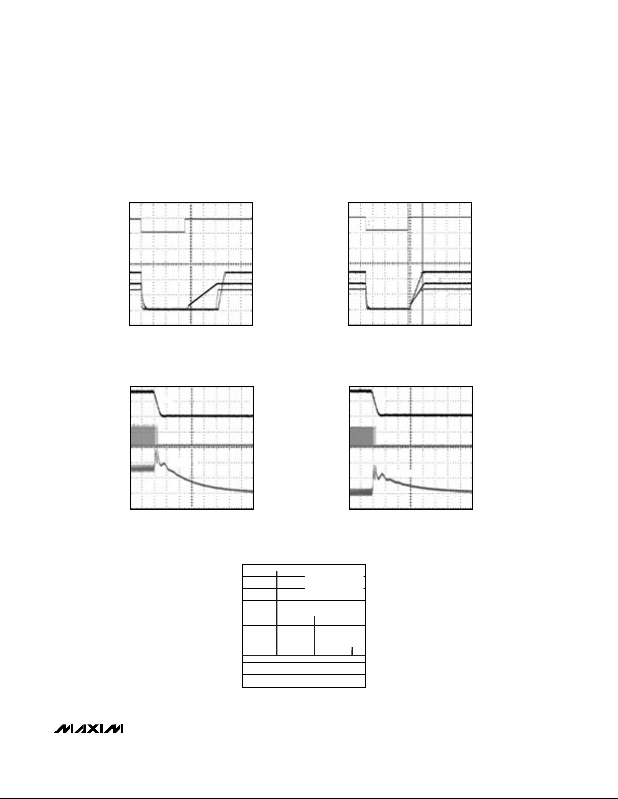
OUTPUT1 LOAD-TRANSIENT RESPONSE
I
50mV/div
50mV/div
100mV/div
0A
OUT2
= 0.75A, I
OUT3
= 25mA
40µs/div
MAX8513/14 toc10
SWITCHING WAVEFORMS
(ALL OUTPUTS AT FULL LOAD)
0V
0V
0V
0V
MAX8513/14 toc12
V
OUT1
AC-COUPLED
V
OUT2
AC-COUPLED
V
OUT3
AC-COUPLED
I
OUT1
1A/div
V
DH
10V/div
V
DL
5V/div
V
LX
10V/div
V
D2
(ANODE)
20V/div
OUTPUT3 LOAD-TRANSIENT RESPONSE
I
= 1A, I
OUT2
= 0.75A
40µs/div
OUT1
50mV/div
50mV/div
50mV/div
5mA
SYNCHRONIZATION
0V
0V
0V
MAX8513/14 toc11
MAX8513/14 toc13
V
OUT1
AC-COUPLED
V
OUT2
AC-COUPLED
V
OUT3
AC-COUPLED
I
OUT3
50mA/div
V
DH
5V/div
V
DL
10V/div
SYNC/EN
5V/div
200ns/div
PFO RESPONSE
0V
0V
0V
I
= 2A, I
OUT2
= 1.5A, I
2ms/div
OUT1
OUT3
= 50mA
MAX8513/14 toc14
PFO
2V/div
V
IN
5V/div
V
OUT1
2V/div
0V
0V
0V
0V
1µs/div
POR RESPONSE
100ms/div
MAX8513/14 toc15
POR
5V/div
V
OUT1
2V/div
V
OUT2
5V/div
V
OUT3
10V/div
Page 11
MAX8513/MAX8514
Wide-Input, High-Frequency, Triple-Output Supplies
with Voltage Monitor and Power-On Reset
______________________________________________________________________________________ 11
Typical Operating Characteristics (continued)
(Circuit of MAX8513 evaluation kit, VIN= 12V, TA= +25°C, fS= 1.4MHz, unless otherwise noted.)
STAGGERED SEQUENCE (SEQ = GND)
0V
0V
2ms/div
OUTPUT1 SHORT CIRCUIT
(ALL OUTPUTS AT FULL LOAD)
0V
0V
0A
MAX8513/14 toc16
MAX8513/14 toc18
SYNC/EN
5V/div
V
OUT3
5V/div
V
OUT1
2V/div
V
OUT2
2V/div
V
OUT1
2V/div
V
LX
10V/div
1
L
2A/div
TRACKING SEQUENCE (SEQ = VL)
0V
0V
4ms/div
OUTPUT1 SHORT CIRCUIT
(ALL OUTPUTS AT NO LOAD)
0V
0V
0A
MAX8513/14 toc17
MAX8513/14 toc19
SYNC/EN
5V/div
V
OUT3
5V/div
V
OUT1
2V/div
V
OUT2
2V/div
V
OUT1
2V/div
V
LX
10V/div
I
L
2A/div
20µs/div
20µs/div
OUTPUT RIPPLE AND HARMONICS
(MEASURED AT OUT1)
1.5
1.3
1.1
0.9
0.7
0.5
NOISE (mV)
0.3
0.1
-0.1
-0.3
-0.5
100 21001100 3100 4100 5100
VIN = 12V
V
OUT1
V
OUT2
V
OUT3
FREQUENCY (kHz)
= 3.3V AT 2A
= 2.5V AT 1.5A
= 12V AT 50mA
MAX8513/14 toc20
Page 12

MAX8513/MAX8514
Wide-Input, High-Frequency, Triple-Output Supplies
with Voltage Monitor and Power-On Reset
12 ______________________________________________________________________________________
Pin Description
PIN
NAME
MAX8513 MAX8514 FUNCTION
Power-Fail Input. Connect PFI to an external resistive-divider between IN, PFI, and GND.
PFI 1 1
PFI senses V
20mV of hysteresis.
to detect voltage failure. Trip falling threshold at this input is 1.22V, with
IN
PFO 2 2 Power-Fail Output. Open-drain output that goes low if V
DH 3 3
LX 4 4
BST 5 5
DL 6 6
PVL 7 7
OUT1 High-Side Gate-Drive Output. DH drives the high-side N-channel MOSFET (Q1 in the
Typical Applications Circuits). DH is a floating driver output that swings from LX to BST.
OUT1 High-Side Driver Return Path. The high-side FET driver uses BST and LX for its
respective high and low-side supplies.
OUT1 Boost Capacitor Connection for High-Side Gate Drive. Connect a 0.1µF ceramic
capacitor from BST to LX with a less than 5mm trace length.
OUT1 Low-Side Gate-Drive Output. DL drives the low-side N-channel MOSFET (Q2 in the
Typical Applications Circuits). DL swings from 0 to V
OUT1 Gate-Drive Supply Bypass Connection. Connect PVL to VL through a 10Ω resistor
(R15), and bypass PVL to PGND with a minimum 1µF capacitor (C1).
PGND 8 8 Power-Ground Connection and Low-Side Supply for Dl Driver
Internal +5V Linear-Regulator Bypass Pin. Bypass VL to GND with a minimum 2.2µF
VL 9 9
ceramic capacitor (C10) and 5mm or less of trace length. VL should be connected to IN
when V
< 5.5V.
IN
COMP1 10 10 OUT1 Compensation Node. See the OUT1 Compensation section.
FB1 11 11
OUT1 Feedback Input. Connect a resistive-divider (R1, R2) from OUT1 to FB1 to GND to
regulate FB1 at 1.25V.
PVL
< 1.22V.
PFI
.
Oscillator Frequency-Set Input. A resistor from FREQ to GND sets the oscillator frequency
FREQ 12 12
from 300kHz to 1.4MHz (f = 15MHz x kΩ / R
is used at SYNC/EN, and the SYNC/EN input frequency should be within ±30% of the
frequency set by R
FREQ
.
FREQ
). R
is still required if an external clock
FREQ
REF 13 13 1.25V Refer ence O utp ut. C onnect a 0.1µF or l ar g er cer am i c cap aci tor ( C 9) fr om RE F to GN D .
GND 14 14 Analog/Signal Ground
FB2 15 15
DRV2 16 16
SUP2 17 17
OUT2 Feedback Input. Connect a resistive-divider (R5, R6) from OUT2 to FB2 to GND to
regulate FB2 to 0.8V.
OUT2 Gate Drive. DRV2 connects to the gate of an external N-channel MOSFET to form a
positive linear voltage regulator.
Supply Input for DRV2. Connect to a voltage source of at least 1V above the maximum
desired DRV2 gate voltage.
Page 13
MAX8513/MAX8514
Wide-Input, High-Frequency, Triple-Output Supplies
with Voltage Monitor and Power-On Reset
______________________________________________________________________________________ 13
Pin Description (continued)
PIN
NAME
MAX8513 MAX8514 FUNCTION
Connect to VL for output tracking. Connect to GND for output staggered sequence.
SEQ 18 18
SYNC/EN 19 19
Staggered sequence ramps up V
voltage due to charging of the LDO’s output capacitors.
Shutdown Control and Synchronization Input. There are three operating modes:
• When SYNC/EN is low, the controller is off but the VL regulator is still running.
• When SYNC/EN is high, the controller is enabled with the switching frequency set by
R
• When SYNC/EN is driven by an external clock, the controller is enabled and switches at
the external clock frequency.
FREQ
.
OUT2
and V
softly to avoid glitches on the previous
OUT3
N.C. 20 — No Connection. Not internally connected. Connect to GND or leave floating.
SUP3N — 20
DRV3P 21 —
DRV3N — 21
IN 22 22
POR 23 23
FB3P 24 —
FB3N — 24
ILIM 25 25
OUT3N Base-Drive Supply. Connect SUP3N to any positive voltage between 1.5V and 5.5V
to provide power for the negative linear-regulator transistor driver.
OUT3P Base Drive. Connect DRV3P to the base of an external PNP pass transistor to form a
positive linear voltage regulator.
OUT3N Base Drive. Connect DRV3N to the base of an external NPN pass transistor to form
a negative linear voltage regulator.
Main Voltage Input (4.5V to 28V). Bypass IN to GND, close to the IC, with a minimum 1µF
ceramic capacitor (C2). IN powers the linear regulator whose output is VL.
Power-On Reset. Open-drain output that goes high after all outputs reach the regulation
limit and a 315ms delay time has elapsed.
OUT3P Feedback Input. FB3P is referenced to 0.8V and connects to a resistive-divider
(R13, R14) to control a positive linear voltage regulator.
OUT3N Feedback Input. Connect a resistive-divider (R13, R14) from OUT1 to FB3N to
OUT3N to regulate FB3N to 0V.
ILIM Set Input. Connect a resistive-divider (R17, R18) from OUT1 to ILIM to GND. See the
Current Limit section.
CSP 26 26 Positive Current-Sense Input. Used to detect OUT1 current limit.
CSN 27 27 Negative Current-Sense Input. Used to detect OUT1 current limit.
Anal og S oft- S tar t C ontr ol Inp ut. Thi s p i n g oes i nto the p osi ti ve i np ut of the V OU T1’ s er r or
SS 28 28
am p l i fi er . W hen the M AX 8513/M AX 8514 ar e tur ned on, S S i s at GN D and char g es up to 1.25V
w i th a constant 25µA. C onnect a cap aci tor ( C 13) fr om S S to G N D for the d esi r ed soft- star t ti m e.
Page 14
MAX8513/MAX8514
Wide-Input, High-Frequency, Triple-Output Supplies
with Voltage Monitor and Power-On Reset
14 ______________________________________________________________________________________
Figure 1. MAX8513 Functional Diagram
IN
SS
BST
SYNC/EN
VL
GND
FREQ
SEQ
BIAS
PWM
COMP.
1V
PFI
PFO
N
POR
N
REF
REFERENCE
SRQ
Q
1/7.5
P-P
1.25V
0.8V
G
C3P
ERROR
AMP
5µA
0.8V
N
G
C2
DH
LX
PVL
DL
PGND
CSP
CSN
FB1
COMP
ILIM
SUP2
DRV2
FB2
DRV3P
N
FB3P
MAX8513
Page 15

MAX8513/MAX8514
Wide-Input, High-Frequency, Triple-Output Supplies
with Voltage Monitor and Power-On Reset
______________________________________________________________________________________ 15
Figure 2. MAX8514 Functional Diagram
SYNC/EN
GND
FREQ
SEQ
PFO
POR
SS
PFI
IN
BST
SRQ
Q
VL
BIAS
1/7.5
PWM
COMP.
1V
P-P
1.25V
N
REFERENCE
N
ERROR
AMP
5µA
0.8V
G
C2
DH
LX
PVL
DL
PGND
CSP
CSN
FB1
COMP
ILIM
SUP2
DRV2
FB2
REF
MAX8514
SUP3N
G
C3N
P
P
DRV3N
FB3N
Page 16

MAX8513/MAX8514
Wide-Input, High-Frequency, Triple-Output Supplies
with Voltage Monitor and Power-On Reset
16 ______________________________________________________________________________________
Detailed Description
The MAX8513/MAX8514 combine a step-down DC-DC
converter and two LDOs, providing three output voltages for xDSL modem and set-top box applications.
The switching frequency is set with an external resistor
connected from the FREQ pin to GND, and is
adjustable from 300kHz to 1.4MHz. The main stepdown DC-DC controller operates in a voltage-mode,
pulse-width-modulation (PWM) control scheme. The
MAX8513/MAX8514 include two low-cost LDO controllers capable of delivering current from the DC-DC
main output, an extra winding, the input, or from an
alternate supply voltage. The first LDO controller drives
an external NMOS or NPN with a maximum drive of
7.75V. The second LDO controller provides either a
positive 0.8V to 27V output using an external PNP pass
device, or a negative -1V to -18V output with an external NPN pass device.
DC-DC Controller
The MAX8513/MAX8514 step-down DC-DC converters
use a PWM voltage-mode control scheme. An internal
high-bandwidth (25MHz) operational amplifier is used
as an error amplifier to regulate the output voltage. The
output voltage is sensed and compared with an internal
1.25V reference to generate an error signal. The error
signal is then compared with a fixed-frequency ramp
by a PWM comparator to give the appropriate duty
cycle to maintain output-voltage regulation. At the rising edge of the internal clock and when DL (the lowside MOSFET gate drive) is at 0V, the high-side
MOSFET turns on. When the ramp voltage reaches the
error-amplifier output voltage, the high-side MOSFET
latches off until the next clock pulse. During the highside MOSFET on-time, current flows from the input
through the inductor to the output capacitor and load.
At the moment the high-side MOSFET turns off, the
energy stored in the inductor during the on-time is
released to support the load. The inductor current
ramps down through the low-side MOSFET body diode.
After a fixed delay, the low-side MOSFET turns on to
shunt the current from its body diode for a lower voltage
drop to increase the efficiency. The low-side MOSFET
turns off at the rising edge of the next clock pulse, and
when its gate voltage discharges to zero, the high-side
MOSFET turns on after an additional fixed delay and
another cycle starts.
The MAX8513/MAX8514 operate in forced-PWM mode,
so even under light load the controller maintains a constant switching frequency to minimize noise and possible interference with system circuitry.
Current Limit
The MAX8513/MAX8514s’ switching regulator senses
the inductor current either through the DC resistance of
the inductor itself for lossless sensing, or through a
series resistor for more accurate sensing. When using
the DC resistance of the inductor, an RC filter circuit is
needed (see R19, R20, and C14 of the Typical
Applications Circuits and the Current-Limit Setting section). When peak voltage across the sensing circuit
(which occurs at the peak of the inductor current)
exceeds the current-limit threshold set by ILIM, the
controller turns off the high-side MOSFET and turns on
the low-side MOSFET. The inductor current ramps
down and DH turns on again if the inductor current is
below the current-limit threshold at the next clock
pulse. The MAX8513/MAX8514 current-limit threshold
can be set by two external resistors to be proportional
to the output voltage with an adjustable offset level,
providing foldback current-limit and short-circuit protection. This feature greatly reduces power dissipation
and prevents overheating of external components during an indefinite short-circuit at the output. See the
Foldback Current Limit section for how to set ILIM with
external resistors. The current-limit threshold defaults to
170mV when ILIM is connected to VL, and in this case,
the current limit functions as a constant current limit
only. The LDO controllers do not have current limit and
rely on input current limit for protection.
Synchronous-Rectifier Driver (DL)
Synchronous rectification reduces the conduction loss
in the rectifier by replacing the normal Schottky catch
diode with a low-on-resistance MOSFET switch. The
MAX8513/MAX8514 also use the synchronous rectifier
to ensure proper startup of the boost gate-drive circuit.
High-Side Gate-Drive Supply (BST)
A flying-capacitor boost circuit (see D1 and C3 in the
Typical Applications Circuits) generates the gate-drive
voltage for the high-side N-channel MOSFET. On startup, the synchronous rectifier (low-side MOSFET, Q2)
forces LX to ground and charges the boost capacitor
(C3) to VVL- V
DIODE
. On the second half-cycle, the
controller turns on the high-side MOSFET by closing an
internal switch between BST and DH. This boosts the
voltage at BST to VVL- V
DIODE
+ VIN, providing the
necessary gate-to-source voltage to turn on the highside N-channel MOSFET.
Page 17

MAX8513/MAX8514
Wide-Input, High-Frequency, Triple-Output Supplies
with Voltage Monitor and Power-On Reset
______________________________________________________________________________________ 17
Internal 5V Linear Regulator
All MAX8513/MAX8514 functions (except for the positive output LDO with an NFET or NPN, and the negative
LDO on the MAX8514) are powered from the on-chip
low-dropout 5V regulator with its input connected to IN.
Bypass the regulator’s output (VL) with a 2.2µF or
greater ceramic capacitor. The VINto VVLdropout voltage is typically 350mV, so when VINis greater than
5.5V, VVLis typically 5V. If VINis between 4.5V and
5.5V, short VL to IN.
Undervoltage Lockout
If VVLdrops below 3.8V, the MAX8513/MAX8514
assume that the supply voltage is too low to make valid
decisions. When this happens, the undervoltage lockout (UVLO) circuitry inhibits switching, forces POR and
PFO low, and forces DL and DH gate drivers low. After
VVLrises above 3.9V, the controller powers up the outputs (see the Startup section).
Startup
The MAX8513/MAX8514 start switching when VVLrises
above the 3.9V UVLO threshold. However, the controller is not enabled unless all three of the following
conditions are met:
1) VVLexceeds the 3.9V UVLO threshold.
2) The internal reference exceeds 90% of its nominal
value.
3) The thermal limit is not exceeded.
Once the MAX8513/MAX8514 assert the internal enable
signal, the step-down controller starts switching and
enables soft-start. The soft-start circuitry gradually ramps
up to the reference voltage to control the rate-of-rise of
the step-down controller and reduce input surge currents. The soft-start period is determined by the value of
the capacitor from SS to GND (C13 in the Typical
Applications Circuits). SS sources a constant 25µA to
charge the soft-start capacitor to 1.25V.
Output-Voltage Sequencing
The MAX8513/MAX8514 can power up in either staggered-output sequencing or output tracking. For staggered-output sequencing, connect SEQ to GND. In this
configuration, V
OUT1
comes up first. When it reaches
90% of the nominal regulated value, V
OUT2
is softly
turned on. Once V
OUT2
reaches 90% of its nominal regu-
lated value, V
OUT3
is softly turned on. Individual soft-start
on OUT2 and OUT3 eliminates glitches on the previous
stages due to the charging of output capacitors. See the
Typical Operating Characteristics section for the startup
and staggered-output-sequence waveforms.
Output-Voltage Tracking
When SEQ is connected to VL, all outputs rise up at the
same time and the external series pass transistors are
driven fully on until reaching the respective regulation
limits. Since the LDOs are powered from the main DCDC step-down converter, either directly or through a
coupled winding on the inductor, their outputs track the
DC-DC step-down output (OUT1). See the Typical
Operating Characteristics section for the startup outputtracking waveforms.
Power-On Reset
The MAX8513/MAX8514 provide a power-on-reset (POR)
signal, which goes high 315ms after all outputs reach
90% of their nominal regulated value. Therefore, by the
time POR goes high, all outputs are already stabilized at
nominal regulated voltages. See the Typical Operating
Characteristics section for the POR waveforms.
Input Power-Fail (PFI and PFO)
The MAX8513/MAX8514 have a built-in comparator to
detect the input voltage with an external resistivedivider at PFI, with a threshold of 1.22V. When the input
voltage drops and trips this comparator, the power-fail
output (PFO) goes low, while all outputs are still within
regulation limits. This is typically used for input powerfail warning for orderly system shutdown. The amount of
warning time depends on the input storage capacitor,
the input PFI trip voltage level, the main step-down output voltage, the total output power, and the efficiency.
See the Design Procedure section for how to calculate
the input capacitor to meet the required warning time.
Enable and Synchronization
The MAX8513/MAX8514 can be turned on with logic
high, and off with logic low at SYNC/EN. When SYNC/EN
is driven with an external clock, the internal oscillator
synchronizes the rising edge of the clock at SYNC/EN to
DH going high. When being driven by a synchronization
clock signal at SYNC/EN, the controller synchronizes to
the external clock within two cycles. The frequency at
SYNC/EN needs to be within ±30% of the value set by
R
FREQ
. See the Switching-Frequency Setting section.
Page 18

MAX8513/MAX8514
Wide-Input, High-Frequency, Triple-Output Supplies
with Voltage Monitor and Power-On Reset
18 ______________________________________________________________________________________
Thermal-Overload Protection
Thermal-overload protection limits the total power dissipation in the MAX8513/MAX8514. When the junction
temperature exceeds TJ= +170°C, a thermal sensor
shuts down the device, forcing DL and DH low and
allowing the IC to cool. The thermal sensor turns the part
on again after the junction temperature cools by 25°C,
resulting in a pulsed output during continuous thermaloverload conditions. During a thermal event, the main
step-down converter and the linear regulators are turned
off, POR and PFO go low, and soft-start is reset.
Design Procedure
OUT1 Voltage Setting
The output voltage is set by a resistive-divider network
from OUT1 to FB1 to GND (see R1 and R2 in the
Typical Applications Circuits). Select R2 between 5kΩ
and 15kΩ. Then R1 can be calculated by:
Input Power-Fail Setting
The PFI input can monitor V
IN
to determine if it is falling.
When the voltage at PFI crosses 1.22V, the output
(PFO) goes low. The input voltage value at the PFI trip
threshold, V
PFI
, is set by a resistive-divider network
from IN to PFI to GND (see the Typical Applications
Circuits). Select R11, the resistor from PFI to GND
between 10kΩ and 40kΩ. Then R10, the resistor from
PFI to IN, is calculated by:
Switching-Frequency Setting
The resistor connected from FREQ to GND, R
FREQ
(R7
in the Typical Applications Circuits), sets the switching
frequency, fS, as shown by the equation below:
where R
FREQ
is in ohms.
Inductor Value
There are several parameters that must be examined
when determining which inductor to use: input voltage,
output voltage, load current, switching frequency, and
LIR. LIR is the ratio of peak-to-peak inductor ripple current to the maximum DC load current. A higher LIR
value allows for a smaller inductor but results in higher
losses and higher output ripple. A good compromise
between size and efficiency is a 30% LIR. Once all of
the parameters are chosen, the inductor value is determined as follows:
where V
OUT1
is the main switching regulator output and
fS is the switching frequency.
Choose a standard value close to the calculated value.
The exact inductor value is not critical and can be
adjusted to make tradeoffs between size, cost, and efficiency. Lower inductor values minimize size and cost,
but also increase the output ripple and reduce the efficiency due to higher peak currents. On the other hand,
higher inductor values increase efficiency, but eventually resistive losses due to extra turns of wire exceed the
benefit gained from lower AC current levels. Find a lowloss inductor with the lowest possible DC resistance that
fits the allotted dimensions. Ferrite cores are often the
best choice, although powdered iron is inexpensive and
can work well up to 300kHz. The chosen inductor’s saturation current rating must exceed the peak inductor current as calculated below:
This peak value should be smaller than the value set at
ILIM when V
OUT1
is at its nominal regulated voltage (see
the Current Limit and Current-Limit Setting sections).
In applications where a multiple winding inductor (cou-
pled inductor) is used to generate the supply voltages
for the LDOs, the inductance value calculated above is
for the winding connected to the DC-DC step-down
(primary windings) inductance. The inductance seen
from the other windings (secondary windings) is proportional to the square of the turns ratio with respect to
the primary winding.
The turns ratio is important since it sets the LDOs’ supply voltage values. The voltage generated by the secondary winding (V
SEC
) together with the rectifier diode
and output capacitor is calculated as follows:
where VQ2and VD2are the voltage drops across the
low-side MOSFET on the primary side and the rectifier
RR
12
RR
10 11
15 10
f
S
V
125
OUT
.
1
1
=×
-
V
V
R
FREQ
PFI
122
.
9
×
=
Hz
1
=×
-
V
×
Ω
L
II
=+
PEAK OUT MAX
VVV
SEC OUT Q
VVV
×
OUT IN OUT
=
VfI LIR
IN S OUT MAX
=+
11
×× ×
_
1
()
12
-
()
_
1
- V
VV
()
IN OUT
2
×× ×
×
×
OUT1
Lf V
SIN
n
2
- V
D2
n
1
1
Page 19

MAX8513/MAX8514
Wide-Input, High-Frequency, Triple-Output Supplies
with Voltage Monitor and Power-On Reset
______________________________________________________________________________________ 19
diode on the secondary side (Q2 and D2 in the Typical
Applications Circuits). n2and n1are the number of
turns of the secondary winding and the primary winding, respectively.
It is important to have the secondary winding tightly
coupled with the primary winding to minimize leakage
inductance for higher efficiency. The positive voltage
generated by the secondary winding can also be
stacked with the main DC-DC step-down converter output to further improve efficiency and reduce winding
cost. In this case, the secondary-side voltage is:
Input Capacitor
The input-filter capacitor reduces peak currents drawn
from the power source and reduces noise and voltage
ripple on the input caused by the AC-RMS current
through the ESR of the input capacitor (C2 in the Typical
Applications Circuits). The input capacitor must meet
the ripple-current requirement (I
IN_RMS
) imposed by the
switching currents defined by the following equation:
I
IN_RMS
has a maximum value when the input voltage
equals twice the output voltage (VIN= 2 × V
OUT1
), so
I
IN_RMS(MAX)
= I
OUT1
/ 2. Ceramic capacitors are recommended due to their low ESR and ESL at high frequency, with relatively low cost. Choose a capacitor that
exhibits less than 10°C temperature rise at the maximum
operating RMS current for optimum long-term reliability.
For applications that require input power-fail warning,
such as dying gasp, add a large-value electrolytic
capacitor (CS) to the input as a local energy storage
device to provide the power to the converter in case of
input power-fail. The capacitor value must be high
enough to meet the desired power-fail warning time,
t
WARN
, where t
WARN
is the time from when PFI trips the
PFO output to when the main output (OUT1) starts
dropping out of regulation. The value of the storage
capacitor, CS, can be calculated as:
where P
OUT1
is the total output power, η is the total
converter efficiency, V
PFI
is the input voltage value at
the input power-fail (PFI) trip threshold, and V
DROOP
is
the input voltage value where V
OUT1
starts dropping
out of regulation.
V
PFI
and V
DROOP
can be calculated as:
where R10 and R11 are the resistive-dividers from IN to
PFI to GND in the Typical Applications Circuits.
where D
MAX
is the maximum duty cycle.
To ensure for worst-case component tolerances such
as capacitance of CS, converter efficiency, V
PFI
, and
V
DROOP
’s threshold over the operating temperature
range, it is recommended to select CSat least 1.5 times
the calculated value above.
Output Capacitor
The key selection parameters for the output capacitor
are the actual capacitance value, the equivalent series
resistance (ESR), the equivalent series inductance
(ESL), and the voltage-rating requirements. All of these
affect the overall stability, output ripple voltage, and
transient response.
The output ripple is composed of three components: variations in the charge stored in the output capacitor, the
voltage drop across the capacitor’s equivalent series
resistance (ESR), and equivalent series inductance (ESL)
caused by the current into and out of the capacitor.
VVV
=+
SEC OUT Q OUT
()
12
n
2
×
+- V
V
n
1
1
D2
IVVV
××
11 1
I
IN RMS
_
OUT OUT IN OUT
V
IN
-
()
=
C
=×
S
×
P
OUT
.
05
t
WARN
V
- V
()
PFI
η
DROOP
1
1
×
V
PFI DROOP
V
1
VV
. =×+
122 1
PFI
R
10
R
11
V
DROOP
=
V
D
OUT
MAX
1
Page 20

MAX8513/MAX8514
Wide-Input, High-Frequency, Triple-Output Supplies
with Voltage Monitor and Power-On Reset
20 ______________________________________________________________________________________
The peak-to-peak output voltage ripple as a consequence of the ESR, ESL, and output capacitance is:
where C
OUT
is C4 in the Typical Applications Circuits.
where I
P-P
is the peak-to-peak inductor current (see the
Inductor Selection section). An approximation of the
overall voltage ripple at the output is:
While these equations are suitable for initial capacitor
selection to meet the ripple requirement, final values may
also depend on the relationship between the LC doublepole frequency and the capacitor ESR zero. Generally,
the ESR zero is higher than the LC double pole (see the
Compensation Design section). Solid polymer electrolytic or ceramic capacitors are recommended due to their
low ESR and ESL at higher frequencies. Higher output
current may require paralleling multiple capacitors to
meet the output voltage ripple.
The MAX8513/MAX8514s’ response to a load transient
depends on the selected output capacitor. After a load
transient, the output instantly changes by (ESR ×
∆I
OUT1
) + (ESL × dI
OUT1
/ dt). Before the controller can
respond, the output deviates further depending on the
inductor and output capacitor values. After a short period of time (see the Typical Operating Characteristics),
the controller responds by regulating the output voltage
back to its nominal state. The controller response time
depends on the closed-loop bandwidth. With a higher
bandwidth the response time is faster, preventing the
output capacitor from further deviation from its regulating value. Be sure not to exceed the capacitor’s voltage
or current ratings.
MOSFET Selection
The MAX8513/MAX8514 drive two external, logic-level,
N-channel MOSFETs as the circuit switch elements.
The key selection parameters are:
• For on-resistance (R
DS_ON
), the lower the better.
• Maximum drain-to-source voltage (VDS) should be at
least 20% higher than the input supply rail at the
high-side MOSFET’s drain.
• For gate charges (QGS, QGD, QDS), the lower the
better.
Choose the MOSFETs with rated R
DS_ON
at VGS=
4.5V. For a good compromise between efficiency and
cost, choose the high-side MOSFET (Q1 in the Typical
Applications Circuits) that has conduction loss equal to
switching loss at nominal input voltage and maximum
output current. For the low-side MOSFET (Q2 in the
Typical Applications Circuits), make sure that it does
not spuriously turn on due to dV/dt caused by Q1 turning on as this results in shoot-through current degrading the efficiency. MOSFETs with a lower QGD/ Q
GS
ratio have higher immunity to dV/dt.
For proper thermal management, the power dissipation
must be calculated at the desired maximum operating
junction temperature, maximum output current, and
worst-case input voltage. For Q2, the worst case is at
V
IN_MAX
. For Q1, it could be either at V
IN_MIN
or
V
IN_MAX
. Q1 and Q2 have different loss components
due to the circuit operation. Q2 operates as a zero voltage switch, where major losses are the channel conduction loss (P
Q2CC
) and the body-diode conduction
loss (P
Q2DC
).
where VFis the body-diode forward voltage drop, tdt=
50ns is the dead time between Q1 and Q2 switching
transitions, and f
S
is the switching frequency.
The total losses for Q2 are:
Q1 operates as a duty-cycle control switch and has the
following major losses: the channel conduction loss
(P
Q1CC
), the V I overlapping switching loss (P
Q1SW
),
and the drive loss (P
Q1DR
). Q1 does not have bodydiode conduction loss because the diode never conducts current.
where R
DS_ON
is at the maximum operating junction
temperature.
VIR
RIPPLE ESR P P ESR
V
RIPPLE C
V
RIPPLE ESL
and I
PP
-
=×
()
=
()
8
=
()
=
LA ESL
-
VVfLV
IN OUTSOUT
-
I
PP
-
××
Cf
OUT S
V ESL
×
IN
+
1
11
V
IN
VV V V
RIPPLE RIPPLE C RIPPLE ESR RIPPLE ESL
=+ +
() ( ) ( )
P
PIVtf
=
QCC
2
=× × × ×
QDC OUT F dt S
21
1
-
2
V
OUT
1
IR
××
OUT DS ON
V
IN
2
1
_
PPP
Q TOTAL Q CC Q DC222_
=+
V
OUT
P
=××
QCC
1
V
IN
2
IR
OUT DS ON1
1
_
Page 21

MAX8513/MAX8514
Wide-Input, High-Frequency, Triple-Output Supplies
with Voltage Monitor and Power-On Reset
______________________________________________________________________________________ 21
where I
GATE
is the average DH high driver output-cur-
rent capability determined by:
where RDHis the high-side MOSFET driver’s on-resistance (1.5Ω typ) and R
GATE
is the internal gate resis-
tance of the MOSFET (≈2Ω).
where VGS≈ VVL= 5V.
The total power loss in Q1 is:
In addition to the losses above, allow approximately
20% more for additional losses due to MOSFET output
capacitances and Q2 body-diode reverse recovery
charge dissipated in Q1. This is not typically welldefined in MOSFET data sheets. Refer to the MOSFET
data sheet for the thermal-resistance specification to
calculate the PC board area needed to maintain the
desired maximum operating junction temperature with
the above calculated power dissipations.
To reduce EMI caused by switching noise, add a 0.1µF
or larger ceramic capacitor from the high-side MOSFET
drain to the low-side MOSFET source or add resistors
in series with DH and DL to slow down the switching
transitions. However, adding series resistors with DH
and DL increases the power dissipation in the MOSFET
when it switches, so be sure this does not overheat the
MOSFET. The minimum load current must exceed the
high-side MOSFET’s maximum leakage current over
temperature if fault conditions are expected.
MOSFET Snubber Circuit
Fast switching transitions cause ringing because of resonating circuit parasitic inductance and capacitance at
the switching nodes. This high-frequency ringing
occurs at LX’s rising and falling transitions and can
interfere with circuit performance and generate EMI. To
dampen this ringing, a series-RC snubber circuit is
added across each switch. The following is the procedure for selecting the value of the series-RC circuit:
1) Connect a scope probe to measure V
LX
to GND,
and observe the ringing frequency, fR.
2) Find the capacitor value (connected from LX to
GND) that reduces the ringing frequency by half.
The circuit parasitic capacitance (C
PAR
) at LX is then
equal to 1/3rd the value of the added capacitance above.
The circuit parasitic inductance (L
PAR
) is calculated by:
The resistor for critical dampening (R
SNUB
) is equal to
(2π × fR × L
PAR
). Adjust the resistor value up or down to
tailor the desired damping and the peak voltage excursion. The capacitor (C
SNUB
) should be at least 2 to 4
times the value of the C
PAR
to be effective. The power
loss of the snubber circuit is dissipated in the resistor
(P
RSNUB
) and can be calculated as:
where VINis the input voltage and fSis the switching
frequency. Choose an R
SNUB
power rating that meets
the specific application’s derating rule for the power
dissipation calculated.
Current-Limit Setting
The MAX8513/MAX8514 can provide foldback current
limit or constant current limit. Unless constant currentlimit operation is required, such as when driving a constant current load, foldback current limit should be
implemented. Foldback current limit reduces the power
dissipation of external components under overload or
short-circuit conditions.
Foldback Current Limit
For foldback current limit, the current-limit threshold is
set by an external resistive-divider from V
OUT1
to ILIM to
GND (R17 and R18 of the Typical Applications Circuits).
This makes the voltage at ILIM a function of the internal
5µA current source and V
OUT1
. The current-limit com-
parator threshold is equal to V
ILIM
/ 7.5. This threshold is
compared with V
SENSE
. V
SENSE
is either the voltage
across the current-sense resistor or, for lossless sensing, the voltage across the inductor. When V
SENSE
exceeds the current-limit threshold, the high-side
MOSFET turns off and the low-side MOSFET turns on.
This allows for a current foldback feature that reduces
the current-limit threshold during a short circuit. This
makes the current threshold limit, when V
OUT
= 0V, a
percentage of the current-limit threshold, when V
OUT1
is
at its nominal regulated value.
QQ
+
()
PVI f
PQVf
=× ××
QSW IN OUT S
11
1
QDR GS GS S
I
=
GATE
=× ××
PP P P
=+ +
QQCC QSWQDR11 1 1
25.
+
RR
()
DH GATE
GS GD
I
GATE
V
R
GATE
+
RR
()
GATE DH
L
=
PAR
PC Vf
RSNUB SNUB IN S
=×
fC
×
22π
()
R PAR
1
×
2
×
()
Page 22

MAX8513/MAX8514
Wide-Input, High-Frequency, Triple-Output Supplies
with Voltage Monitor and Power-On Reset
22 ______________________________________________________________________________________
To set the current limit and the current-limit foldback
thresholds, first select the foldback current-limit ratio
(PFB). This ratio is the foldback current limit (I
LIMIT@0V
)
divided by the current limit when V
OUT1
equals its nom-
inal regulated voltage (I
LIMIT
).
PFBis typically set to 0.5. To calculate the values of
R17 and R18 (in the Typical Applications Circuits), use
the following equations:
R
CS_MAX
is the maximum sensing resistance at the
high operating temperature. RCScan either be the
series resistance of the inductor or a discrete currentsense resistor value. I
LIMIT
is the peak inductor current
at maximum load, which equals:
If R18 results in a negative resistance, then decrease
RCS. This can be done by choosing an inductor with a
lower DC resistance or a lower value discrete currentsense resistor.
Constant Current Limit
For constant current-limit operation, connect ILIM to VL
for a default current-limit threshold of 170mV (typ). The
sensing resistor value must then be chosen so that:
R
CS_MAX
× I
LIMIT
< 151mV
the minimum value of the default threshold.
Alternately, the constant current-limit threshold can also
be set by using only R18, in which case R18 is calculated as follows:
When using the DC resistance of the inductor as a current-sense resistor, an RC filter is needed (R19 and
C14 of the Typical Applications Circuits). Pick the value
of the filter capacitor, C14, from 0.22µF to 1µF (ceramic
X7R). Then calculate the value of R19 as follows:
R
L_DC
is the nominal value of the inductor’s DC resistance. Additionally, R20 (in the Typical Applications
Circuits) is added in series with the CSN input to cancel
the drop due to input bias current into CSP that develops across R19. R20 should be set equal to R19.
Compensation Design
The MAX8513/MAX8514 use a voltage-mode control
scheme that regulates the output voltage by comparing
the error-amplifier output (COMP) with a fixed internal
ramp to produce the required duty cycle. The output
lowpass LC filter creates a double pole at the resonant
frequency, which has a gain drop of -40dB/decade and
a phase shift of approximately -180°/decade. The error
amplifier must compensate for this gain drop and
phase shift to achieve a stable high-bandwidth closedloop system.
The basic regulator loop consists of a power modulator,
an output feedback divider, and an error amplifier. The
power modulator has a DC gain set by V
IN
/ V
RAMP
(V
RAMP
= 1V
P-P
), with a double pole and a single zero
set by the output inductance (L), the output capacitance (C
OUT
) (C4 in the Typical Applications Circuits),
and its equivalent series resistance (R
ESR
). V
RAMP
is
the peak of the saw-toothed waveform at the input of
the PWM comparator (see the Functional Diagrams in
Figures 1 and 2). Below are equations that define the
power modulator:
where L is L1A and C
OUT
is C4 in the Typical Applica-
tions Circuits.
75 1 17
.
R
()
18
=
VRIP
OUT CS MAX LIMIT FB
1
I
LIMIT V
P
=
FB
I
PV
()
R
17
RIPR
×××
--
FB OUT
=
µ -
AP
47 1
.
CS MAX LIMIT FB
_
75 1
.
×××
()
@0
LIMIT
×
1
×
()
FB
()
_
-
()
LIR
+
1
I
OUT MAX1
×
_
2
R
19
=
214
()
LA
1
RC
××
LDC
_
×
V
G
MOD DC
f
PMOD
()
=
2π
=
V
RAMP
×
LC
IN
1
OUT
I
RR
18 7 5
.
=× ×
CS MAX
_
LIMIT
47
.
µ
A
f
ZESR
=
1
CR
××
2π
OUT ESR
Page 23

MAX8513/MAX8514
Wide-Input, High-Frequency, Triple-Output Supplies
with Voltage Monitor and Power-On Reset
______________________________________________________________________________________ 23
When the output capacitance is comprised of paralleling n number of identical capacitors whose values are
C
EACH
with ESR of R
ESR_EACH
, then:
Thus the resulting f
ZESR
is the same as that of each
capacitor.
The crossover frequency (fC), which is the frequency
when the closed-loop gain is equal to unity, should be
the smaller of 1/5th the switching frequency or 100kHz
(see the Switching-Frequency Setting section):
The loop-gain equation at the crossover frequency is:
where G
EA(fc)
is the error-amplifier gain at fC, and
G
MOD(fc)
is the power modular gain at fC.
The loop compensation is affected by the choice of output-filter capacitor used, due to the position of its ESR
zero frequency with respect to the desired closed-loop
crossover frequency. Ceramic capacitors are used for
higher switching frequencies (above 750kHz) because
of low capacitance and low ESR; therefore, the ESR
zero frequency is higher than the closed-loop crossover
frequency. While electrolytic capacitors (e.g., tantalum,
solid polymer, oscon, etc.) are needed for lower switching frequencies, because of high capacitance and ESR,
the ESR zero frequency is typically lower than the
closed-loop crossover frequency. Thus the compensation design procedure is separated into two cases:
Case 1: Ceramic Output Capacitor (operating at
high switching frequencies, f
ZESR
> fC)
The modulator gain at fCis:
Since the crossover frequency is lower than the output
capacitors’ ESR zero frequency and higher than the LC
double-pole frequency, the error-amplifier gain must
have a +20dB/decade slope at fC. This +20dB/decade
slope of the error amplifier at crossover then adds to
the -40dB/decade slope of the LC double pole, and the
resultant compensated loop crosses over at the
desired -20dB/decade slope. The error amplifier has a
dominant pole at very low frequency (≈0Hz), and two
separate zeros at:
and poles at:
The error-amplifier equivalent circuit and its gain vs.
frequency plot are shown below in Figure 3.
In this case, fZ2and fP1are selected to have the converters’ closed-loop crossover frequency, fC, occur when the
error-amplifier gain has a +20dB/decade slope between
fZ2and fP2. The error-amplifier gain at fCis:
The gain of the error amplifier between fZ1and fZ2is:
Figure 3. Case 1: Error-Amplifier Compensation Circuit (ClosedLoop and Error-Amplifier Gain Plot)
CnCand
=×
OUT EACH
R
R
ESR
ESR EACH
=
_
n
f
S
f
C
GG
EA fc MOD fc() ()
≤
or kHz
100
5
= 1
GG
MOD fc MOD DC
=
() ( )
f
PMOD
2
f
C
f
=
ZZ12
1
RC
235
××
and f
=
21411
1
RR C
×+
()
×ππ
=
f
PP23
1
××
π
RC
2411
and f
=
π
23
1
××
R
×
512
CC
+
512
CC
G
EA fc
=
GG
EA fZ fZ EA fc
() ()
V
OUT1
GAIN
(dB)
==
12
-
C11
R4
R1
R2
CLOSED-LOOP GAIN
REF
1
G
MOD fc()()
f
Z
22
f
C
C12
R3
EA
f
Z
fG
C MOD fc
C5
COMP
EA GAIN
()
f
fZ1f
Z2
f
P3
P2
f
C
FREQUENCY
Page 24

MAX8513/MAX8514
Wide-Input, High-Frequency, Triple-Output Supplies
with Voltage Monitor and Power-On Reset
24 ______________________________________________________________________________________
This gain is also set by the ratio of R3/R1 where R1 is
calculated in the OUT1 Voltage Setting section. Thus:
Due to the underdamped (Q > 1) nature of the output
LC double pole, the error-amplifier zero frequencies
must be set less than the LC double-pole frequency to
provide adequate phase boost. Set the error-amplifier
first zero, fZ1, at 1/4th the LC double-pole frequency and
the second zero, fZ2, at the LC double-pole frequency.
Hence:
Set the error-amplifier fP2at f
ZESR
, and fP3to 1/2 the
switching frequency, if f
ZESR
< 1/2 fS. If f
ZESR
> 1/2 fS,
then set fP2at 1/2 fSand fP3at f
ZESR
.
The gain of the error amplifier between fP2and fP3is
set by the ratio of R3/RIand is equal to:
where RIis the parallel combination of R1 and R4 and
is equal to:
Therefore:
C11 can then be calculated as:
and C12 as:
Below is a numerical example to calculate the erroramplifier compensation values used in the Typical
Applications Circuit of Figure 5:
VIN= 12V (nomimal input voltage)
V
RAMP
= 1V
V
OUT1
= 3.3V
V
FB1
= 1.25V
L1A = 1.8µH
C4 = 47µF/ 6.3V ceramic, with R
ESR
= 0.008Ω
fS= 1.4MHz
The LC double-pole frequency is calculated as:
Pick R2 = 8.06kΩ.
The modulator gain at DC is:
Pick f
C
= 100kHz.
R
3
=
fG
C MOD fc
Rf
1
×
Z
2
×
()
C
5
=
2
Rf
3
××π
PMOD
R
R
3
I
=
G
EA fZ fZ
f
12
()
P
-
f
PMOD
2
f
PMOD
21810 4710
f
ZESR
=
.
×××
π
=
24
1
.
×××
π
20008 47 10
1
LA C
π
21 4
1
66
--
1
RC
××
π
ESR
×
6
-
=
.
=
17 3
=
=
423
kHz
kHz
RR
R
I
×+14
=
RR
14
Rf
×
3
R
=
I
fG
PEAfZfZ
212-
R
×
=
4
PMOD
()
×
1
RR
I
-
1
RR
I
and
1
Rf
××π
C
5
×××
CRf
=
P
2
P
3
=
C
11
24
C
12
π -1
253
()
Rk
125
G
MOD fc
G
()
EA fZ fZ
12
G
MOD DC
()
−
RRG
31
==12
()
12
=×
f
PMOD
=
fG
C MOD fC
=
17 4
kHz
100 0 363
=×
ΩΩ
. . .
kk
=×=
13 3 0 479 6 37
V
33
.
1133 .
V
.
V
IN
V
RAMP
kHz
.
17 4
kHz
100
()
.
kHz
.
×
()
EA fZ fZ
12
−
.=×
=ΩΩ-
2
=
.
=
k1806
.
0 363
0 479
Page 25

MAX8513/MAX8514
Wide-Input, High-Frequency, Triple-Output Supplies
with Voltage Monitor and Power-On Reset
______________________________________________________________________________________ 25
Use 6.8kΩ.
Use 4.7nF.
Use 620Ω.
Use 680pF.
Pick fP3= 700kHz, which is the midpoint between f
ZESR
and 1/2 the switching frequency.
Use 33pF.
Case 2: Electrolytic Output Capacitor (operating at
lower switching frequencies, f
ZESR
< fC)
The modulator gain at f
C
is:
The output capacitor’s ESR zero frequency is higher
than the LC double-pole frequency but lower than the
closed-loop crossover frequency. Here the modulator
already has a -20dB/decade slope; therefore, the erroramplifier gain must have a 0dB/decade slope at f
C
, so
the loop crosses over at the desired -20dB/decade
slope. The error-amplifier circuit configuration is the
same as Case 1; however, the closed-loop crossover
frequency is now between fP2and fP3, as illustrated in
Figure 4.
The equations that define the error amplifier’s poles
and zeroes (fZ1, fZ2, fP2, and fP3) are the same as for
Case 1. However, f
P2
is now lower than the closed-loop
crossover frequency.
The error-amplifier gain at f
C
is:
And the gain of the error amplifier between fZ1and
f
Z2
is:
Due to the underdamped (Q > 1) nature of the output LC
double pole, the error-amplifier zero frequencies must be
set less than the LC double-pole frequency to provide
adequate phase boost. Set the first zero of the error
amplifier, fZ1, at 1/4th the LC double-pole frequency. Set
the second zero, fZ2, at the LC double-pole frequency.
Set the second pole, fP2, at f
ZESR
.
Figure 4. Case 2: Error-Amplifier Compensation Circuit (ClosedLoop and Error-Amplifier Gain Plot)
C
5
2
Rf k kHz
3
××
ππΩ
PMOD
=
××
2
68 174
..
=
538
.=
R
=
I
fG
PEAfZfZ
R
4
C
11
=
Rf
×
368174
PMOD
×
212-
ππΩ
2412 620 423
()
RR
×
1
=
××
I
=
--
RR
1
I
1
Rf kHz
=
P
2
k kHz
Ω
. .
=
.
13 3 583
.
13 3 583
×
kHz
423 0 479
k
k
.
ΩΩ
×
ΩΩ
××
=
609
=
Ω
607
583
pF
×
=
C
C
12
=
()
253
π
=
(. . )
π
247 68 700
5
×××
CRf
×× ×
nF k kHz
.
47
-1
P
3
nF
=
.
pF
33 7
-1Ω
nF
Ω
C12
C11
V
OUT1
GAIN
(dB)
R1
R2
fZ1f
R4
V
REF
CLOSED-LOOP GAIN
f
P2
Z2
C5
R3
EA
f
P3
f
C
V
COMP
EA GAIN
FREQUENCY
=
G
MOD fc()()
1
G
EA fc
GG
MOD fc MOD DC
() ( )
=
2
f
PMOD
ff
ZESR C
GG
EA fZ fZ EA fc
() ()
==
12
−
f
Z
f
P
2
2
f
Z
2
fG
P MOD fc
2
()
Page 26

MAX8513/MAX8514
Wide-Input, High-Frequency, Triple-Output Supplies
with Voltage Monitor and Power-On Reset
26 ______________________________________________________________________________________
This gain between fZ1and fZ2is also set by the ratio of
R3/R1, where R1 is selected in the OUT1 Voltage
Setting section. Therefore:
And similar to Case 1, C5 can be calculated as:
Set the error-amplifier third pole, fP3, at approximately
1/2 the switching frequency. The gain of the error
amplifier at fC(between fP2and fP3) is set by the ratio
of R3/RIand is also equal to:
where RIis:
Therefore:
Similar to Case 1, R4, C11, and C12 can be calculated as:
Below is a numerical example to calculate the erroramplifier compensation values for Case 2:
V
IN
= 12V (nomimal input voltage)
V
RAMP
= 1V
V
OUT1
= 3.3V
V
FB1
= 1.25V
L1A = 6.2µH
C4 = 560µF/ 10V OS-Con capacitor, with ESR = 0.015Ω
fS= 300kHz
Pick R2 = 8.06kΩ. Then:
Pick f
C
= 50kHz, which is less than fS / 5.
Use 20kΩ.
Use 12nF.
Use 2.2kΩ.
Use 3.9nF.
Pick f
P
3 = fS / 2 = 150kHz.
R
31
C
5
Rf
=
=
×
fG
ZESR MOD fc
×
2
Rf
3
××π
PMOD
()
PMOD
G
EA fc
=
1
G
MOD fc()()
RR
×+14
=
RR
14
()
R
I
RR G G
=× ×3
I MOD fc D
f
PMOD
f
ZESR
=
=
=
=
Rk
1806
=× =
.
G
MOD DC
G
MOD DC
G
EA fZ fZ
RRG k k
.. .
31 1331543 20 48
=×
()
12
−
=
()
=
=× = × =
1
21 4
LA C
×
π
1
.
HF
262 560
π µµ
×
=
1
RC
ESR
×
24
π
1
.
××
20015 560
π µΩ
33
.
ΩΩ-
125
.
V
IN
==
()
12
fG
ZESR MOD fc
18 95 0 0923
EA fZ fZ
V
RAMP
.
27
kHz kHz
.
18 95 50
f
PMOD
()
kHz
.
27
kHz
..
()
×
12-
F
V
1133
.
V
12
2
kHz
×
=
1 543
ΩΩ
.
27
=
18 95
.
kHz
.
k
.
0 0923
=
kHz
RR
1
×
R
4
=
=
C
11
××
π
24
=
C
12
×××--
π
CRf
253 1
I
RR
1
I
1
Rf
ZESR
C
5
P
3
C
5
RRG k k
..
=× = × =
I MOD fc
R
=
4
2
Rf k kHz
3
××
ππΩ
32000923 1 846
RR
×
11331846
I
=
RR
1- -
I
=
PMOD
()
kk
..
×
ΩΩ
kk
..
13 3 1 846
ΩΩ
2
20 2 7
××
ΩΩ
C
11
24
ππΩ
1
Rf k kHz
××
ZESR
=
222 1895
1
..
××
.
=
214
nF
11 8
.=
=
k
.
Ω
nF
382
.=
=
Page 27

MAX8513/MAX8514
Wide-Input, High-Frequency, Triple-Output Supplies
with Voltage Monitor and Power-On Reset
______________________________________________________________________________________ 27
Use 47pF.
Linear-Regulator Controllers
OUT2 Voltage Selection
The MAX8513/MAX8514 OUT2 positive linear regulator’s output voltage is set by connecting a resistivedivider from OUT2 to FB2 to GND. The resistors in the
divider are selected to set the minimum output current
(I
OUT2_MIN
). For the Typical Applications Circuit (Figure
5 or Figure 6), the feedback resistors are set to R5 =
340Ω and R6 = 160Ω, where R5 is the resistor from
OUT2 to FB2 and R6 is the resistor from FB2 to GND.
These values set the minimum output current to
≈4.5mA, which works well with many MOSFETS.
In general,
Select R5 and R6 so:
OUT2 Stability
A transconductance amplifier drives the gate of the
NMOS transistor (Q3 in the Typical Applications
Circuits), with current proportional to the error signal
multiplied by the amplifier’s transconductance. The
error signal is the difference between V
FB2
and the
internal 0.8V reference. V
SUP2
, the supply voltage for
the transconductance amplifier, must be at least 1V
greater than the maximum required gate voltage
(V
DRV2
). The output pass transistor (Q3) buffers the
DRV2 signal to produce the desired output voltage
(V
OUT2
). The output capacitor (C6 in the Typical
Applications Circuits) helps bypass the output, while
the feedback resistors (R5 and R6) set the output-voltage reference point as well as the minimum load.
The loop gain for the positive LDO output using an
NMOS transistor is:
where C
OUT2
is C6 in the Typical Applications Circuits.
GC2is the transconductance of the internal amplifier
(0.21S typ), and a dominant pole at a low frequency is
created from this transconductance and the compensation capacitor (CAin the Typical Applications Circuits
+ Q3’s gate capacitance (Cq)). A second pole occurs
due to C
OUT2
and the transconductance of Q3 (gC).
This transconductance varies from a minimum g
C(MIN)
occurring at minimum load to a maximum g
C(MAX)
occurring at maximum load. To calculate the gCat any
load current, the typical forward transconductance can
be extracted from the MOSFET’s data sheet (gfs), as
well as the current at which it is measured (IDfs). The
g
C(MIN)
and g
C(MAX)
can be calculated as:
Poles occur at:
If only a minimum gfs is given, initially assume the maximum is twice the minimum.
When using a bipolar transistor, the g
C(MAX)
and
g
C(MIN)
occur at the following:
where VTis the thermal voltage, 26mV.
C
C
12
=
()
π
253 1
=
×× ×
π
212 20 150 1
5
×××
CRf
12
nF
P
3
nF k kHz
-
=
.
pF
53 3
-Ω
08
.V
OUT
×
2
sCA Cq
()
V
+
1
G sCA RA
+×
()
2
C
sC
+
11
2
OUT
g
C
+×
sRA Cq
()
I
OUT MAX
2
I
OUT MIN
2
_
=
_
333
08
.
V
=
I
2
_
OUT MIN
6
R
V
RR
56
=×
OUT
08
2
1
-
.
V
g gfs
C MAX
()
g gfs
C MIN
()
f
PMAX
and f
==
=
PMIN
I
g
C MAX
()
C
×
π
=
π
I
OUT MAX
OUT MIN
IDfs
OUT
g
C MIN
()
C
×22
()
2
IDfs
()
2
2
OUT
2
g
()
C MIN
g
()
C MAX
==
I
OUT MIN
2
V
T
I
OUT MAX
2
V
T
Page 28

MAX8513/MAX8514
Wide-Input, High-Frequency, Triple-Output Supplies
with Voltage Monitor and Power-On Reset
28 ______________________________________________________________________________________
A third pole occurs due to the input capacitance of the
NMOS transistor’s gate, Cq(C
iss
from the MOSFET
data sheet), and the compensation resistor (RA). If an
NPN bipolar transistor is used instead, this third pole
can be calculated from the base capacitance (Cq=
C
IBO
from the NPN data sheet). To ensure stability, a
zero is added to the loop from the resistor (RA) and
capacitor (CA).
For good stability and transient response, first pick
C
OUT2
at approximately 6.8µF/A of load current. For the
Typical Applications Circuit, C
OUT2
is a 10µF ceramic
capacitor. Ensure that the zero formed from the ESR of
C
OUT2
is greater than the maximum bandwidth BW
MAX
(calculated below). The maximum bandwidth should
also be less than the pole created by Q3’s gate capacitance (Cq) and the compensation resistor (RA).
The following equations set the compensation zero a
decade and a half below the maximum load pole and
ensure the above constraint is met. Choose the larger
of the two values for CA.
MOSFET Transistor Selection
MAX8513/MAX8514s’ OUT2 uses N-channel MOSFETs
as the series pass transistor to improve efficiency for
high output current by not requiring a large amount of
drive current. The selected MOSFET must have the gate
threshold voltage meet the following criteria:
where V
DRV2
is equal to 7.75V or V
SUP2
- 1.5V
(whichever is less), and V
GSMAX
is the maximum gate
voltage required to yield the on-resistance specified by
the manufacturer’s data sheet. Logic-gate MOSFETs
are recommended.
NPN-Transistor Selection
The MAX8513/MAX8514s’ OUT2 can use a less expensive NPN transistor as the series pass transistor. In
selecting the appropriate NPN transistor, make sure the
beta is large enough so the regulator can provide
enough base current. The minimum beta of the transistor is:
In addition, to avoid premature dropout, V
CE_SAT
≤
V
IN_MIN - VOUT2
.
OUT3_ Transistor Selection
The pass transistors must meet specifications for current gain (β), input capacitance, collector-emitter saturation voltage, and power dissipation. The transistor’s
current gain limits the guaranteed maximum output current to:
where I
DRV3P_MIN
is the minimum base-drive current
and R12 is the pullup resistor connected between the
transistor’s base and emitter (see the Typical
Applications Circuits). In addition, to avoid premature
dropout V
CE_SAT
≤ V
IN_MIN - VOUT3
. Furthermore, the
transistor’s current gain increases the linear regulator’s
DC loop gain (see the Stability Requirements section),
so excessive gain destabilizes the output. Therefore,
transistors with current gain over 100 at the maximum
output current, such as Darlington transistors, are not
recommended. The transistor’s input capacitance and
input resistance also create a second pole, which could
be low enough to destabilize the LDO when the output
is heavily loaded.
The transistor’s saturation voltage at the maximum output
current determines the minimum input-to-output voltage
differential that the linear regulator supports. Alternately,
1
×
1312
.
BW MIN
MAX
=
10
×
π
1
×
π
2
,
CR
GC
1
RC
×
ESR COUT OUT
2
_
8
VCCGg
C MAX
=
A
×× ××× ×
13
16 10
RCC
ESR COUT OUT q
R
=× ×
A
OUT OUT q C C MAX
gR
()
×
×
_
10 10
()
gR
C MAX ESR COUT
() _
()
gV I
C MAX OUT OUT MAX
() ()
×+
() _
C MAX ESR COUT
gVI
() ()
C MAX OUT OUT MAX
Gg
gVI
()
() ()
C MAX OUT OUT MAX
2
VC
OUT OUT
22
×
2
()
CCMAX
+
22
−
22
C
A
×+
+
22
2
()
1
2
+
×
1
2
,
VVV
GS MAX DRV OUT_
≤
-
22
I
()
OUT MAX
β
=
()
MIN
2
mA
4
II
OUT P DRV P MIN33
=
_
--
V
BE
R12
β
Page 29

MAX8513/MAX8514
Wide-Input, High-Frequency, Triple-Output Supplies
with Voltage Monitor and Power-On Reset
______________________________________________________________________________________ 29
the package’s power dissipation could limit the useable
maximum input-to-output voltage differential.
The maximum power-dissipation capability of the transistor’s package and mounting must allow the actual
power dissipation in the device without exceeding the
maximum junction temperature. The power dissipated
equals the maximum load current multiplied by the
maximum input-to-output voltage differential.
When the MAX8513/MAX8514 are disabled, R26 discharges C7.
OUT3P Voltage Selection (PNP)
The MAX8513 positive linear-regulator output voltage,
V
OUT3P
, is set with a resistive-divider from OUT3P to
FB3P to GND. First, select R14 resistance value (below
1kΩ). Then, solve for R13 so:
where V
OUT3P
can range from +0.8V to +27V.
OUT3N Voltage Selection (NPN)
The MAX8514’s negative linear-regulator output voltage, V
OUT3N
, is a negative regulated voltage developed through the pass transistor Q4 (MAX8514 Typical
Applications Circuits). A resistive-divider from OUT3N
to FB3N to V
REF3N
forces V
FB3N
to regulate to 0V.
Calculate V
OUT3N
by first selecting R14 the resistor
from V
REF3N
to FB3N to be below 5kΩ, where V
REF3N
is any positive voltage (usually V
OUT1
). R13 is then cal-
culated by:
SUP3N is the supply input for OUT3N’s transconductance amplifier. When OUT3N is used, SUP3N must be
connected to a voltage supply between 1.5V and 5.5V
that can source at least 25mA. Typically, V
OUT1
can be
used as the supply input for SUP3N.
Stability Requirements
The MAX8513/MAX8514s’ DRV3P and DRV3N outputs
are designed to drive bipolar transistors (PNP types for
the MAX8513 with the DRV3P output, and NPN types
for the MAX8514 with the DRV3N output). These bipolar
transistors form linear regulators with positive outputs
(MAX8513 from 0.8V to 27V) and negative outputs
(MAX8514 from -18V to -1V). An internal transconductance amplifier is used to drive the external pass transistors. The transconductance amplifier, pass
transistor’s specifications, the base-emitter resistor,
and the output capacitor determine the loop stability.
The total DC loop gain (A
V
) is the product of the gains
of the internal transconductance amplifier, the gain
from base to collector of the pass transistor (Q4 in the
Typical Applications Circuits), and the gain of the feedback divider.
The transconductance amplifier regulates the output
voltage by controlling the pass transistor’s base current. Its DC gain is approximately:
where G
C3_
is typically 0.6S (OUT3P) and 0.36S
(OUT3N), RINis the input resistance of Q4, and can be
calculated by:
The DC gain for the transistor (Q4), including the feedback divider, is approximately:
VTis the thermal voltage for the transistor (typically 26mV
at TA= +27°C). The total DC loop gain for OUT3_ is:
A dominant pole (f
POLE1
) is created from the output
capacitance and load resistance:
Unity-gain crossover (f
C_OUT3_
) should occur at:
A second pole is set by the input capacitance to the
base of Q4 (C
Q4IN
), any external base-to-emitter
capacitance (CBE, see the Base-Drive Noise Reduction
section and Figure 7), the transistor’s input resistance
(RIN), and the base-to-emitter pullup resistor (R12):
RR
13 14
.=
V
OUT P
3
08
V
-1
V
-
OUT N
R
13 14
=×
V
REF N
3
R
3
GRR
||×
CIN312_
R
IN
_=
26
I
OUT
mV
3
β
A
4
QP
A
4
QN
V
REF
=
=
VV V
()
for OUT P or
VT
VV
33
OUT N REF N
33
REF N OUT N T
×
3
×-
AG RR A
=×
VC IN Q
||
34
__
()
12
×
f
=
POLE
1
CR
22
××=××ππ
OUT OUT
fAf
C OUT V POLE__
1
33
=×
31
I
OUT MAX
3
_
CV
OUT OUT
33
_
Page 30

MAX8513/MAX8514
Wide-Input, High-Frequency, Triple-Output Supplies
with Voltage Monitor and Power-On Reset
30 ______________________________________________________________________________________
If the second pole occurs well after unity-gain
crossover, the linear regulator remains stable. If not,
then increase the output capacitance C
OUT3
(C8 in the
Typical Applications Circuits) so:
If high-ESR capacitors are used for the output capacitor (C
OUT3
), then cancel the ESR zero with a pole at
FB3_. This is accomplished by adding a capacitor
(C
FB3_
) from FB3_ to GND so:
OUT3_ Output Capacitors
Connect at least a 1µF capacitor between the linear regulator’s output and ground, as close to the MAX8513/
MAX8514 and the external pass transistors as possible.
Depending on the selected pass transistor, larger capacitor values may be required for stability (see the Stability
Requirements section). Once the minimum capacitor
value for stability is determined, verify that the linear regulator’s output does not contain excessive noise. Although
adequate for stability, small capacitor values can provide
too much bandwidth, making the linear regulator sensitive
to noise. Larger capacitor values reduce the bandwidth,
thereby reducing the regulator’s noise sensitivity. For the
negative linear regulator, if noise on the ground reference
causes the design to be marginally stable, bypass the
negative output back to its reference voltage (V
REF3N
,
Figure 6). This technique reduces the differential noise on
the output. Ensure the voltage rating of the capacitor
exceeds the output voltage.
Base-Drive Noise Reduction
The high-impedance base driver is susceptible to system
noise, especially when the linear regulator is lightly
loaded. Capacitively coupled switching noise or inductively coupled EMI on the base drive causes fluctuations
in the base current, which appear as noise on the linear
regulator’s output. To avoid this, keep the base-drive
traces away from the step-down converter and as short
as possible to minimize noise coupling. Resistors in
series with the gate drivers (DH and DL) reduce the LX
switching noise generated by the step-down converter.
Additionally, a bypass capacitor (CBE) can be placed
across the base-to-emitter resistor (Figure 7). This bypass
capacitor, in addition to the transistor’s input capaci-
tance, reduces the frequency of the second pole (f
POLE2
)
that could destabilize the linear regulator (see the Stability
Requirements section). Therefore, the stability requirements determine the maximum base-to-emitter capacitance (CBE) that can be added.
Transformer Selection
In systems where the step-down controller’s output
(OUT1) is not the highest voltage, a transformer can be
used to provide additional post-regulated, high-voltage
outputs. The transformer generates unregulated highvoltage supplies that power the positive and negative
linear regulators. These unregulated supply voltages
must be high enough to keep the pass transistors from
saturating. For positive output voltages, connect the
transformer as shown in the Typical Applications
Circuits where the minimum turns ratio (n2/n1) is deter-
mined by:
where V
Q4(SAT)
is OUT3P’s pass transistor’s saturation
voltage under full load. Since power transfer occurs
when the low-side MOSFET is on (DL = high), the transformer cannot support heavy loads with high duty
cycles on V
OUT1
.
Minimum Load Requirements
(Linear Regulators)
Under no-load conditions, leakage currents from the
pass transistors supply the output capacitor, even
when the transistor is off. Generally, this is not a problem since the feedback resistors’ current drains the
excess charge. However, charge can build up on the
output capacitor over temperature, making V
OUT2/3
rise
above its set point. Care must be taken to ensure the
feedback resistors’ current exceeds the pass transistor’s leakage current over the entire temperature range.
Thermal Consideration
The power dissipated by the series pass transistor is
calculated by:
where VINis the input to the transistor of the LDO and
the absolute value of the difference between V
IN
and
V
OUT2/3
is taken. VINis derived from the transformer
winding ratio. The transistor must be adequately heat
sunk to prevent a thermal runaway condition. Refer to
the transistor data sheet for thermal calculation.
f
=
POLE
2
CC RR
212
()
BE Q IN IN
ff
POLE C OUT23
C
FB
3
_
>×
=
234
1
+
2
RR f
××π
×π ||
4
__
1
||
ESR
VVV
n
OUT Q SAT D
2
≥
n
1
++
34 2
_()
V
OUT
1
PVV I
||
=
DINOUT OUT
()
×-
//
23 23
Page 31

MAX8513/MAX8514
Wide-Input, High-Frequency, Triple-Output Supplies
with Voltage Monitor and Power-On Reset
______________________________________________________________________________________ 31
Figure 5. MAX8513 Typical Applications Circuit
IN
R10
68.1kΩ
R11
12.4kΩ
R3
4.7nF
6.8kΩ
FB1
V
OUT1
C12
33pF
0.1µF
R17
665kΩ
R18
66.5kΩ
C5
R7
10.7kΩ
C9
0.1µF
C13
SUP2
PFI
EN/SYNC
COMP1
FREQ
REF
GND
SEQ
SS
ILIM
R15
10Ω
C10
2.2µF
VL
IC1
MAX8513
CSN
C22
1000pF
CSN CSP
CSP
C1
1µF
R5
340Ω
160Ω
C2
10µF
N-CHANNEL
R6
Q4
40V, 200mA
PNP
(MMBT3906)
C20
1000pF
R25
5.1Ω
Q3
30V, 23A
MOSFET
(IRLR2703)
R26
1.5kΩ
30V, 5.5A DUAL N-CHANNEL
(FDS6984S)
L1A
R19
200Ω
C14
0.47µF
1µF
CSP
R8
100kΩ
C7
C8
1µF
R9
100kΩ
D2
CMPD4448
CSN
COUPLED INDUCTOR
L1A = 1.8µH, 4.5A/0.01Ω
(COILTRONICS, CTX 03-16101)
C6
10µF
C4
47µF
R20
200Ω
L1B
n2/n1 = 20:6
R1
13.3kΩ
R2
8.06kΩ
V
OUT2
2.5V, 1.5A
PFO
POR
V
OUT3P
12V, 50mA
C11
680pF
R4
620Ω
V
OUT1
3.3V, 2A
BST
PGND
DRV2
PFO
POR
FB3P
DH
DL
FB1
FB2
LX
D1
100mA, 30V
(CMOSH-3)
0.1µF
R
A
100Ω
C3
0.68µF
1kΩ
C
R12
A
11.3kΩ
R13
Q1
Q2
R14
806Ω
PVLIN
DRV3P
V
Page 32

MAX8513/MAX8514
Wide-Input, High-Frequency, Triple-Output Supplies
with Voltage Monitor and Power-On Reset
32 ______________________________________________________________________________________
Figure 6. MAX8514 Typical Applications Circuit
V
IN 9V to 16V
C10
2.2µF
R15
10Ω
C1
1µF
R10
68.1kΩ
R11
12.4kΩ
R3
4.7nF
6.8kΩ
FB1
C12
33pF
0.1µF
R17
V
OUT1
665kΩ
R18
66.5kΩ
C5
R7
10.7kΩ
C9
0.1µF
C13
SUP2
PFI
EN/SYNC
COMP1
FREQ
REF
GND
SEQ
SS
ILIM
VL
MAX8514
C22
1000pF
CSN CSP
PVLIN
IC1
CSPCSN
PGND
DRV2
POR
SUP3N
DRV3P
FB3P
BST
FB1
FB2
PFO
DH
LX
DL
D1
100mA, 30V
(CMOSH-3)
0.1µF
R
A
100Ω
C3
0.68µF
1kΩ
C
R12
A
R13
12.1kΩ
3.31kΩ
R14
Q1
Q2
R5
1.74kΩ
V
C2
10µF
R6
806Ω
Q4
40V, 200mA
NPN
(MMBT3904)
REF3N
C20
1000pF
R25
5.1Ω
Q3
30V, 23A
N-CHANNEL
MOSFET
(IRLR2703)
R26
1.5kΩ
30V, 5.5A DUAL N-CHANNEL
(FDS6984S)
L1A
R19
200Ω
C14
0.47µF
1µF
R8
100kΩ
C7
C8
1µF
CSP
R9
100kΩ
D2
CMPD4448
CSN
L1B
R20
200Ω
C6
10µF
COUPLED INDUCTOR
L1A = 1.8µH, 4.5A/0.01Ω
C4
47µF
R1
13.3kΩ
R2
8.06kΩ
V
OUT2
2.5V, 1.5A
PFO
POR
V
OUT3P
12V, 50mA
C11
680pF
R4
620Ω
V
OUT1
3.3V, 2A
Page 33

MAX8513/MAX8514
Wide-Input, High-Frequency, Triple-Output Supplies
with Voltage Monitor and Power-On Reset
______________________________________________________________________________________ 33
Applications Information
PC Board Layout Guidelines
Careful PC board layout is critical to achieve low
switching losses and clean, stable operation. The
switching power stage requires particular attention.
Follow these guidelines for good PC board layout:
Place decoupling capacitors as close to the IC pins as
possible. Keep separate the power-ground plane (connect to the sources of the low-side MOSFET, PGND,
and the output capacitor’s return). Connect the input
decoupling capacitors across the drain of the high-side
MOSFETs and the source of the low-side MOSFETs.
The signal-ground plane (connected to GND) is connected to the rest of the circuit-ground return. The two
ground planes then connect together with a single con-
nection at the IC. Keep the high-current paths as short
as possible. Connect the drains of the MOSFETS to a
large copper area to help in cooling the devices, further
improving efficiency and long-term reliability.
1) Ensure all feedback connections are short and
direct. Place the feedback resistors as close to the
IC as possible.
2) Route high-speed switching nodes away from sensitive analog areas (FB_, COMP, ILIM).
3) Ensure the current-sense paths for CSP and CSN
run parallel and close together to cancel any noise
pickup.
4) A reference PC board layout included in the
MAX8513 evaluation kit is also provided to further
aid layout.
Figure 7. Base-Drive Noise Reduction
MAX8513
DRV3P
FB3P
a) POSITIVE OUTPUT VOLTAGE
SUP3N
FB3N
DRV3N
MAX8514
C
CBE
V
OUT1
L1B
C7
R12
Q4
R13
R14
R14
V
OUT1
R13
BE
R12
V
C8
OUT3P
V
OUT1
V
OUT3N
C8
Q4
L1B
b) NEGATIVE OUTPUT VOLTAGE
C7
Page 34

MAX8513/MAX8514
Wide-Input, High-Frequency, Triple-Output Supplies
with Voltage Monitor and Power-On Reset
34 ______________________________________________________________________________________
Chip Information
TRANSISTOR COUNT: 4824
PROCESS: BiCMOS
Pin Configurations
TOP VIEW
1
PFI
2
PFO
3
DH
4
LX
5
BST
DL
PVL
PGND
VL
COMP1
FB1
FREQ
REF
GND
MAX8513
6
7
8
9
10
11
12
13
14
28
27
26
25
24
23
22
21
20
19
18
17
16
15
SS
CSN
CSP
ILIM
FB3P
POR
IN
DRV3P
N.C.
SYNC/EN
SEQ
SUP2
DRV2
FB2
28 QSOP
PFO
BST
PVL
PGND
COMP1
FB1
FREQ
REF
GND
PFI
DH
1
2
3
4
LX
5
MAX8514
6
DL
7
8
9
VL
10
11
12
13
14
28
27
26
25
24
23
22
21
20
19
18
17
16
15
SS
CSN
CSP
ILIM
FB3N
POR
IN
DRV3N
SUP3N
SYNC/EN
SEQ
SUP2
DRV2
FB2
28 QSOP
Page 35

MAX8513/MAX8514
Wide-Input, High-Frequency, Triple-Output Supplies
with Voltage Monitor and Power-On Reset
Maxim cannot assume responsibility for use of any circuitry other than circuitry entirely embodied in a Maxim product. No circuit patent licenses are
implied. Maxim reserves the right to change the circuitry and specifications without notice at any time.
Maxim Integrated Products, 120 San Gabriel Drive, Sunnyvale, CA 94086 408-737-7600 ____________________ 35
© 2004 Maxim Integrated Products Printed USA is a registered trademark of Maxim Integrated Products.
Package Information
(The package drawing(s) in this data sheet may not reflect the most current specifications. For the latest package outline information
go to www.maxim-ic.com/packages
.)
QSOP.EPS
PACKAGE OUTLINE, QSOP .150", .025" LEAD PITCH
21-0055
1
E
1
 Loading...