

Page 1
For free samples & the latest literature: http://www.maxim-ic.com, or phone 1-800-998-8800.
For small orders, phone 408-737-7600 ext. 3468.
General Description
The MAX848/MAX849 boost converters set a new standard of high efficiency and high integration for noisesensitive power-supply applications, such as portable
phones and small systems with RF data links. The heart
of the these devices is a synchronous boost-topology
regulator that generates a fixed 3.3V output (or 2.7V to
5.5V adjustable output) from one to three NiCd/NiMH
cells or one Li-Ion cell.
Synchronous rectification provides a 5% efficiency
improvement over similar nonsynchronous boost regulators. In standby mode, pulse-skipping PFM operation
keeps the output voltage alive with only 150µW quiescent power consumption. Fixed-frequency PWM operation ensures that the switching noise spectrum is limited
to the 300kHz fundamental and its harmonics, allowing
easy post-filtering noise reduction. For even tighter
noise spectrum control, synchronize to a 200kHz to
400kHz external clock.
Battery monitoring is provided by a two-channel, voltage-to-frequency analog-to-digital converter (ADC).
One channel is intended for a single-cell battery input
(0.625V to 1.875V range), while the other channel is for
monitoring higher voltages (0V to 2.5V range).
Two control inputs are provided for push-on, push-off
control via a momentary pushbutton switch. Upon
power-up, an internal comparator monitors the output
voltage to generate a power-good output (POK).
The devices differ only in the current limit of the
N-channel MOSFET power switch: 0.8A for the
MAX848, and 1.4A for the MAX849.
Features
♦ Up to 95% Efficiency
(see
Typical Output Selector Guide
below)
♦ 3.3V Dual Mode™ or 2.7V to 5.5V Adj. Output
♦ 0.7V to 5.5V Input Range
♦ 0.15mW Standby Mode
♦ 300kHz PWM Mode or Synchronizable
♦ Two-Channel ADC with Serial Output
♦ Power-Good Function
Applications
Digital Cordless Phones PCS Phones
Cellular Phones Hand-Held Instruments
Palmtop Computers Personal Communicators
Local 3.3V to 5V Supplies
MAX848/MAX849
1-Cell to 3-Cell, High-Power,
Low-Noise, Step-Up DC-DC Converters
________________________________________________________________
Maxim Integrated Products
1
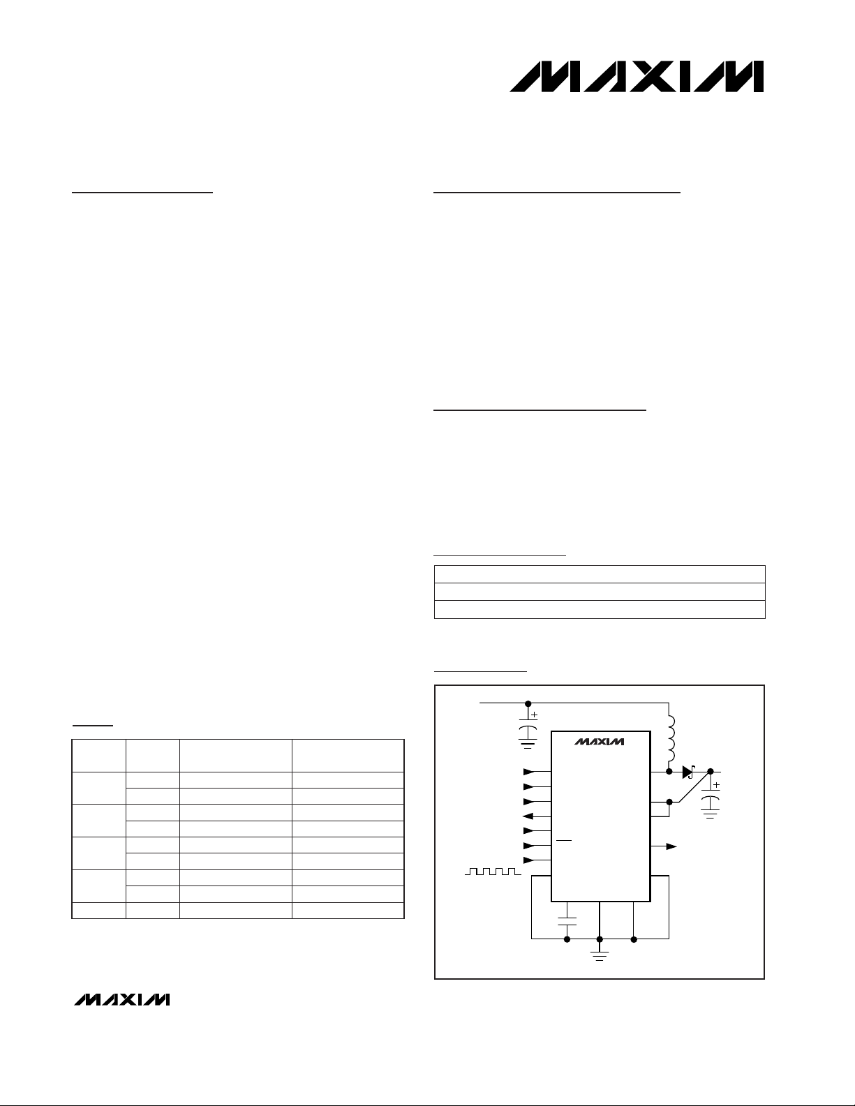
AIN1
AIN2
AINSEL
DATA
ON1
ON2
CLK/SEL
POKIN
LX
OUT
POUT
POK
FB
MAX848
MAX849
OUTPUT
A/D CHANNEL 1 IN
A/D CHANNEL 2 IN
A/D CHANNEL SELECT
A/D OUTPUT
ON/OFF CONTROL
SYNC INPUT
INPUT
0.8V TO 5.5V
VOLTAGE MONITOR
OUTPUT
REF
GND PGND
Typical Operating Circuit
19-1095; Rev 2; 12/97
PART
MAX848ESE
MAX849ESE
-40°C to +85°C
-40°C to +85°C
TEMP. RANGE PIN-PACKAGE
16 Narrow SO
16 Narrow SO
Ordering Information
Pin Configuration appears at end of data sheet.
Dual Mode is a trademark of Maxim Integrated Products.
Typical Output Selector Guide
V
IN
(V)
V
OU
T
(V)
MAX849 I
OUT
(mA)
MAX848 I
OUT
(mA)
0.9
3.3 100 70
5 70 40
1.2
3.3 300 110
5 200 70
2.4
3.3 750 200
5 500 130
2.7
3.3 800 250
5 600 150
3.6 5 1000 300
Page 2
mA
MAX848/MAX849
1-Cell to 3-Cell, High-Power,
Low-Noise, Step-Up DC-DC Converters
2 _______________________________________________________________________________________
ABSOLUTE MAXIMUM RATINGS
ELECTRICAL CHARACTERISTICS
(V
OUT
= 3.6V, GND = PGND = CLK/SEL = ON1 = ON2 = AINSEL = AIN1 = AIN2 = FB = POKIN, POUT = OUT, TA= 0°C to +85°C,
unless otherwise noted.)
Stresses beyond those listed under “Absolute Maximum Ratings” may cause permanent damage to the device. These are stress ratings only, and functional
operation of the device at these or any other conditions beyond those indicated in the operational sections of the specifications is not implied. Exposure to
absolute maximum rating conditions for extended periods may affect device reliability.
ON1, ON2, OUT, POUT to GND..................................-0.3V, +6V
PGND to GND ..........................................................-0.3V, +0.3V
LX to PGND ...............................................-0.3V, (V
POUT
+ 0.3V)
CLK/SEL, DATA, POKIN, REF,
AINSEL, AIN1, AIN2, FB, POK to GND .....-0.3V, (V
OUT
+ 0.3V)
Continuous Power Dissipation (T
A
= +70°C)
Narrow SO (derate 8.7mW/°C above +70°C) ................696mW
Operating Temperature Range
MAX848ESE/MAX849ESE .................................-40°C to +85°C
Junction Temperature......................................................+150°C
Storage Temperature.........................................-65°C to +160°C
Lead Temperature (soldering, 10sec).............................+300°C
110
300
70
VIN= 1.2V
200
200
750
V
OUT
= 5V
mA
1000
130
Output Current
VIN= 2.4V
500
I
REF
= 0mA
250
600
150
VIN= 2.7V
800
µA4 20
300
Operating Current in Shutdown
kHz40 300Frequency in Start-Up Mode
V0.9 1.1Minimum Start-Up Voltage (Note 5)
%-1.6
(Note 3)
Load Regulation (Note 4)
V1.23 1.25 1.27Reference Output Voltage
Current into OUT pin, V
ON2
= 3.6V
V0.7
V
OUT
= 1.5V
Minimum Operating Voltage (Note 1)
V2.1 2.4
VFB= 1.25V
Output Voltage Lockout Range
V2.7 5.5
Adjustable output, CLK/SEL = OUT
Output Voltage Adjust Range
nA200
-1µA < I
REF
< 50µA
FB Input Current
V1.215 1.240 1.265
2.5V < V
OUT
< 5V
FB Regulation Voltage
mV5 15REF Load Regulation
mV0.2 5
I
LOAD
< 1mA, TA> +25°C
REF Supply Rejection
VFB< 0.1V, CLK/SEL = OUT V3.17 3.34 3.40
CLK/SEL = OUT
Output Voltage (Note 2)
UNITSMIN TYP MAXPARAMETER
MAX848
MAX849
MAX848
MAX849
MAX848
MAX849
MAX848
MAX849
MAX848
MAX849
MAX848
MAX849
CONDITIONS
V
OUT
= 3.3V
V
OUT
= 5V
V
OUT
= 3.3V
MAX849, VIN= 3.6V
V
OUT
= 5V
V
OUT
= 3.3V
V
OUT
= 5V
MAX848, VIN= 3.3V
DC-DC CONVERTER
REFERENCE
Page 3
MAX848/MAX849
1-Cell to 3-Cell, High-Power,
Low-Noise, Step-Up DC-DC Converters
_______________________________________________________________________________________ 3
ELECTRICAL CHARACTERISTICS (continued)
(V
OUT
= 3.6V, GND = PGND = CLK/SEL = ON1 = ON2 = AINSEL = AIN1 = AIN2 = FB = POKIN, POUT = OUT, TA= 0°C to +85°C,
unless otherwise noted.)
Input Low Voltage
1.2V < V
OUT
< 5.5V, ON1 and ON2 (Note 8)
0.2V
OUT
Accuracy
V
Current into OUT pin, CLK/SEL = GND
V
OUT
= 2.7V, AINSEL and CLK/SEL
f
CLK
= 400kHz, 5ms conversion,
monotonic to 8 bits
±4 % FSR
0.2V
OUT
Internal Trip Level
µA
Rising V
OUT
, V
POKIN
< 0.1V 2.95 3.10 V
External Trip Level
Input High Voltage
Rising V
POKIN
1.225 1.275
µA1 2f
CLK
= 400kHz, V
AIN1
= V
AIN2
= 2.5VAIN1, AIN2 Input Current
V0 2.5AINSEL = OUTAIN2 Input Voltage Range
V0.625 1.875AINSEL = GNDAIN1 Input Voltage Range
VV
OUT
- 0.4
V
Data Output Voltage High
V0.4
I
SOURCE
= 1mA
Data Output Voltage Low I
SINK
= 1mA
POK Low Voltage
1.2V < V
OUT
< 5.5V, ON1 and ON2 (Note 8)
I
SINK
= 1mA, V
OUT
= 3.6V or
I
SINK
= 20µA, V
OUT
= 1V
0.4 V
POK High Leakage Current
0.8V
OUT
V
OUT
= V
POK
= 5.5V 0.01 1 µA
POKIN Leakage Current
V
V
POKIN
= 1.5V 50 nA
35 90
V
OUT
= 5.5V, AINSEL and CLK/SEL 0.8V
OUT
Operating Current in Low-Power
Mode (Note 6)
Logic Input Current
ON1, ON2, AINSEL and CLK/SEL
1 µA
Internal Oscillator Frequency CLK/SEL = OUT 260 300 340 kHz
Oscillator Maximum Duty Cycle 80 85 90 %
External Clock Frequency Range 200 400 kHz
CLK/SEL Pulse Width Not tested 200 ns
CLK/SEL Rise/Fall Time Not tested 100 ns
Current into OUT pin, CLK/SEL = OUT,
does not include switching losses
µA
150 300
UNITS
MIN TYP MAX
CONDITIONSPARAMETER
Operating Current in Low-Noise
Mode (Note 6)
VLX= 0V, V
ON2
= V
OUT
= 5.5V µA0.1 20POUT Leakage Current
VLX= V
ON2
= V
OUT
= 5.5V µA0.1 20LX Leakage Current
N-channel
0.3 0.6
CLK/SEL = GND
0.13 0.25
CLK/SEL = OUT
P-channel
Ω
0.25 0.5
Switch On-Resistance
CLK/SEL = OUT
600 800 1000MAX848
CLK/SEL = OUT
1100 1350 1600MAX849
120 200 300MAX848
V
CLK/SEL
= 0V (Note 7)
mA
250 400 550
N-Channel Current Limit
MAX849
DC-DC SWITCHES
ADC
POWER-GOOD
LOGIC AND CONTROL INPUTS
Page 4
MAX848/MAX849
1-Cell to 3-Cell, High-Power,
Low-Noise, Step-Up DC-DC Converters
4 _______________________________________________________________________________________
ELECTRICAL CHARACTERISTICS
(V
OUT
= 3.6V, GND = PGND = CLK/SEL = ON1 = ON2 = AINSEL = AIN1 = AIN2 = FB = POKIN, POUT = OUT, TA= -40°C to +85°C,
unless otherwise noted.) (Note 9)
Note 1: Minimum operating voltage. Because the MAX848/MAX849 are bootstrapped to the output, it will operate down to a 0.7V input.
Note 2: In low-power mode (CLK/SEL = GND), the output voltage regulates 1% higher than in low-noise mode (CLK/SEL = OUT or
synchronized).
Note 3: The part is in start-up mode until it reaches this voltage level. Do not apply full-load current.
Note 4: Load regulation is measured from no load to full load, where full load is determined by the N-channel switch current limit.
Note 5: Start-up is tested with Figure 2’s circuit. Output current is measured when the input and output voltages are applied.
Note 6: Supply current from the 3.34V output is measured between the 3.34V output and the OUT pin. This current correlates directly
with actual battery supply current, but is reduced in value according to the step-up ratio and efficiency. V
OUT
= 3.6V to keep
the internal switch open when measuring the current into the device.
Note 7: When V
CLK/SEL
= 0V, the inductor is forced into constant-peak-current, discontinuous operation. This is guaranteed by
testing in Figure 2’s circuit.
Note 8: ON1 and ON2 inputs have approximately 0.15V
OUT
hysteresis.
Note 9: Specifications to -40°C are guaranteed by design, not production tested.
%80 90Oscillator Maximum Duty Cycle
kHz260 340CLK/SEL = OUTInternal Oscillator Frequency
V1.225 1.275Rising V
POKIN
External Trip Level
V2.95 3.10Rising V
OUT
, V
POKIN
< 0.1VInternal Trip Level
% FSR±4f
CLK
= 400kHz, 5ms conversionAccuracy
250 550MAX849
CLK/SEL = GND (Note 7)
N-Channel Current Limit
120 300MAX848
PARAMETER CONDITIONS
MIN TYP MAX
UNITS
1100 1800MAX849
CLK/SEL = OUT
mA
600 1100MAX848
0.5CLK/SEL = OUTP-channel
Switch On-Resistance 0.25CLK/SEL = OUT
N-channel
I
REF
= 0mAReference Output Voltage 1.225 1.275 V
Ω
Output Voltage (Note 3)
VFB< 0.1V, CLK/SEL = OUT,
includes load-regulation error
3.13 3.47 V
FB Regulation Voltage Adjustable output, CLK/SEL = OUT 1.21 1.27 V
Output Voltage Lockout Range (Note 3) 2.05 2.45 V
0.6CLK/SEL = GND
µA300
CLK/SEL = OUT, does not include
switching losses
OUT Supply Current in Low-Noise
Mode (Note 6)
µA90CLK/SEL = GND
OUT Supply Current in Low-Power
Mode (Note 6)
OUT Supply Current in Shutdown V
ON2
= 3.6V 20 µA
REFERENCE
DC-DC CONVERTER
DC-DC SWITCHES
ADC
POWER-GOOD
LOGIC CONTROL INPUTS
Page 5
MAX848/MAX849
1-Cell to 3-Cell, High-Power,
Low-Noise, Step-Up DC-DC Converters
_______________________________________________________________________________________
5
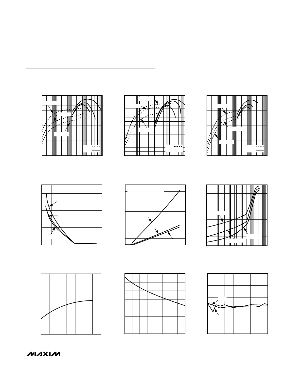
Typical Operating Characteristics
(TA = +25°C, unless otherwise noted.)
100
90
40
0.1 1 10 100 1000
MAX849
EFFICIENCY vs. LOAD CURRENT
(V
OUT
= 3.3V)
50
MAX848/9 TOC-01
LOAD CURRENT (mA)
EFFICIENCY (%)
60
70
80
VIN = 2.4V
PFM
PWM
VIN = 0.9V
VIN = 1.2V
100
90
40
30
0.1 1 10 100 1000
MAX849
EFFICIENCY vs. LOAD CURRENT
(V
OUT
= 5V)
50
MAX848/9 TOC-02
LOAD CURRENT (mA)
EFFICIENCY (%)
60
70
80
VIN = 1.2V
VIN = 2.4V
VIN = 3.6V
PFM
PWM
70
60
0.1 1 10 100 1000
MAX848
EFFICIENCY vs. LOAD CURRENT
(V
OUT
= 3.3V)
80
MAX848/9 TOC-03
LOAD CURRENT (mA)
EFFICIENCY (%)
90
100
VIN = 2.4V
VIN = 1.2V
VIN = 0.9V
PFM
PWM
14
0
0 2 31 4 6
NO-LOAD BATTERY CURRENT
vs. INPUT VOLTAGE
4
12
MAX848/9 TOC-04
INPUT VOLTAGE (V)
INPUT CURRENT (mA)
5
8
2
10
6
TA = +85°C
TA = +25°C
TA = -40°C
1.252
1.248
-40 0
-20
20 60 10080
REFERENCE VOLTAGE
vs. TEMPERATURE
1.249
1.251
MAX848/9 TOC-07
TEMPERATURE (°C)
REFERENCE VOLTAGE (V)
40
1.250
18
14
0
0 21 3 65
SHUTDOWN CURRENT
vs. INPUT VOLTAGE
4
16
12
MAX848/9 TOC-05
SHUTDOWN CURRENT (µA)
4
8
2
10
6
TA = +85°C
TA = +25°C
TA = -40°C
INCLUDES ALL EXTERNAL
COMPONENT LEAKAGES.
CAPACITOR LEAKAGE
DOMINATES AT
T
A
= +85°C
INPUT VOLTAGE (V)
2.0
1.8
1.6
0.6
0.01 0.1 1 10 100 1000
START-UP VOLTAGE vs. LOAD CURRENT
(V
OUT
= 3.3V, PWM MODE)
0.8
MAX848/9 TOC-06
LOAD CURRENT (mA)
START-UP VOLTAGE (V)
1.0
1.2
1.4
TA = +85°C
TA = +25°C
TA = -40°C
1.252
1.238
0 2010 30 50 60 70 80
REFERENCE VOLTAGE
vs. REFERENCE CURRENT
1.242
1.250
MAX848/9 TOC-08
REFERENCE CURRENT (µA)
REFERENCE VOLTAGE (V)
40
1.246
1.240
1.248
1.244
0.25
-0.25
0.1875 0.68750.4375 0.9375
ADC LINEARITY ERROR
vs. FULL-SCALE INPUT VOLTAGE
0.15
MAX848/9 TOC-09
FULL-SCALE INPUT VOLTAGE (V)
LINEARITY ERROR (%FS)
-0.15
0.05
-0.05
AIN1
AIN2
Page 6

MAX848/MAX849
1-Cell to 3-Cell, High-Power,
Low-Noise, Step-Up DC-DC Converters
6 _______________________________________________________________________________________
Typical Operating Characteristics (continued)
(TA = +25°C, unless otherwise noted.)
VIN = 1.1V, I
OUT
= 200mA, V
OUT
= 3.3V
A = LX VOLTAGE, 2V/div
B = INDUCTOR CURRENT, 0.5A/div
C = V
OUT
RIPPLE, 50mV/div, AC COUPLED
HEAVY-LOAD SWITCHING WAVEFORMS
(V
OUT
= 3.3V)
A
B
C
0A
0V
V
OUT
1µs/div
MAX848/9 TOC-10
VIN = 1.1V, V
OUT
= 3.3V
A = LOAD CURRENT, 0mA TO 200mA, 0.2A/div
B = V
OUT
RIPPLE, 50mV/div, AC COUPLED
LOAD-TRANSIENT RESPONSE
A
B
0A
200mA
2ms/div
MAX848/9 TOC-12
I
OUT
= 0mA, V
OUT
= 3.3V
A = V
IN
, 1.1V TO 2.1V, 1V/div
B = V
OUT
RIPPLE, 50mV/div, AC COUPLED
LINE-TRANSIENT RESPONSE
A
B
0V
5ms/div
MAX848/9 TOC-11
A = V
ON1
, 2V/div
B = V
OUT
, 1V/div
C = INPUT CURRENT, 0.2A/div
POWER-ON DELAY
(PFM MODE)
A
B
C
0mA
3.3V
5ms/div
MAX848/9 TOC-13
Page 7

MAX848/MAX849
1-Cell to 3-Cell, High-Power,
Low-Noise, Step-Up DC-DC Converters
_______________________________________________________________________________________ 7
Typical Operating Characteristics (continued)
(TA = +25°C, unless otherwise noted.)
VIN = 3.6V, V
OUT
= 5V, C
OUT
= 440µF
A = V
OUT
RIPPLE, 200mV/div, AC COUPLED
B = LOAD CURRENT, 100mA TO 1A, 0.5A/div,
PULSE WIDTH = 577µs
MAX849
GSM LOAD-TRANSIENT RESPONSE
A
5V
0A
B
1ms/div
MAX848/9 TOC-14
VIN = 1.2V, V
OUT
= 3.3V, C
OUT
= 440µF
A = V
OUT
RIPPLE, 200mV/div, AC COUPLED
B = LOAD CURRENT, 50mA TO 400mA, 0.2A/div,
PULSE WIDTH = 416µs
MAX849
DECT LOAD-TRANSIENT RESPONSE
A
B
3.3V
0A
2ms/div
MAX848/9 TOC-15
2.7
0.1k 1k 10k 100k 1M
MAX849 NOISE SPECTRUM
(V
OUT
= 3.3V, VIN = 1.2V, R
LOAD
= 50Ω)
0
MAX848/9 TOC-16
FREQUENCY (Hz)
NOISE (mV
RMS
)
380
280
-40 100
MAX849 INTERNAL OSCILLATOR
FREQUENCY vs. TEMPERATURE
360
MAX848/9 TOC-17
TEMPERATURE (°C)
INTERNAL OSC. FREQUENCY (kHz)
20
320
300
-20 0 60
340
40
80
V
OUT
= 5V
V
OUT
= 3.3V
1.2
2.5 3.53.0 4.0 5.55.0
MAX849 PEAK INDUCTOR CURRENT
vs. OUTPUT VOLTAGE
1.4
1.8
2.0
MAX848/9 TOC-18
OUTPUT VOLTAGE (V)
PEAK INDUCTOR CURRENT (A)
4.5
1.6
1.3
1.7
1.5
Page 8

MAX848/MAX849
1-Cell to 3-Cell, High-Power,
Low-Noise, Step-Up DC-DC Converters
8 _______________________________________________________________________________________
Pin Description
ADC’s Input Channel Selector. Pull low to select AIN1 and drive high to select AIN2.AINSEL9
ADC’s Serial Output. Pulsed output, RZ format. Full scale is f
OSC
/2 (
f
CLK
/2
in external sync mode). The
DATA output is low when V
CLK/SEL
= 0V (PFM mode).
DATA10
External Clock Input/Regulator’s Switching Mode Selector.
CLK/SEL = low: low-power, low-quiescent PFM mode. Delivers 100mW of output power.
CLK/SEL = high: low-noise, high-power PWM mode, switching at a constant frequency (300kHz).
CLK/SEL = driven with external clock: low-noise, high-power, synchronized PWM mode. The internal
oscillator is synchronized to the external clock (200kHz ~ 400kHz). Turning the DC-DC converter on with
V
CLK/SEL
= 0V also serves as a soft-start function, since the peak inductor current is limited to 30% of the
nominal value.
CLK/SEL11
Source of the Internal N-Channel Power MOSFET. Connect to high-current ground path.PGND12
Drain of the Internal N-Channel Power MOSFET and P-Channel Synchronous RectifierLX13
Output Sense Input. The IC is powered from OUT. Bypass to GND with a 0.1µF ceramic capacitor. Connect
OUT to POUT through a 10Ω series resistor.
OUT5
Power-Good Comparator Input. Connect to GND for fixed threshold (V
OUT
x 0.9). To adjust the threshold,
connect to a resistor divider from OUT to GND.
POKIN6
Dual Mode DC-DC Converter Feedback Input. Connect to GND for fixed 3.3V output voltage. Connect to
a resistor divider from OUT to GND to adjust the output voltage. Minimize noise coupling from switching
signals to FB.
FB7
Power-Good Output. This open-drain output is pulled low when the output voltage (V
OUT
) drops below
the internally set threshold (fixed threshold), or when the voltage at POKIN drops below V
REF
(adjustable
threshold).
POK8
Ground. Use for low-current ground paths. Connect to PGND with a short trace.GND4
Reference Output. Bypass with a 0.22µF capacitor to GND.REF3
PIN
ADC’s Channel 2 Input. Analog input voltage range is 0V to 2.5V.AIN22
ADC’s Channel 1 Input. Analog input voltage range is 0.625V to 1.875V.AIN1
1
FUNCTIONNAME
14 POUT
Source of the Internal P-Channel Synchronous Rectifier MOSFET. Connect an external Schottky diode from
LX to POUT. Bypass to PGND with a 0.1µF ceramic capacitor as close to the IC as possible.
15
ON2 OFF Control Input. When ON1 = 0 and ON2 = 1, the IC is off.
16 ON1
ON Control Input. When ON1 = 1 or ON2 = 0, the IC is on.
Page 9

MAX848/MAX849
1-Cell to 3-Cell, High-Power,
Low-Noise, Step-Up DC-DC Converters
_______________________________________________________________________________________ 9
_______________Detailed Description
The MAX848/MAX849 combine a switching regulator,
N-channel power MOSFET, P-channel synchronous
rectifier, precision reference voltage, power-good indicator, and battery voltage monitor, all in a single monolithic device. The MAX848/MAX849 are powered
directly from the output. The output voltage is factory
preset to 3.3V or adjustable from 2.7V to 5V with external resistors (Dual Mode™ operation). These devices
start from a low 1V input voltage and remain operational down to 0.7V. The MAX848/MAX849 operate with
either one to three NiCd/NiMH cells or one Li-Ion cell.
At power-up, an internal low-voltage oscillator drives
the N-channel power switch, and the output voltage
slowly builds up. The oscillator has a 25% nominal duty
cycle to prevent current build-up in the inductor. An
output voltage in excess of the nominal 2.25V lockout
voltage activates the error comparator and internal timing circuitry. The device resumes operation in either
pulse-frequency-modulation (PFM) low-power mode or
pulse-width-modulation (PWM) low-noise mode, selected by the logic control, CLK/SEL. Figure 2 shows the
standard application circuit for the MAX849 configured
in the high-power PWM mode.
On/Off Control
The MAX848/MAX849 are turned on or off by logic
input pins ON1 and ON2 (Table 1). When ON1 = 1 or
ON2 = 0, the part is on. When ON1 = 0 and ON2 = 1,
the part is off. Both inputs have logic trip points near
0.5 x V
OUT
with 0.15 x V
OUT
hysteresis.
Operating Modes
The MAX848/MAX849 operate in either PFM, PWM, or
PWM synchronized to an externally applied clock signal. Table 2 lists each operating mode.
ON
REF
1.25V
RDY
EN
START-UP
OSCILLATOR
Q
OUT
ON1
ON2
REF
GND
CLK/SEL
FB
POKIN
AINSEL
AIN1
AIN2
EN
ADC
FEEDBACK
EN
300kHz
OSCILLATOR
2.25V
FEEDBACK
AND
POWER-GOOD
SELECT
PFM/PWM
PCH
0.25Ω
NCH
0.13Ω
POUT
LX
PGND
POK
DATA
MAX848/MAX849
N
Q
Q
D
EN
OSC
MODE
PFM/PWM
CONTROLLER
Figure 1. Functional Diagram
ON1
OONN22
MAX848/MAX849
0 0 On
0 1 Off
1 0 On
1 1 On
Table 1. On/Off Logic Control
Page 10

MAX848/MAX849
1-Cell to 3-Cell, High-Power,
Low-Noise, Step-Up DC-DC Converters
10 ______________________________________________________________________________________
Low-Power PFM Mode
When CLK/SEL is pulled low, the MAX848/MAX849 operate in low-power, low-supply-current PFM mode. Pulsefrequency modulation provides the highest efficiency at
light loads. The P-channel rectifier is turned off to reduce
gate-charge losses, and the regulator operates in discontinuous mode. The N-channel power MOSFET is kept
on until the inductor current ramps to 30% of the current
limit. The inductor energy is delivered to the output
capacitor when the switch turns off. A new cycle is inhibited until the inductor current crosses zero. Zero current
detection is accomplished by sensing the LX voltage
crossing the output voltage. Figure 3 shows the block
diagram for the PFM controller.
Low-Noise PWM Mode
When CLK/SEL is pulled high, the MAX848/MAX849
operate in high-power, low-noise, current-mode PWM,
switching at the 300kHz nominal internal oscillator frequency. The internal rectifier is active in this mode,
and the regulator operates in continuous mode. The
N-channel power MOSFET turns on until either the output
voltage is in regulation or the inductor current limit is
reached (0.8A for the MAX848 and 1.4A for the
MAX849). The switch turns off for the remainder of the
cycle and the inductor energy is delivered to the output
capacitor. A new cycle is initiated on the next oscillator
cycle. In low-noise applications, the fundamental and the
harmonics generated by the fixed switching frequency
can easily be filtered. Figure 4 shows the block diagram
for the PWM controller.
The MAX848/MAX849 enter synchronized current-mode
PWM when a clock signal (200kHz < f
CLK
< 400kHz) is
applied to CLK/SEL. The internal synchronous rectifier
is active and the switching frequency is synchronized
to the externally applied clock signal. For wireless
applications, this ensures that the harmonics of the
switching frequencies are predictable and can be kept
outside the IF band(s). High-frequency operation permits low-magnitude output ripple voltage.
The MAX848/MAX849 are capable of providing a stable
output even with a rapidly pulsing load (GSM, DECT),
such as from a transmitter power amplifier in digital cordless phones (see
Typical Operating Characteristics
).
In PWM mode, the use of the synchronous rectifier
ensures constant-frequency operation, regardless of
the load current.
Setting the Output Voltage Externally
The MAX848/MAX849 feature Dual Mode operation.
The output voltage is preset to 3.3V (FB = 0V), or it can
be adjusted from 2.7V to 5.5V with external resistors
R1, R2, and R3, as shown in Figure 5. To set the output
voltage externally, select resistor R3 in the 10kΩ to
100kΩ range. The values for R1 and R2 are given by:
R2 = R3(V
OUT
/ V
TRIP
- 1)
R1 = (R3 + R2)(V
TRIP
/ V
REF
- 1)
MAX849
C5
0.1µF
V
IN
= 1.1V
C2
0.1µF
C3
0.22µF
C1
22µF
OUT
GND
POK
ON1
ON2
CLK/SEL
REF
PGND
FB
POKIN
LX
POUT
C4
2 x 100µF
L1
10µH
D1
MBR0520L
3.3V @
200mA
R3
100k
10Ω
*
HEAVY LINES INDICATE
HIGH-CURRENT PATH.
*
Figure 2. 3.3V Preset Output
Table 2. Selecting Operating Mode
CLK/SEL MODE
0 PFM
1 PWM
External clock
(200kHz ~ 400kHz)
Synchronized PWM
Figure 3. Controller Block Diagram in PFM Mode
FEEDBACK
REF
PFM-MODE
CURRENT-
LIMIT LEVEL
S
R
Q
R
DQ
CURRENT
SENSE
LOGIC HIGH
POUT
LX
N
PGND
Page 11

MAX848/MAX849
1-Cell to 3-Cell, High-Power,
Low-Noise, Step-Up DC-DC Converters
______________________________________________________________________________________ 11
where V
REF
= 1.25V, V
OUT
is the desired output volt-
age, and V
TRIP
is the desired trip level for the power-
good comparator.
Power-OK
The MAX848/MAX849 feature a power-good comparator. This comparator’s open-drain output, POK, is
pulled low when the output voltage falls below the nominal internal threshold level of 3V with POKIN = 0V. To
set the power-good trip level externally, refer to the
Setting the Output Voltage Externally
section.
Analog-to-Digital Converter (ADC)
The MAX848/MAX849 have an internal, two-channel, serial ADC. The ADC converts an analog input voltage into a
digital stream available at the DATA pin. The converter
skips clock pulses in proportion to the input voltage.
Output format is a return-to-zero bit stream with a bit
duration of 1/f
CLK
. At zero-scale input voltage, all pulses
are skipped and DATA remains low; with a positive fullscale input voltage, no pulses are skipped; and at midscale, every other pulse is skipped. The ADC’s clock is
one-half of the externally applied clock signal or one-half
of the internal 300kHz clock available at LX. In PFM
mode, the converter is not active and DATA is driven low.
Channel 1, AIN1, has an input voltage range of 0.625V
to 1.875V and is selected when AINSEL is low. Channel
2, AIN2, accepts inputs in the 0V to 2.5V range and is
selected when AINSEL is pulled high (Figure 6).
The ADC is a switched-capacitor type; therefore, an
anti-aliasing filter might be required at the inputs. Insert
a 1kΩ series resistor and a 0.01µF filter capacitor in
noisy environments.
Timer Function Implementation
Implement the necessary counter functions either with
discrete hardware or with microcontroller (µC) implementations. The output resolution depends on how
many of the ADC clock pulses are counted, as shown
in Figure 7.
Hardware Implementation
A complete hardware solution can be implemented
using either two counters or an ASIC. Resolution
depends on how many pulses are counted. The main
advantage of the discrete hardware implementation is
that accuracy is not affected by interrupt latency associated with the µC solution.
RSQ
OSC
PWM-MODE
CURRENT-
LIMIT LEVEL
REF
FEEDBACK
POUT
LX
PGND
N
P
Figure 4. Controller Block Diagram in PWM Mode
MAX848
MAX849
OUT
POKIN
FB
POK
GND
OUTPUT
R1
R2
R3
Figure 5. Adjustable Output Voltage and Power-Good Trip Level
C/2
C/2
C
REF
C
D Q
÷2
2 x REF
AIN2
OSC
AINSEL
AIN1
DATA
Figure 6. A/D Converter Block Diagram
Page 12

MAX848/MAX849
1-Cell to 3-Cell, High-Power,
Low-Noise, Step-Up DC-DC Converters
12 ______________________________________________________________________________________
When using two counters of the same length, as shown
in Figure 8, one counter (A) just counts the A/D clock
pulses (f
OSC
/2), and the other counter (B) counts DATA
output pulses. When counter A overflows (for example,
after 256 clock cycles for an 8-bit counter), counter B is
disabled. The controller reads the counter B output
data and calculates the analog voltage present at the
ADC’s input.
All µC Implementation
This implementation uses a µC timer and a counter.
The timer and the counter are reset at the same time.
The counter counts data-output pulses applied at its
input. When the timer times out, an interrupt is asserted. The µC then reads the state of the counter register.
The interrupt-handling overhead can cause the counter
to count more pulses than desired. Accuracy depends
on how long the µC needs to read the counter. No
errors will occur if the counter is disabled within one
clock period. Interrupt latency reduces accuracy. The
main advantage of this implementation is that no external hardware is required.
__________________Design Procedure
Inductor Selection
The MAX848/MAX849’s high switching frequency allows
the use of a small inductor. Use a 10µH inductor for the
MAX849 and a 22µH inductor for the MAX848. Inductors
with a ferrite core or equivalent are recommended; powder iron cores are not recommended for use with high
switching frequencies. Make sure the inductor’s saturation rating (the current at which the core begins to saturate and inductance starts to fall) exceeds the internal
current limit: 0.8A for the MAX848 and 1.4A for the
MAX849. However, it is generally acceptable to bias the
inductor into saturation by approximately 20% (the point
where the inductance is 20% below the nominal value).
For highest efficiency, use a coil with low DC resistance,
preferably under 100mΩ. To minimize radiated noise,
use a toroid, pot core, or shielded inductor. See Table 5
for a list of suggested inductor suppliers.
Diode Selection
The MAX848/MAX849’s high switching frequency
demands a high-speed rectifier. Schottky diodes, such
as the 1N5817 or MBR0520L, are recommended. Make
sure the diode’s current rating exceeds the maximum
load current and that its breakdown voltage exceeds
V
OUT
.
The Schottky rectifier diode carries load currents only in
the PFM operating mode, since the P-channel synchronous rectifier is disabled. Therefore, the current rating
need not be high (0.5A is sufficient). In PFM mode, the
voltage drop across the rectifier diode causes efficiency loss. However, when operating in PWM mode, the
internal P-channel synchronous rectifier is active and
efficiency loss due to the rectifier diode is minimized.
For high-temperature applications, Schottky diodes
may be inadequate due to their high leakage currents;
use high-speed silicon diodes such as the MUR105 or
EC11FS1. At heavy loads and high temperatures, the
benefits of a Schottky diode’s low forward voltage may
outweigh the disadvantage of high leakage current.
See Table 4 for a list of suggested diode suppliers.
f
OSC
/2
DATA
GIVES YOU 2-BIT RESOLUTION
COUNTING FOUR PULSES
Figure 7. Bit Stream at 1/2 Full Scale
EN
CLR
CLK RC8-BIT COUNTER
CLR
CLK
EN8-BIT COUNTER
LATCH
÷2
V
CC
CLOCK/SEL
OR LX
CLEAR
CARRY OUTPUT
DATA OUTPUT
A
B
Figure 8. Discrete Hardware Solution for Counting A/D Output
Data Pulses
Page 13

MAX848/MAX849
1-Cell to 3-Cell, High-Power,
Low-Noise, Step-Up DC-DC Converters
______________________________________________________________________________________ 13
Capacitor Selection
Input Bypass Capacitors
A 22µF, low-ESR input capacitor will reduce peak currents and reflected noise due to inductor current ripple.
Smaller ceramic capacitors may also be used for light
loads or in applications that can tolerate higher input
ripple.
Output Filter Capacitors
Two 100µF (single 100µF for the MAX848), 10V, lowESR, output filter capacitors typically exhibit 30mV ripple when stepping up from 1.2V to 3.3V at 200mA
(100mA for the MAX848). Bypass the MAX848/MAX849
supply input, OUT, with a 0.1µF ceramic capacitor
to GND. Also bypass POUT to PGND with a 0.1µF
ceramic capacitor.
The filter capacitors’ equivalent series resistance (ESR)
affects efficiency and output ripple. The output voltage
ripple is the product of the peak inductor current and
the output capacitor’s ESR. Low-ESR, surface-mount
tantalum capacitors are currently available from
Sprague (595D series) and AVX (TPS series). Sanyo
OS-CON organic-semiconductor, through-hole capacitors also exhibit very low ESR, and are especially useful
for operation at cold temperatures. See Table 5 for a list
of suggested capacitor suppliers.
Applications Information
Using a Momentary On/Off Switch
A momentary pushbutton switch can be used to turn
the MAX848/MAX849 on and off.
As shown in Figure 9, ON1 is pulled low and ON2 is
pulled high when the part is off. When the momentary
switch is pressed, ON2 is pulled low and the regulator
turns on. The switch should be on long enough for the
µC to exit reset. The controller issues a logic high to
ON1, which guarantees that the part will stay on,
regardless of the switch state.
To turn off the regulator, the switch is pressed and held.
The controller reads the switch status and pulls ON1
low. The switch is released and ON2 is pulled high.
Power Amplifier (PA) and Radio Supply
in a Typical Phone Application
The MAX849 is an ideal power supply for the power
amplifier (PA) and the radio used in digital cordless
and PCS phones (Figure 10). The PA is directly powered by the MAX849 for maximum output swing. Postlinear regulators power the controller and the radio. In
addition, they reduce switching noise and ripple. Table
3 lists the output power available when operating with
one or more NiCd/NiMH cells or one Li-Ion cell.
MAX848
MAX849
ON1
ON2 V
DD
I/O
I/O
OUT
µC
1MΩ
1MΩ
Figure 9. Momentary Pushbutton On/Off Switch
MAX848
MAX849
µC
MAX8865/MAX8866 DUALS
MAX8863/MAX8864 SINGLES
RADIO
PA
Figure 10. Typical Phone Application
NUMBER OF CELLS
INPUT VOLTAGE
(V)
OUTPUT VOLTAGE:
PA POWER SUPPLY
(V)
OUTPUT POWER
(W)
1 NiCd/NiMH 1.2 3.3 0.9
2 NiCd/NiMH 2.4 3.3 2.4
2 NiCd/NiMH 2.4 5.0 2.6
3 NiCd/NiMH or 1 Li-Ion 3.6 5.0 4.3
Table 3. Available Output Power
Page 14

MAX848/MAX849
1-Cell to 3-Cell, High-Power,
Low-Noise, Step-Up DC-DC Converters
14 ______________________________________________________________________________________
Power-On Reset Delay
Adding a timing capacitor from POK to GND generates
a power-on reset delay. The reset time constant is
determined by the pull-up resistor and timing capacitor
(Figure 11). When power is turned on, POK is low and
the capacitor is shorted. When the output voltage
reaches regulation, POK goes high and the capacitor
slowly charges to the output voltage.
The timing resistor value depends on the controller’s
RESET input leakage current. The voltage drop across
the timing resistor should not exceed the difference
between the output voltage and the µC reset threshold
voltage. This resistor should be large enough to minimize the shutdown current.
µC-Controlled Shutdown
The MAX848/MAX849 turn on when ON1 = 1 or ON2 = 0.
The µC monitors the battery voltage and turns off the
device (forces ON1 low and ON2 high) when the battery is weak.
Layout Considerations
Due to high inductor current levels and fast switching
waveforms, which radiate noise, proper PC board layout is essential. Protect sensitive analog grounds by
using a star ground configuration. Minimize ground
noise by connecting PGND, the input bypass capacitor
ground lead, and the output filter capacitor ground lead
to a single point (star ground configuration). Also, minimize lead lengths to reduce stray capacitance and
trace resistance.
If an external resistor divider is used to set the output
voltage (Figure 5), the trace from FB to the resistors
must be extremely short and must be shielded from
switching signals, such as CLK, DATA, or LX.
MAX848
MAX849
OUT
POK
V
CC
RESET
µC
R
C
Figure 11. Power-On Reset Delay
Table 4. Component Selection Guide
PRODUCTION INDUCTORS CAPACITORS DIODES
Surface Mount
Sumida CDR63B, CD73, CDR73B, CD74B series
Coilcraft DO1608, DO3308, DT3316 series
Matsuo 267 series
Sprague 595D series
AVX TPS series
Motorola MBR0520L
Through Hole Sumida RCH654 series
Sanyo OS-CON series
Nichicon PL series
Motorola 1N5817
Table 5. Component Suppliers
SUPPLIER PHONE FAX
AVX
USA: 803-946-0690
800-282-4975
803-626-3123
Coilcraft USA: 847-639-6400 847-639-1469
Matsuo USA: 714-969-2491 714-960-6492
Motorola USA: 602-303-5454 602-994-6430
Sanyo
USA: 619-661-6835
Japan: 81-7-2070-6306
619-661-1055
81-7-2070-1174
Sumida
USA: 847-956-0666
Japan: 81-3-3607-5111
847-956-0702
81-3-3607-5144
Chip Information
TRANSISTOR COUNT: 2059
Page 15

MAX848/MAX849
1-Cell to 3-Cell, High-Power,
Low-Noise, Step-Up DC-DC Converters
______________________________________________________________________________________ 15
16
15
14
13
12
11
10
9
1
2
3
4
5
6
7
8
ON1
ON2
POUT
LX
PGND
CLK/SEL
DATA
AINSEL
AIN1
AIN2
REF
GND
OUT
POKIN
FB
POK
TOP VIEW
MAX848
MAX849
Narrow SO
Pin Configuration
Package Information
SOICN.EPS
Page 16

MAX848/MAX849
1-Cell to 3-Cell, High-Power,
Low-Noise, Step-Up DC-DC Converters
Maxim cannot assume responsibility for use of any circuitry other than circuitry entirely embodied in a Maxim product. No circuit patent licenses are
implied. Maxim reserves the right to change the circuitry and specifications without notice at any time.
16
____________________Maxim Integrated Products, 120 San Gabriel Drive, Sunnyvale, CA 94086 408-737-7600
© 1998 Maxim Integrated Products Printed USA is a registered trademark of Maxim Integrated Products.
NOTES
 Loading...